Tunneling magnetoresistance devices based on topological insulators: Ferromagnet/insulator/topological-insulator junctions employing Bi2Se3
Abstract
We theoretically investigate tunneling magnetoresistance (TMR) devices, which are probing the spin-momentum coupled nature of surface states of the three-dimensional topological insulator Bi2Se3. Theoretical calculations are performed based on a realistic tight-binding model for Bi2Se3. We study both three dimensional devices, which exploit the surface states of Bi2Se3, as well as two-dimensional devices, which exploit the edge states of thin Bi2Se3 strips. We demonstrate that the material properties of Bi2Se3 allow a TMR ratio at room temperature of the order of 1000 %. Analytical formulas are derived that allow a quick estimate of the achievable TMR ratio in these devices. The devices can be used to measure the spin polarization of the topological surface states as an alternative to spin-ARPES. Unlike TMR devices based on magnetic tunnel junctions the present devices avoid the use of a second ferromagnetic electrode whose magnetization needs to be pinned.
I Introduction
Topological insulators (TI) are materials which possess an insulating gap in the bulk but conducting states at the surface. These surface states are protected by the topological properties of the material and are robust against time-reversal-symmetric perturbations like non-magnetic impurities, for example. After first being predicted theoretically, Bernevig ; Fu subsequently several materials have been confirmed to be topological insulators experimentally. Koenig ; Hsieh1 ; Chen ; Xia ; Hsieh2 ; Kuroda ; Ando Due to spin-orbit coupling the momentum of the surface states is locked with the spin of the electrons, which means that electrons with opposite spin propagate into opposite direction Ando ; Hsieh ; Bruene ; Pan:PRL106 . The robustness of the surface states against backscattering promises long spin diffusion lengths. These features make topological insulators particularly interesting for applications in spintronics Tanaka ; Mondal ; Linder ; Garate ; Yokoyama ; BlackSchaffer ; Krueckl ; Kong ; Salehi ; Vali ; PGGD ; Taguchi . In addition, spin-dependent tunneling into the surface states opens a way to investigate their properties such as spin-polarization.
In the present work we theoretically study different arrangements to realize a tunneling magnetoresistance (TMR) device using a ferromagnet coupled via a tunnel barrier to a topological insulator. In contrast to conventional TMR junctions such a device does not need a second ferromagnetic layer, because the spin locking in the topological insulator already provides an intrinsic magnetic reference. Additionally, the device can be used to probe the spin-locked surface states in the TI. We will show that the material properties of the topological insulator determine the maximum TMR ratio that can be achieved. Specifically, we will present calculations for the three-dimensional topological insulator Bi2Se3, which has been studied well in the past both theoretically and experimentally Zhang:NPhys09 ; Xia ; Liu:PRB10 ; Li:NPhys10 ; Shan . This material is particularly interesting due to its comparatively large band gap of about 0.3 eV. As we will see, this allows to achieve large TMR ratios already at room temperature.
II Model
For our calculations we are using a realistic tight-binding model for Bi2Se3 that has been derived from bandstructure calculations by Liu et al Liu:PRB10 based on theory. The Hamiltonian takes into account two orbitals at each lattice site and reads
| (1) |
Here,
are tight-binding parameters defined on a bilayer hexagonal lattice following Hao and Lee Hao . The terms
| (2) | |||||
| (3) |
are third order terms to lowest order in momentum Liu:PRB10 . The Dirac matrices are represented by , where and are the Pauli matrices in the orbital and spin space, respectively. The model parameters are derived from Liu et al Liu:PRB10 using the atomic distances and ( and are the lattice constants given in Refs. Okamoto, ; Lind, ; Zhang:APL09, ; a unit cell consists of 15 layers in c-direction): , , , , , , , , and . is only a tiny energy shift and is chosen to be , which corresponds to undoped Bi2Se3. Here and in the following all energies are given with respect to the Fermi level of the topological insulator.
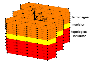
In Fig. 1 a tight-binding model of a ferromagnet-insulator-topological insulator (FITI) junction is shown. The topological insulator is modeled by the Hamiltonian Eq. (1), which we Fourier-transform perpendicular to the junction plane into real space onto its lattice. For the in-plane directions we assume periodic boundary conditions, allowing us to keep the in-plane momentum components (e.g. and for a -surface) as good quantum numbers. The ferromagnet (FM) is modeled as a metal with two spin-split subbands. For that purpose we use the same Hamiltonian Eq. (1) with parameters and corresponding to a 3 eV bandwidth. Additionally we add an exchange field of strength of the form
| (4) |
with and , which can be polarized in arbitrary direction . Choosing , states with one spin orientation reside at the Fermi surface, while those with opposite orientation are shifted to higher energies. This corresponds to a 100% spin polarization of the ferromagnet. A reduced spin polarization of the ferromagnet is handled by a superposition of two calculations with opposite polarity of the exchange field, as discussed in Appendix A. The insulating barrier is modeled by a tunneling Hamiltonian of the form
| (5) |
where creates an electron in orbital with spin in the top layer of the topological insulator and destroys an electron in the bottom layer of the ferromagnet. Here, and are the momentum components perpendicular to the junction plane. For the numerical calculations we have chosen a small hopping matrix element of , however, the relative TMR values calculated below do not depend on this choice.
Due to the structure of the Hamiltonian Eq. (1) topological surface states appear on the topological insulator side of the junction. The dispersion of the surface states forms a Dirac cone, which is hexagonally warped due to the third order terms Eq. (2) and (3). Fu2 Note that the position of the Dirac point and the shape of the Dirac cone depends on the surface direction. The surface states are spin-polarized with the direction of the spin helically winding around the Dirac cone. The spin-polarized tunneling current through the barrier thus flows off into different directions in the topological insulator depending on the polarization of the ferromagnet. In particular the direction of the current in the topological insulator can be controlled by rotation of the exchange field in the ferromagnet. This effect can be used to construct a TMR device from such a junction.
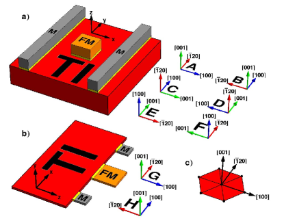
Possible setups for such devices are shown in Fig. 2. The spin-polarized current that is injected via a ferromagnetic electrode (FM) into the topological surface states can be extracted through metallic electrodes (M) at opposite positions on the same surface. For a given bias voltage the current through the two metallic electrodes will differ in strength due to the spin-momentum locking of the surface states. This leads to different resistances with respect to the ferromagnetic electrode, because the spin direction of the tunneling electrons will favor current flow to one of the two metallic electrodes. The resistances will vary with the direction of the exchange field in the ferromagnet resulting in a directional dependence of the resistance on the magnetization, i.e. a TMR effect. Due to the anisotropy of Bi2Se3 we study six setups for a three-dimensional (3D) device (A-F) and two for a two-dimensional (2D) device (G, H) as shown in Fig. 2, which may yield different TMR ratios. These setups differ in the crystallographic orientation of the topological insulator relative to the junction plane. In the 3D cases we investigate the three clean surfaces in -, - and -direction with two orthogonal arrangements of the metallic electrodes each. The 2D case could be realized by a thin film strip contacted at the edges, i.e. with an experimentally more complex arrangement. For that purpose, the film thickness should be less than 6 nm (6 quintuple layers) in order to ensure that the top and bottom surface states become sufficiently hybridized. YiZhang On the other hand the film thickness should be at least 1.5 nm to avoid that the material becomes topologically trivial. PD Here, we consider a film thickness of 3 nm to stay within these two limits. In this case the parameter needs to be reduced to an effective 2D value of , as has been discussed in Ref. PD, . In the 2D case we do not consider thin films grown along - or -direction as these are technically difficult to realize. In the following, the cartesian coordinates are tied to the geometry of the devices, while the orientation of the crystal in these devices is expressed by Miller indices, as indicated in Fig. 2. Hence, is always the momentum perpendicular to the surface plane and and are the in-plane momenta with pointing from the junction towards the metallic electrode. Note, that this definition of the cartesian coordinates only in the case of setup A coincides with that in Eq. (1) and (4).
The tunneling current through the insulating barrier is calculated using Fermi’s golden rule
| (6) |
which gives the transition rate from an initial state into a final state . Here, is the tunneling Hamiltonian Eq. (5) of the insulating barrier. Prange For a given bias voltage between the ferromagnetic electrode and the topological insulator, the total tunneling current is given by the expression Mahan
| (7) | |||||
Here, the sum runs over all eigenstates and of the ferromagnet and the topological insulator. The Fermi function
| (8) |
takes into account the occupation of the eigenstates at finite temperature. Differentiating with respect to leads to the differential conductance
| (9) | |||||
which is used to define the TMR ratio
| (10) |
Here, and define the direction of the exchange field Eq. (4) and is the maximal differential conductance with respect to one metallic electrode obtained when the exchange field and the polarization of the surface electrons with propagation direction perpendicular to that electrode are parallel. The maximal TMR ratio can then be obtained by rotating the exchange field by into the antiparallel orientation or, because of the spin-momentum locking of the TI surface states, by comparing the differential conductances with respect to both metallic electrodes (see Fig. 2). To calculate the differential conductance with respect to the different metallic electrodes, we sum only over those eigenstates of the TI with a positive group velocity component in the direction of the electrodes for one electrode and over those with a negative group velocity component for the opposite electrode.
III Results

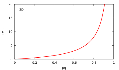
In this section we present our results for the TMR ratio in Bi2Se3 based on numerical calculations as well as an analytical approximation. The analytical approximation is derived in Appendix A. It assumes isotropic helical surface states and neglects the influence of bulk states. This should be a good approximation for bias voltages chosen within the bulk gap of the material in the vicinity of the Dirac point. While the numerical calculations give an exact solution based on Hamiltonian Eq. (1) including the influence of the bulk states, the analytical approximation gives a formula depending on the spin-polarization of the topological surface states. Here, is the average magnitude of the spin expectation value in the vicinity of the Dirac point. The analytical formula is useful as it provides a quick estimate of the TMR ratio and can be used for different materials once the spin-polarization of the surface states is known. Depending on the dimensionality of the device the formulas for the TMR ratio are slightly different, but independent of temperature and bias voltage (see Appendix A):
| (11) |
| (12) |
Here, is the spin-polarization of the ferromagnet. The angle is the in-plane polarization angle of the exchange field. The maximal TMR ratio is reached after a rotation of the exchange field () and is shown as a function of in Fig. 3. It is limited to for a 3D device while it diverges in the 2D case for . The factor in the denominator of Eq. (11) as compared with Eq. (12) comes from the fact that the two-dimensional manifold of surface states on the 3D devices possesses in-plane spin polarizations of all directions, as shown in Appendix A. Even for surface states with a finite amount of electrons can thus tunnel into surface states with a velocity component into the opposite direction, reducing the TMR ratio. In the 2D devices such a situation can be avoided.
For the numerical TMR ratios we calculate the eigenstates and eigenenergies of the TI by an exact diagonalization of the Fourier-transformed Hamiltonian on a lattice of size for setups A and B, for C-F, and for G and H, where the first number is always for the direction perpendicular to the surface plane. Due to the periodic boundary conditions within the surface plane this can be done separately for all discrete in-plane momenta . To obtain the sign of the group velocity component we compare the eigenenergies with those we get after a small variation of . Assuming the FM to be large, the spatial dependence of the FM states perpendicular to the surface is given by , where is the lattice position and the perpendicular momentum is a continuous function of the in-plane momentum and the TI eigenenergies, satisfying energy and in-plane momentum conservation (see Appendix A). To obtain the direction of the magnetization of the ferromagnet is chosen such that the differential conductance is maximized. This occurs, when the magnetization direction fits the expectation value of the spin operators Silvestrov of those TI surface states that propagate towards a metallic electrode. The TMR ratio is then calculated using Eq. (10), where the maximal and minimal differential conductances are calculated by summing only over those states with positive or negative group velocity component in Eq. (9), i.e. by looking at opposite metallic electrodes.
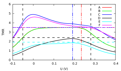
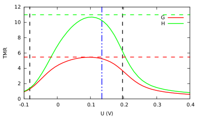
In Fig. 4 the results of these calculations at room temperature are shown (solid lines) in comparison with the corresponding expectation from the analytical approximation (horizontal dashed lines with the same color). The FM is chosen to be ideal for these calculations, i.e. fully polarized (). To make an appropriate comparison of our numerical results with the analytical approximation we have determined the polarization of the TI surface states from the numerical calculation in the following way: we determine from the absolute value of the spin expectation value for a surface state having a momentum in the direction of the metallic electrode close to the Dirac point. As the magnetization of the ferromagnet is aligned to the spin of this state, the analytical formula gives the best approximation for this value of , because the main contribution to the differential conductance comes from electrons with similar spin direction. Note, that the value of depends on the crystallographic orientation of the surface leading to different values for the different setups.
Since the surface states only exist inside the bulk gap and the bulk states are unpolarized, the TMR ratio drops towards the edges of the gap (shown by the vertical black lines). This influence of the bulk states increases with increasing temperature and may reduce the maximal TMR ratio in systems with small gaps. Taking a closer look at the different setups, setup A and B show nearly no difference and are in very good agreement with the analytical approximation for . There is only a tiny deviation for larger , where the numerical TMR ratio decreases due to a small albeit increasing out-of-plane polarization of the surface states caused by hexagonal warping.
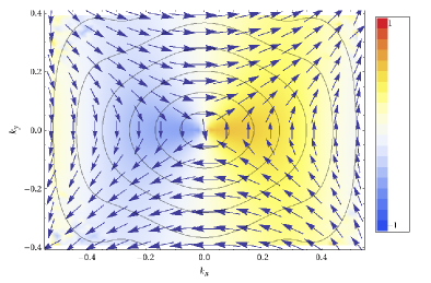
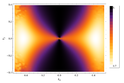
Because of the anisotropy of the and surfaces, the analytical approximation gives only a rough estimate for the TMR ratio of setups C-F. The anisotropy changes the shape of the Dirac cone and with it the spin orientation from circular to a more elliptical form (see Fig. 5). This creates an imbalance in the tunneling probabilities of electrons with different spin orientations. For setups C and F the TMR ratio at the Dirac point is slightly larger than the estimated 3.5 and rises up to for setup C and for setup F near the lower edge of the bulk gap. As the TMR ratio increases away from the Dirac point, it is limited by the size of the bulk gap and the position of the Dirac point inside the gap. The fact that setup C reaches a larger value than setup F indicates that for equally polarized surfaces it is beneficial to choose the surface parallel to a crystal axis.
In contrast to setups C and F, the anisotropy reduces the TMR ratio for setups D and E, which is already smaller because the surface states have a reduced spin-polarization of and near the Dirac point, respectively. The TMR ratio is further reduced by a change in the polarization orientation and strength as a function of energy away from the Dirac point.
In the case of a 2D device (setup G and H), the TMR ratio reaches much larger values than in the 3D case, as there are basically only two spin orientations flipping at . Near the Dirac point, the TMR ratio now falls somewhat below the analytical approximation and decreases rapidly towards the edges of the gap. On one hand this is due to the higher sensitivity of the larger TMR ratios resulting in a more important influence of the bulk states. On the other hand, similar as for setup D and E, there is a change in the orientation and strength of the spin polarization as a function of energy, further reducing the TMR ratio away from the Dirac point. Still we get a maximal TMR ratio of for setup G () and for setup H () at room temperature.
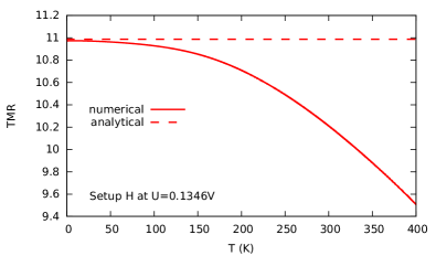
In Fig. 6 we show the temperature dependence of the TMR ratio for setup H and bias voltage chosen at the Dirac point. Here, it is seen that the value of the analytical approximation is reached at low temperatures. This result demonstrates that the finite temperature occupation of the bulk states somewhat mitigates the TMR ratio already at room temperature in the 2D devices.
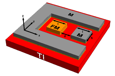
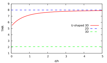
The 2D devices (setup G and H) reach much larger TMR values than the 3D ones. However, they are technically more challenging to realize as the tunneling barrier has to be attached to the edge states of a thin TI film. In Fig. 7 we propose an alternative 3D device, which is easier to realize than the 2D devices, however, approaches the same large TMR values. In this device one of the two metallic electrodes is U-shaped and is supposed to capture most electrons that do not propagate in positive -direction from the ferromagnetic to the other, smaller metallic electrode. As a result, the electrons that reach the smaller metallic electrode preferentially possess only a single spin orientation. Thus, the transport between the ferromagnetic and the smaller metallic electrode approaches a one-dimensional transport, similarly as in the edge states of the 2D devices. We have applied our analytical approximation to this geometry (for more details see Appendix A), corresponding to a surface, i.e. the crystallographic orientation of setup A. In Fig. 8 the TMR ratio of this U-shaped device is shown as function of the ratio , where is the distance between the ferromagnetic and the smaller metallic electrode, and is the height of the electrodes as shown in Fig. 7. In this calculation we assumed that the ferromagnetic and the smaller metallic electrode are square-shaped, i.e. . For illustration, we assumed that the product of the polarizations of the ferromagnet and the topological insulator is 0.8. As Fig. 8 shows, the U-shaped 3D device yields much larger TMR values than the 3D devices. For the TMR ratio of the U-shaped device approaches the TMR ratio of the 2D device, which is clear as with increasing distance the angular range of topological surface states that can reach the metallic electrode is gradually reduced and focused.
The calculations we reported here were done with parameters appropriate for undoped Bi2Se3, as pointed out above. However, in practice these materials often appear to be intrisically doped, Xia ; Hsieh2 which shifts the Fermi level with respect to the surface Dirac cone. For Bi2Se3 a Fermi level shift of 200 meV has been reported. Xia We want to point out that the functionality of the devices proposed here is not affected by such intrinsic doping. The Fermi level shift will shift the energies of the topological surface states with respect to the ones of the ferromagnet. This energy shift can be fully compensated for by a shift of the bias voltage in Eq. (9). This will lead to a bias voltage shift of our results in Fig. 4. Thus the high TMR ratios will be robust against intrinsic doping, but just appear at a shifted bias voltage.
While our calculations find a full spin-polarization for the z-surface, consistent with recent spin- and angle-resolved photoemission spectroscopy (SARPES) measurements of Pan et alPan:PRB88 , the spin-polarization in Bi2Se3 is still controversial. The reported spin-polarization ranges from 50%-65% in first principle calculations Yazyev ; Wang ; Sanchez to 75%-80% or more in SARPES measurements Pan:PRL106 ; Jozwiak . If we consider these values, according to Fig. 3 the TMR ratio could be reduced to in the 3D devices and in the 2D devices, which is still large, though.
As our analytical formulas for the TMR ratio Eq. (11) and (12) depend only on the spin-polarization and not on the exact parametrization they are universally valid for all materials in the limit of an isotropic surface. In contrast, the TMR ratio for an anisotropic surface strongly depends on the model parameters and the deviation from the isotropic solution may therefore be different for other materials.
In the present work we are focussing on Bi2Se3, which has been studied well in the past. Considering other materials, TlBiSe2 could also be a good candidate for TMR devices as discussed here, because it has an in-plane spin-polarization of %, a negligible out-of-plane polarization and a large bulk gap of eV. Souma:PRL109 ; Souma:PRL106 ; Sato The high spin polarization of 80%-90% of Sb2Te3 promises a high TMR ratio, too. However, at room temperature it will probably be reduced because of the small bulk gap of only .Pauly Bi2Te3 and Pb(Bi,Sb)2Te4 seem to be less attractive since they have in-plane spin-polarizations of only 45%-60% Yazyev ; Herdt ; Souma:PRL106 ; Scholz and 50%Nomura and small bulk gaps of only Yazyev ; Chen and Souma:PRL108 ; Kuroda , respectively. They also possess a significant out-of-plane polarization due to the hexagonal deformation of the Fermi surface. Yazyev ; Souma:PRL106 ; Herdt ; Nomura
An attractive feature of the devices proposed here is the topological protection of the spin-locked surface states, which makes them particularly robust against perturbations. In usual TMR junctions defects close to the interface can substantially suppress the TMR ratio in particular at high temperature. Yamamoto ; Drewello For the present devices we have to distinguish non-magnetic and magnetic scattering mechanisms. Non-magnetic scattering processes, like disorder or faceting of the barrier, which scatter the momentum of an electron during the transfer from the ferromagnet to the topological insulator, but keep its spin conserved, are only weakly affecting our TMR results. This is because the TMR ratio is predominantly dictated by the helical spin structure of the surface states, which is topologically protected. As long as the spin is conserved, momentum scattering is not changing our results as the total current already consists of contributions from all momentum directions. Magnetic scattering mechanisms, on the other hand, do reduce the TMR ratio. This is obvious, as a spin-flip process during tunneling will change the direction of flow in the topological surface state. Such processes could be modeled by a reduced apparent polarization of the ferromagnet seen by the topological insulator. An experimental realization of our devices should thus take care to avoid magnetic scattering in the barrier. These are the same quality requirements as for conventional TMR devices based on magnetic tunnel junctions and has been successfully dealt with in the past, however.
The distance between the electrodes should be chosen sufficiently small such that electrons travelling from the ferromagnetic electrode to one metallic electrode are not back-scattered to the opposite metallic electrode inbetween. As the surface states are topologically protected by time-reversal symmetry, such back-scattering is strongly suppressed and can only occur when time-reversal symmetry breaking scattering impurities or imperfections exist in the topological insulator. Thus, the distance between the electrodes should be smaller than the spin-flip mean-free-path of the surface states. Values of the order of 2 m have been reported. Koenig1 ; Koenig2 It has been demonstrated in the past that magnetic tunnel junctions can be structured down to a 50 nanometer scale. Kubota
In conventional semiconductor Rashba devices TMR ratios of up to 50% have been reached at room temperature. Wojcik ; Yoh For TMR devices based on magnetic tunnel junctions with two ferromagnetic electrodes reported TMR ratios range between 180% and 600%. Yamamoto ; Drewello ; Parkin ; Yuasa ; Ikeda ; Liu The TMR values calculated here are comparable or larger than these values.
IV Summary and Conclusions
In the present work we proposed specific setups to build TMR devices exploiting the topological insulator material Bi2Se3. Using a realistic tight-binding model we calculated the achievable TMR ratios as a function of bias voltage and temperature. If the bias voltage is chosen properly, we find that room temperature TMR ratios of 490 % can be achieved in the 3D devices and 1070 % in the 2D devices. We suggested a U-shaped 3D device, which is experimentally easier to realize than the 2D devices, but reaches correspondingly high TMR values. We derived simple analytical formulas for the devices, which provide a quick approximate figure of merit once the surface state polarization of a given topological insulator is known. For the 3D devices we have shown that on an anisotropic surface the TMR ratio may become larger than the one estimated from the analytical formula. In contrast to conventional TMR devices the devices proposed here do not need a second ferromagnetic layer, as an intrinsic magnetic reference direction is already provided by the topological insulator. In addition, the present devices provide a means to experimentally probe the surface state polarization of a given topological insulator.
Appendix A Analytical TMR Ratio
In this appendix we derive an analytical approximation for the TMR ratio. We base this on an analytical approximation of the surface states only and neglect the effects of bulk states. Considering the large bulk gap of Bi2Se3, this should be a good approximation even at room temperature.
To find an analytical approximation of the surface states for a surface at , we expand Hamiltonian Eq. (1) up to second order in . As a starting point we first neglect all - and -dependent terms by setting . If we assume the TI to be half infinite with its boundary at , we have to replace with the momentum operator and search for nontrivial solutions that vanish both at and for . There exist two degenerate eigenstates with energy satisfying both conditions:
| (17) | |||||
| (22) |
with , and some normalization constant for the -dependent part. Next we treat the neglected - and -dependent terms as a perturbation using degenerate perturbation theory and get the new surface states
| (23) |
with
The perturbed eigenenergies are
| (26) |
Here, and and is for the upper and lower Dirac cone, respectively. If we expand , and up to second order in und , the solutions become isotropic in the --plane and we can write solely as a function of and the in-plane polar angle . The energies then become
| (27) |
and thus only depend on the magnitude . This expression agrees with the one derived previously in Ref. Shan, .
Calculation of the expectation values of the spin operators Silvestrov shows that the spin of these surface states is always perpendicular to the in-plane momentum and lies within the surface plane. As the direction of the spin is the same for both orbitals, this model yields surface states which are fully polarized, at least at the -surface. Here, we allow for a finite spin polarization and thus rewrite the surface state wave functions as a function of polarization
| (28) |
As all constant prefactors cancel in the TMR ratio we neglect these as well as the spatial dependence, because in the calculation of the tunneling current only the lattice position next to the barrier plays a role. The spatial dependence of the FM states perpendicular to the surface is a superposition of an incoming plane wave with the reflected one having a node inside the barrier (at ) and is thus given by . Note that this is an exact solution of the tight-binding model for a thick FM with zero transmission probability through the barrier. Here, the momentum is a continuous function of the in-plane momentum and the TI eigenenergies , satisfying energy and in-plane momentum conservation:
| (29) |
Since the spin of the surface states lies within the surface plane it is sufficient to write the states of the FM as a function of the in-plane polar angle
| (30) |
The transfer matrix elements
| (31) |
can then be inserted into Eq. (9).
In the calculation of the differential conductance the geometry of the device can be accounted for by an additional angular dependent factor . This factor describes the probability that an electron starting its propagation in the TI at an angle below the FM electrode ends up at the metallic electrode at averaged over the spatial extend of the two electrodes. Under the assumption that , which holds for a device which is mirror symmetric with respect to the --plane and valid for all devices considered in this work, the -integral can be separated from the rest of the differential conductance
with the function
which is independent of .
Up to this point we considered an ideal FM, i.e. fully polarized. To account for a finite polarization of the FM we have to replace by
Here, with is the relative density of states of electrons in the FM with spin projection parallel (+) or antiparallel (-) to the polarization angle . Defining
| (35) |
the TMR ratio
| (36) |
only depends on , and . In particular it does not depend on temperature, because the temperature dependence of the differential conductance is the same in all directions due to the in-plane rotational symmetry of the surface states and thus drops out in the TMR ratio. This temperature independence is lost of course, if the contribution of the bulk states is included. The geometry of the device only appears via the single parameter . This parameter can now be calculated for different geometries of the devices. For setups A-H we assume that all electrons initially moving in positive -direction end up at the electrode at and all others at the counterelectrode. For the 3D devices A-F the function is then simply given by
| (37) |
which yields . For the 2D devices G and H we have
| (38) |
giving .
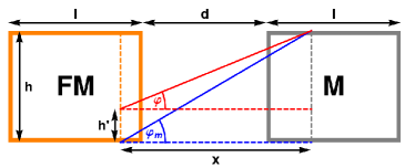
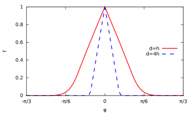
For the device shown in Fig. 7 we can derive from the sketch shown in Fig. 9. Considering an electron starting from the FM at an angle on a vertical line with distance from a vertical line in the metallic electrode (M), it can only reach that line if it comes from the fraction , i.e. the mean probability to reach the line is if and otherwise zero. Averaging over the length of the FM and the metallic electrode results in
where is the Heaviside step function. can then be calculated numerically for specific values of , and . In Fig. 10 this function is shown for and as well as , showing that for larger value of the angular dependence becomes more strongly focused near .
References
- (1) B. A. Bernevig, T. L. Hughes, and S.-C. Zhang, Quantum Spin Hall Effect and Topological Phase Transition in HgTe Quantum Wells, Science 314, 1757 (2006).
- (2) L. Fu, C. L. Kane and E. J. Mele, Topological Insulators in Three Dimensions, Phys. Rev. Lett. 98, 106803 (2007).
- (3) M. König, S. Wiedmann, C. Brüne, A. Roth, H. Buhmann, L.W. Molenkamp, X.-L. Qi, and S.-C. Zhang, Quantum Spin Hall Insulator State in HgTe Quantum Wells Science 318, 766 (2007).
- (4) D. Hsieh, D. Qian, L. Wray, Y. Xia, Y. Hor, R.J. Cava, and M.Z. Hasan, A topological Dirac insulator in a quantum spin Hall phase, Nature (London) 452, 970 (2008).
- (5) Y. L. Chen, J. G. Analytis, J.-H. Chu, Z. K. Liu, S.-K. Mo, X. L. Qi, H. J. Zhang, D. H. Lu, X. Dai, Z. Fang, S. C. Zhang, I. R. Fisher, Z. Hussain, and Z.-X. Shen, Experimental Realization of a Three-Dimensional Topological Insulator, Bi2Te3, Science 325, 178 (2009).
- (6) Y. Xia, D. Qian, D. Hsieh, L. Wray, A. Pal, H. Lin, A. Bansil, D. Grauer, Y. S. Hor, R. J. Cava, and M. Z. Hasan, Observation of a large-gap topological-insulator class with a single Dirac cone on the surface, Nature Phys. 5, 398 (2009).
- (7) D. Hsieh, Y. Xia, D. Qian, L. Wray, F. Meier, J.H. Dil, J. Osterwalder, L. Patthey, A.V. Fedorov, H. Lin, A. Bansil, D. Grauer, Y.S. Hor, R.J. Cava, and M.Z. Hasan, Observation of Time-Reversal-Protected Single-Dirac-Cone Topological-Insulator States in Bi2Te3 and Sb2Te3, Phys. Rev. Lett. 103, 146401 (2009).
- (8) K. Kuroda, H. Miyahara, M. Ye, S. V. Eremeev, Yu. M. Koroteev, E. E. Krasovskii, E. V. Chulkov, S. Hiramoto, C. Moriyoshi, Y. Kuroiwa, K. Miyamoto, T. Okuda, M. Arita, K. Shimada, H. Namatame, M. Taniguchi, Y. Ueda, and A. Kimura, Experimental Verification of PbBi2Te4 as a 3D Topological Insulator, Phys. Rev. Lett. 108, 206803 (2012).
- (9) Y. Ando, Topological Insulator Materials, J. Phys. Soc. Japan 82, 102001 (2013).
- (10) D. Hsieh, Y. Xia, D. Qian, L. Wray, J. H. Dil, F. Meier, J. Osterwalder, L. Patthey, J. G. Checkelsky, N. P. Ong, A. V. Fedorov, H. Lin, A. Bansil, D. Grauer, Y. S. Hor, R. J. Cava, and M. Z. Hasan, A tunable topological insulator in the spin helical Dirac transport regime, Nature (London) 460, 1101 (2009).
- (11) C. Brüne, A. Roth, H. Buhmann, E. M. Hankiewicz, L. W. Molenkamp, J. Maciejko, X.-L. Qi and S.-C. Zhang, Spin polarization of the quantum spin Hall edge states, Nature Phys. 8, 485 (2012).
- (12) Z.-H. Pan, E. Vescovo, A. V. Fedorov, D. Gardner, Y. S. Lee, S. Chu, G. D. Gu, and T. Valla, Electronic Structure of the Topological Insulator Bi2Se3 Using Angle-Resolved Photoemission Spectroscopy: Evidence for a Nearly Full Surface Spin Polarization, Phys. Rev. Lett. 106, 257004 (2011).
- (13) Y. Tanaka, T. Yokoyama, and N. Nagaosa, Manipulation of the Majorana Fermion, Andreev Reflection, and Josephson Current on Topological Insulators, Phys. Rev. Lett. 103, 107002 (2009).
- (14) S. Mondal, D. Sen, K. Sengupta, and R. Shankar, Tuning the Conductance of Dirac Fermions on the Surface of a Topological Insulator, Phys. Rev. Lett. 104, 046403 (2010).
- (15) J. Linder, Y. Tanaka, T. Yokoyama, A. Sudbo, and N. Nagaosa, Unconventional Superconductivity on a Topological Insulator, Phys. Rev. Lett. 104, 067001 (2010).
- (16) I. Garate and M. Franz, Inverse Spin-Galvanic Effect in the Interface between a Topological Insulator and a Ferromagnet, Phys. Rev. Lett. 104, 146802 (2010).
- (17) T. Yokoyama, Y. Tanaka, and N. Nagaosa, Anomalous magnetoresistance of a two-dimensional ferromagnet/ferromagnet junction on the surface of a topological insulator, Phys. Rev. B 81, 121401 (2010).
- (18) A.M. Black-Schaffer and J. Linder, Majorana fermions in spin-orbit-coupled ferromagnetic Josephson junctions, Phys. Rev. B 84, 180509(R) (2011).
- (19) V. Krueckl and K. Richter, Switching Spin and Charge between Edge States in Topological Insulator Constrictions, Phys. Rev. Lett. 107, 086803 (2011).
- (20) B. D. Kong, Y. G. Semenov, C. M. Krowne, and K. W. Kim, Unusual magnetoresistance in a topological insulator with a single ferromagnetic barrier, Appl. Phys. Lett. 98, 243112 (2011).
- (21) M. Salehi, M. Alidoust, Y.Rahnavard, G.Rashedi, In-plane magnetoresistance on the surface of topological insulator Physica E 43, 966 (2011).
- (22) R. Vali and M. Vali, Tunneling conductance and magnetoresistance in topological insulator Fi/I/Fi/d-wave superconductor junctions, J. Appl. Phys. 112, 103919 (2012).
- (23) T. Paananen, H. Gerber, M. Götte, and T. Dahm, Appearance of flat surface bands in three-dimensional topological insulators in a ferromagnetic exchange field, New J. Phys. 16, 033019 (2014).
- (24) K. Taguchi, T. Yokoyama, and Y. Tanaka, Giant magnetoresistance in the junction of two ferromagnets on the surface of diffusive topological insulators, Phys. Rev. B 89, 085407 (2014).
- (25) R. Li, J. Wang, X.-L. Qi, and S.-C. Zhang, Dynamical axion field in topological magnetic insulators, Nature Phys. 6, 284 (2010).
- (26) H. Zhang, C.-X. Liu, X.-L. Qi, X. Dai, Z. Fang, and S.-C. Zhang, Topological insulators in Bi2Se3, Bi2Te3 and Sb2Te3 with a single Dirac cone on the surface, Nature Phys. 5, 438 (2009).
- (27) W.-Y. Shan, H.-Z. Lu, and S.-Q. Shen, Effective continuous model for surface states and thin films of three-dimensional topological insulators, New J. Phys. 12, 043048 (2010).
- (28) C.-X. Liu, X.-L. Qi, H.J. Zhang, X. Dai, Z. Fang, and S.-C. Zhang, Model Hamiltonian for topological insulators, Phys. Rev. B 82, 045122 (2010).
- (29) L. Hao and T. K. Lee, Surface spectral function in the superconducting state of a topological insulator, Phys. Rev. B 83, 134516 (2011).
- (30) L. Fu, Hexagonal Warping Effects in the Surface States of the Topological Insulator Bi2Te3 Phys. Rev. Lett. 103, 266801 (2009).
- (31) H. Okamoto, The Bi-Se (Bismuth-Selenium) System, J. Phase Equilib. 15, 195 (1994).
- (32) H. Lind, S. Lidin, and U. Häussermann, Structure and bonding properties of (Bi2Se3)m(Bi2)n stacks by first-principles density functional theory, Phys. Rev. B 72, 184101 (2005).
- (33) G. Zhang, H. Qin, J. Teng, J. Guo, Q. Guo, X. Dai, Z. Fang, and K. Wu, Quintuple-layer epitaxy of thin films of topological insulator Bi2Se3, Appl. Phys. Lett. 95, 053114 (2009).
- (34) Yi Zhang et al., Crossover of the three-dimensional topological insulator Bi2Se3 to the two-dimensional limit, Nature Phys. 6, 584 (2010).
- (35) T. Paananen and T. Dahm, Magnetically robust topological edge states and flat bands, Phys. Rev. B 87, 195447 (2013).
- (36) R.E. Prange, Tunneling from a Many-Particle Point of View, Phys. Rev. 131, 1083 (1963).
- (37) G. D. Mahan, Many-Particle Physics, (2nd ed, Plenum Press, New York 1990).
- (38) P. G. Silvestrov, P. W. Brouwer, and E. G. Mishchenko, Spin and charge structure of the surface states in topological insulators, Phys. Rev. B 86, 075302 (2012).
- (39) Z.-H. Pan, E. Vescovo, A. V. Fedorov, G. D. Gu, and T. Valla, Persistent coherence and spin polarization of topological surface states on topological insulators, Phys. Rev. B 88, 041101(R) (2013).
- (40) O. V. Yazyev, J. E. Moore, and S. G. Louie, Spin Polarization and Transport of Surface States in the Topological Insulators Bi2Se3 and Bi2Te3 from First Principles, Phys. Rev. Lett. 105, 266806 (2010).
- (41) X. Wang, G. Bian, T. Miller, and T.-C. Chiang, Topological spin-polarized electron layer above the surface of Ca-terminated Bi2Se3, Phys. Rev. B 87, 035109 (2013).
- (42) J. Sánchez-Barriga et al, Photoemission of Bi2Se3 with Circularly Polarized Light: Probe of Spin Polarization or Means for Spin Manipulation?, Phys. Rev. X 4, 011046 (2014).
- (43) C. Jozwiak, Y. L. Chen, A. V. Fedorov, J. G. Analytis, C. R. Rotundu, A. K. Schmid, J. D. Denlinger, Y.-D. Chuang, D.-H. Lee, I. R. Fisher, R. J. Birgeneau, Z.-X. Shen, Z. Hussain, and A. Lanzara, Widespread spin polarization effects in photoemission from topological insulators, Phys. Rev. B 84, 165113 (2011).
- (44) S. Souma, M. Komatsu, M. Nomura, T. Sato, A. Takayama, T. Takahashi, K. Eto, K. Segawa, and Y. Ando, Spin Polarization of Gapped Dirac Surface States Near the Topological Phase Transition in TlBi(S1-xSex)2, Phys. Rev. Lett. 109, 186804 (2012).
- (45) S. Souma, K. Kosaka, T. Sato, M. Komatsu, A. Takayama, T. Takahashi, M. Kriener, K. Segawa, and Y. Ando, Direct Measurement of the Out-of-Plane Spin Texture in the Dirac-Cone Surface State of a Topological Insulator, Phys. Rev. Lett. 106, 216803 (2011).
- (46) T. Sato, K. Segawa, H. Guo, K. Sugawara, S. Souma, T. Takahashi, and Y. Ando, Direct Evidence for the Dirac-Cone Topological Surface States in the Ternary Chalcogenide TlBiSe2, Phys. Rev. Lett. 105, 136802 (2010).
- (47) C. Pauly, G. Bihlmayer, M. Liebmann, M. Grob, A. Georgi, D. Subramaniam, M. R. Scholz, J. Sánchez-Barriga, A. Varykhalov, S. BlÌgel, O. Rader, and M. Morgenstern, Probing two topological surface bands of Sb2Te3 by spin-polarized photoemission spectroscopy, Phys. Rev. B 86, 235106 (2012).
- (48) A. Herdt, L. Plucinski, G. Bihlmayer, G. Mussler, S. Döring, J. Krumrain, D. Grützmacher, S. Blügel, and C. M. Schneider, Spin-polarization limit in Bi2Te3 Dirac cone studied by angle- and spin-resolved photoemission experiments and ab initio calculations, Phys. Rev. B 87, 035127 (2013).
- (49) However, a spin polarization of 75%-80% in Bi2Te3 has been reported in M. R. Scholz et al, Reversal of the Circular Dichroism in Angle-Resolved Photoemission from Bi2Te3, Phys. Rev. Lett. 110, 216801 (2013).
- (50) M. Nomura, S. Souma, A. Takayama, T. Sato, T. Takahashi, K. Eto, K. Segawa, and Y. Ando, Relationship between Fermi surface warping and out-of-plane spin polarization in topological insulators: A view from spin- and angle-resolved photoemission, Phys. Rev. B 89, 045134 (2014).
- (51) S. Souma, K. Eto, M. Nomura, K. Nakayama, T. Sato, T. Takahashi, K. Segawa, and Y. Ando, Topological Surface States in Lead-Based Ternary Telluride Pb(Bi1-xSbx)2Te4, Phys. Rev. Lett. 108, 116801 (2012).
- (52) M. Yamamoto, T. Ishikawa, T. Taira, G.-F. Li, K. Matsuda, T. Uemura, Effect of defects in Heusler alloy thin films on spin-dependent tunnelling characteristics of Co2MnSi/MgO/Co2MnSi and Co2MnGe/MgO/Co2MnGe magnetic tunnel junctions , J. Phys.: Condens. Matter 22 164212 (2010).
- (53) V. Drewello, D. Ebke, M. Schäfers, Z. Kugler, G. Reiss, A. Thomas, Magnon excitation and temperature dependent transport properties in magnetic tunnel junctions with Heusler compound electrodes, J. Appl. Phys. 111, 07C701 (2012).
- (54) M. König, H. Buhmann, L. W. Molenkamp, T. Hughes, C.-X. Liu, X.-L. Qi, and S.-C. Zhang, The Quantum Spin Hall Effect: Theory and Experiment J. Phys. Soc. Japan 77, 031007 (2008).
- (55) M. König, M. Baenninger, A. G. F. Garcia, N. Harjee, B. L. Pruitt, C. Ames, P. Leubner, C. Brüne, H. Buhmann, L. W. Molenkamp, and D. Goldhaber-Gordon, Spatially Resolved Study of Backscattering in the Quantum Spin Hall State, Phys. Rev. X 3, 021003 (2013).
- (56) H. Kubota, Y. Ando, T. Miyazaki, G. Reiss, H. Brückl, W. Schepper, J. Wecker, G. Gieres, Size dependence of switching field of magnetic tunnel junctions down to 50 nm scale, J. Appl. Phys. 94, 2028 (2003).
- (57) P. Wójcik, J. Adamowski, B. J. Spisak, and M. Wooszyn, J. Appl. Phys. 115, 104310 (2014).
- (58) K. Yoh, Z. Cui, K. Konishi, M. Ohno, K. Blekker, W. Prost, F.-J. Tegude, and J.-C. Harmand, An InAs Nanowire Spin Transistor with Subthreshold Slope of 20mV/dec, Proceedings of IEEE 70th Annual Device Research Conference, p. 79 (2012).
- (59) S. S. Parkin, C. Kaiser, A. Panchula, P. M. Rice, B. Hughes, M. Samant, S.-H. Yang, Giant tunnelling magnetoresistance at room temperature with MgO (100) tunnel barriers, Nature Mater. 3, 862 (2004).
- (60) S. Yuasa, T. Nagahama, A. Fukushima, Y. Suzuki, K. Ando, Giant room-temperature magnetoresistance in single-crystal Fe/MgO/Fe magnetic tunnel junctions, Nature Mater. 3, 868 (2004).
- (61) S. Ikeda, J. Hayakawa, Y. Ashizawa, Y. M. Lee, K. Miura, H. Hasegawa, M. Tsunoda, F. Matsukura, and H. Ohno, Tunnel magnetoresistance of 604% at 300K by suppression of Ta diffusion in CoFeB/MgO/CoFeB pseudo-spin-valves annealed at high temperature, Appl. Phys. Lett. 93, 082508 (2008).
- (62) H.-X. Liu, Y. Honda, T. Taira, K. Matsuda, M. Arita, T. Uemura, M. Yamamoto, Giant tunneling magnetoresistance in epitaxial Co2MnSi/MgO/Co2MnSi magnetic tunnel junctions by half-metallicity of Co2MnSi and coherent tunneling, Appl. Phys. Lett. 101, 132418 (2012).