Band structure of silicene on the zirconium diboride (0001) thin film surface - convergence of experiment and calculations in the one-Si-atom Brillouin zone
Abstract
So far, it represents a challenging task to reproduce angle-resolved photoelectron (ARPES) spectra of epitaxial silicene by first-principles calculations. Here, we report on the resolution of the previously controversial issue related to the structural configuration of silicene on the ZrB2(0001) surface and its band structure. In particular, by representing the band structure in a large Brillouin zone associated with a single Si atom, it is found that the imaginary part of the one-particle Green’s function follows the spectral weight observed in ARPES spectra. By additionally varying the in-plane lattice constant, the results of density functional theory calculations and ARPES data obtained in a wide energy range converge into the “planar-like” phase and provide the orbital character of electronic states in the vicinity of the Fermi level. It is anticipated that the choice of a smaller commensurate unit cell for the representation of the electronic structure will be useful for the study of epitaxial two-dimensional materials on various substrates in general.
pacs:
73.22.-f, 68.43.Fg, 73.20.-rI Introduction
Silicene, the Si version of the two-dimensional carbon allotrope graphene, promises interesting electronic properties that derive from its graphene-like electronic structure, a large spin-orbit coupling and the out-of-plane buckling of atoms belonging to the two distinguishable sub-lattices.Liu et al. (2011); Ezawa (2012a); Takeda and Shiraishi (1994); Cahangirov et al. (2009); Lee et al. (2013a) As such, Dirac fermions at the Fermi level (),Takeda and Shiraishi (1994); Cahangirov et al. (2009) a large quantum spin Hall effect,Liu et al. (2011); Ezawa (2012a) a topological quantum phase transitionEzawa (2012b) and perfect spin filtering Tsai et al. (2013) are predicted to occur in its low-buckled, free-standing form. Importantly, as compared to graphene, under varying external conditions, silicene is structurally more flexible and can occur with a variety of lattice constants, atomistic structures and with a varying ratio.Lee et al. (2013a); Fleurence et al. (2012) This flexibility may allow tuning of the electronic propertiesFleurence et al. (2012); Wang and Ding (2013) to be adapted in useful applications.
While free-standing silicene is yet hypothetical, two-dimensional Si honeycomb lattices have recently been prepared on several metallic substrates such as Ag(111),Lin et al. (2012); Jamgotchian et al. (2012); Vogt et al. (2012) ZrB2(0001)Fleurence et al. (2012) and Ir(111)Meng et al. (2013) which opens the way for their systematic and comprehensive experimental characterization. The structural and electronic properties of epitaxial silicene phases are expected to be significantly altered from those of free-standing silicene, and are determined by the strength of hybridization with in particular the electronic states of the substrates and the resulting types of buckling.Lee et al. (2013a); Chen et al. (2012) Since this is a complex matter, not surprisingly, the interpretation of in particular observed surface reconstructionsLin et al. (2012); Jamgotchian et al. (2012); Vogt et al. (2012); Feng et al. (2012); Chiappe et al. (2012); Chen et al. (2013) and of the spectral features visible in angle-resolved photoelectron (ARPES) spectraFleurence et al. (2012); Vogt et al. (2012); Avila et al. (2013); Tsoutsou et al. (2013) have been and is still a matter of controversy.
In contrast to multiple epitaxial silicene phases observed by scanning tunneling microscopy (STM) on the Ag(111) surface, so far, only a single phase has been reported to be formed on the ZrB2(0001) surface.Fleurence et al. (2012) In this phase, ()-reconstructed silicene is in an epitaxial relationship to the () ZrB2(0001) unit cell. While evidence for atomic-scale buckling comes from photoelectron diffraction data,Fleurence et al. (2012) ARPES spectra show two upwards curved spectral features that approach by up to 250 meV at the () point of (unreconstructed) silicene and, owing to backfolding, are mirrored with weak intensity at the point in the Brillouin zone (BZ).Fleurence et al. (2012); Friedlein et al. (2013)
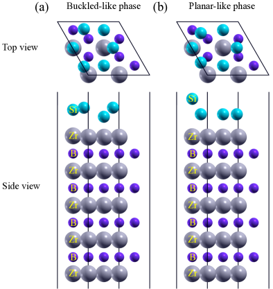
Density functional theory (DFT) calculations find two possible structures,Lee et al. (2013a) shown in Fig. 1, which so far only agree partially with the experimental data. In particular, while within DFT, a “planar-like” structure (Fig. 1 (b)) was reported to be the ground state of silicene on ZrB2(0001),Lee et al. (2013a) scanning tunneling spectroscopy (STS) spectra and photoelectron diffraction data could also be explained by the calculated electronic properties of the metastable, so called “buckled-like” phase (Fig. 1 (a)).Fleurence et al. (2012, 2014) Even more, so far, the band structure of both phases shows only partial agreement with ARPES spectra.Lee et al. (2013a) This has preliminary been attributed to the presence of long-range interactions leading to the spontaneous formation of stress domains within the two-dimensional layer of Si atoms.Fleurence et al. (2012)
In this context, another important issue that needs consideration is the sensitivity of the ARPES cross-section to the selected Brillouin zone.Dietz and Eastman (1978); Shirley et al. (1995) As such, the strong change of the graphene band intensity upon crossing the zone boundaryZhou et al. (2006); Bostwick et al. (2007) has initially been considered to derive from the dependence of the photoelectron emission matrix elements on the sign of the initial state electron momentumDietz and Eastman (1978) and has been discussed to be related to quantum mechanical interference between atoms in the two different sub-lattices.Shirley et al. (1995) In the case of epitaxial silicene on ZrB2(0001), Si atoms are not in two sub-lattices but occupy three distinguishable atomic sites.Fleurence et al. (2012); Friedlein et al. (2014) However, similar interference effects may occur.
In the present calculations, we have introduced a conceptual unit cell that contains only a single Si atom to allow interference between the distinguishable Si atoms defined in the () unit cell via the phase factors in terms of unfolding the electronic band structures.Ku et al. (2010); Lee et al. (2013b) By additionally varying slightly the in-plane lattice constant, we find good agreement between ARPES spectra obtained in a wide energy range and the calculated band structure of the planar-like phase, even without explicitly considering stress domains. The agreement allows for an analysis of the orbital character of the electronic states and reveals that the upwards curved bands which, according to ARPES data,Fleurence et al. (2012) approach at () point are formed by hybridization of Si and orbitals and contain contributions of Zr orbitals as well.
II Computational and Experimental
The DFT calculations within a generalized gradient approximation (GGA)Kohn and Sham (1965); Perdew et al. (1996) were performed using the OpenMX code based on norm-conserving pseudopotentials generated with multi reference energiesMorrison et al. (1993) and optimized pseudoatomic basis functions.Ozaki (2003); Ozaki et al. For each Zr atom, three, two, and two optimized radial functions were allocated for the -, -, and -orbitals, respectively, as denoted by . For both Si and B atoms, basis functions were adopted. The cut-off radius of 7 Bohr was chosen for all the basis functions. The regular mesh of 220 Ry in real space was used for the numerical integrations and for the solution of the Poisson equation. An () mesh of points was used to study an isolated slab consisting of five Zr, four B, and one silicene layers implemented by the effective screening medium method.Ohwaki et al. (2012) The force on each atom was relaxed to be less than 0.0001 Hartree/Bohr. The XCrySDen software was used to generate the figures.Kokalj (2003)
ARPES spectra were obtained using the SES-200 hemispherical analyzer at the end-station of the undulator beam line 13B at the Photon Factory synchrotron radiation facility, located at the High Energy Accelerator Research Organization (KEK), Tsukuba, Japan, using the photon energy of = 43 eV. The total energy resolution was better than 35 meV as determined from the broadening of . At this end-station, the electric field vector of the light was at the fixed angle of 25∘ with respect to the photoelectron analyzer.
Oxide-free silicene samples were prepared as described previously.Fleurence et al. (2012); Yamada-Takamura et al. (2010) Note that under optimal conditions,Yamada-Takamura et al. (2010) this procedure highly reproducibly leads to samples with more than 95% of the surface covered with single-crystalline-like silicene.Fleurence et al. (2013) In short, after annealing at about 780∘C under ultra-high vacuum conditions, silicene forms in situ and spontaneously through surface segregation on metallic single-crystalline zirconium diboride (0001) thin films on Si(111) wafers. The () reconstruction of the annealed ZrB2(0001) surface and the characteristic chemical shifts of the Si 2 core level componentsFleurence et al. (2012); Friedlein et al. (2014) were verified by low-energy electron diffraction and surface-sensitive core level photoelectron spectroscopy using = 130 eV. During the measurements, samples were held at room temperature.
III Results and Discussion
III.1 The one-atom unit cell
As a consequence of the buckling and in-plane lattice distortions, the translational symmetry of () silicene on the ZrB2(0001) surface is broken such that silicene adapts the () unit cell that is commensurate with the ()-reconstructed unit cell of the zirconium diboride surface. However, the degree of translational symmetry breaking might not be strong enough to allow ARPES experiments to observe the spectral weight calculated in this crystallographic unit cell. Therefore, in order to reflect the strength of translational symmetry breaking, the spectral weight as derived from the imaginary part of the one-particle Kohn-Sham Green’s function may be unfolded to a larger Brillouin zone.Ku et al. (2010); Lee et al. (2013b) For example, with the choice of the one-C-atom Brillouin zone of graphene, the photoelectron emission matrix element is basically the atomic form factor to be consistent with the alternative picture of destructive quantum mechanical interference between two C atoms.Shirley et al. (1995); Lin and Ku For silicene on the ZrB2(0001) surface, we can choose to represent silicene in the one-Si-atom unit cell while keeping the Si atoms at their respective positions typical either of the “buckled-like” or “planar-like” phases. This of course leaves the band structure itself unchanged, and affects only the distribution of the spectral weight in the reciprocal space.
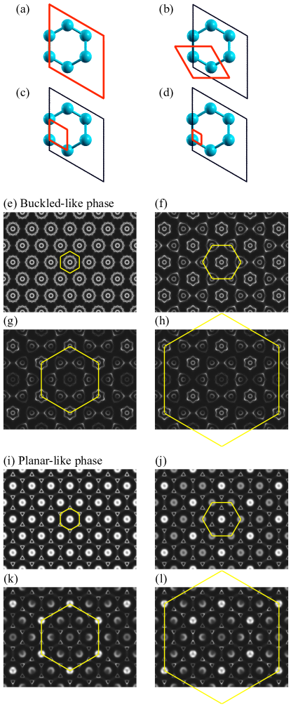
To illustrate the change of spectral weight associated with different conceptual unit cells, we first focus on isolated silicene sheets as thought to be peeled off from the optimized structures on the ZrB2 substrate. We emphasize that the conceptual unit cells could be smaller than the primitive () unit cell and the detailed description of conceptual unit cell can be found elsewhere.Ku et al. (2010); Lee et al. (2013b) The spectral weight on the constant-energy plane of 1.0 eV below are presented with different sizes of Brillouin zones sketched in Figs. 2 (a)-(d). For the () unit cell, a periodic pattern corresponding to a small Brillouin zone is obtained (Figs. 2 (e) and (i)). Once the unit cell is chosen as the () unit cell, shown in Fig. 2 (b), the spectral weight shows a different periodicity due to a higher degree of freedom (Figs. 2 (f) and (j)). This indicates that the translational symmetry breaking to () silicene leads to shadow bands and distributes the weight unevenly. In Fig. 2 (c), we further introduce an even smaller unit cell that contains a single Si atom. Then, the spectral weight is even more distributed (Figs. 2 (g) and (k)) as compared to the previous two cases. For example, the intensity at the zone center is reduced and some spectral weight disappears almost completely. However, when choosing even half of the lattice constant of that in Fig. 2 (c), the spectral weight is not altered, as shown in Figs. 2 (h) and (l), although the overall spectral weight is reduced by a factor of four. This is required to satisfy the sum rule. Note that once the unfolded spectral weight is folded into the smallest Brillouin zone related to the original () unit cell, the same spectral weight is exactly recovered.
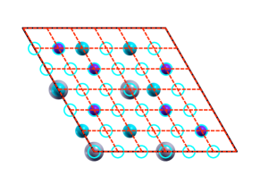
If the one-atom unit cell (Fig. 2 (c)) would be a reasonably good choice to allow for the presentation of translational symmetry breaking in a large BZ, the commensurability for a complicated system becomes an important issue. For silicene on ZrB2(0001), a good choice of the conceptual unit cell that contains only a single Si atom, a single Zr atom, and a single B atom for monolayer silicene and the topmost ZrB2 layer of the substrate, respectively, is shown by dashed lines in Fig. 3, as this is the largest commensurate one-atom unit cell. In the following, this unit cell is referred to as the “one-Si-atom unit cell”. In other words, the ()-reconstructed silicene can be reproduced upon removal of some ordered atoms, as vacancies, from the () supercell. As expected, the unfolded spectral weight reflects the strength of the symmetry breaking due to the vacancies and out-of-plane deviations of the atomic positions.
III.2 The calculated electronic band structure of silicene on ZrB2(0001)
Due to the epitaxial relationship to the Si(111) substrates, the experimentally observed in-plane lattice constant of ZrB2(0001) thin films is somewhat larger (3.187 Å) as compared to the experimentally observed (3.169 Å) and calculated (3.174 Å) Yamada-Takamura et al. (2010) bulk values. Even with this larger lattice constant, free-standing silicene prefers an in-plane lattice constant that is longer than that allowed by the epitaxial conditions imposed by the ZrB2(0001) surface.Lee et al. (2013a) Practically, as suggested by the observation of a regular arrangement of stripe domains in STM imagesFleurence et al. (2012) and by the relaxation of SiC atoms away from energetically unfavorable on-top positions as suggested by Si 2 core-level spectra,Friedlein et al. (2014) strain in silicene is released by structural relaxation accompanied by a small reduction of the areal density of Si atoms as compared to the system without stripe domains. While calculations that account for stripe domains require a huge supercell, a simpler way to simulate the reduction of the areal density is to explore larger in-plane lattice constants of the whole system. Additionally, the approximation for the exchange-correlation energy as used in the GGA is known to possibly overestimate the band width and could also give as much as up to 2% error in the lattice constants.Eastman et al. (1980); Haas et al. (2009); Yi et al. (2009) In the following, we therefore compare the results obtained for = 6.348 Å to those for the 2%-longer lattice constant of = 6.480 Å, where is the lattice constant of the () unit cell of the ZrB2(0001) reconstructed surface that corresponds to the () unit cell of silicene.
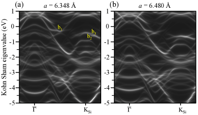
The electronic band structures represented in the BZ of the chosen commensurate conceptual one-Si-atom unit cell are shown in Figs. 4 and 5, for the buckled-like and planar-like phases, respectively. It should be mentioned that in this representation, the point is at high values of the in-plane component of the electron momentum, , while in the Figures, we indicate the () point of non-reconstructed silicene. Here, in order to allow a comparison with the intensity of ARPES spectra, each band is weighted by its spectral weight as derived from the imaginary part of the one-particle Kohn-Sham Green’s function.Ku et al. (2010); Lee et al. (2013b)
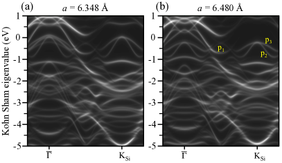
In this new representation, the differences between the band structures of buckled-like and planar-like epitaxial silicene phases are striking and substantial. Here, we focus on some of the most prominent and most conclusive features that are best recognized along the - direction. In particular, while for both phases, the top of the two upward curved features in the vicinity of at the point, shift down with increasing , in the case of the buckled-like phase, they form a flatter feature for = 6.480 Å but remain similar upward curved in the planar-like phase. The width of these bands, denoted and or and , for the buckled-like and planar-like phases, respectively, is reduced with which reflects the expansion of the bond length at the longer lattice constant. Note that these features bear some resemblance to the predicted Dirac cone of bands of free-standing, non-reconstructed silicene and are therefore of particular interest. A parabolic band is only present in the planar-like phase where its energy and dispersion is almost unaffected by the choice of . In contrast, the band of the buckled-like phase shows a v-like shape and the bottom weight is missing at = 6.480 Å. Many bands at higher binding energy are clearly similar for both phases, and are thus certainly be related to the bulk of the diboride substrate.
III.3 Comparison with ARPES spectra
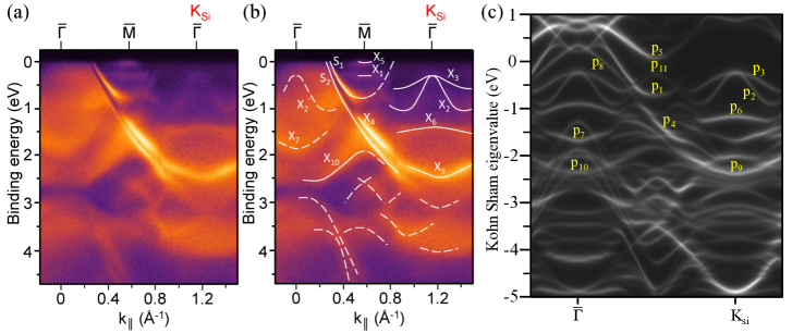
ARPES spectra obtained along the - direction and in a wide energy range, are shown in Figs. 6 (a) and (b). The spectra are similar to those reported previously for the low-binding energy region.Fleurence et al. (2012); Friedlein et al. (2013) Accordingly, we use the same notation to mark the individual features. While and have been assigned to diboride surface states,Fleurence et al. (2012) features - are related to the presence of silicene.Fleurence et al. (2012); Friedlein et al. (2013) Feature is mirrored as at thus following the symmetry of the ()-reconstructed silicene lattice. While has previously only been observed upon donation of electrons following the adsorption of potassium atoms,Friedlein et al. (2013) interestingly, in the present spectra, possibly due to the higher count rate caused by the increased flux of the undulator photon source, it can be recognized in the pristine sample. The bottom of the associated otherwise unoccupied band is therefore pinned at .
The comparison of the ARPES spectra with the band structure calculated for the planar-like phase at = 6.480 Å shows an astonishing and excellent quantitative agreement in terms of the energies and dispersions of electronic states. In particular, and clearly find their counterpart in and while the unoccupied band almost touches exactly halfway in between the and () points where feature is observed. The same good match is obtained between , , , , , , and and , , , , , and , respectively.
On the other hand, only partial agreement is found for the buckled-like phase, especially due to the lack of similarity between and . The band widths of and are also too narrow to compare with the experimental observations. The present results are therefore strong evidence that the structural properties of silicene on the ZrB2(0001) surface are very close to those of the planar-like phase that has been calculated to be the ground state stabilized by interactions between the Si honeycomb lattice and the metallic diboride surface.Lee et al. (2013a) In this context, it should again be emphasized that this could only be recognized now because of the implementation of two new methodological steps: (i) folding of bands is avoided by the choice of the one-Si-atom commensurate unit cell; and (ii) the exploration of larger in-plane lattice parameters.
The better agreement observed by enlarging may originate from the actual large lattice constant of the ZrB2 thin films or from the possibly reduced surface density of the Si atoms (which is reduced in order to avoid epitaxial strain) but it may also originate from the DFT calculation itself. We used GGA as an approximation for the exchange correlation energy in first-principles calculations. While the exact form of the exchange-correlation energy is unknown, it has been discussed that the approximations could give rise to a 2% error in the estimation of the lattice constantHaas et al. (2009) and to a bandwidth renormalization factor of 3 as compared to experiments.Yi et al. (2009) By enlarging the lattice constant, the Zr orbitals are effectively more localized. This in turn can give rise to a narrower band width as discussed before for approximations in the exchange-correlation energy.Eastman et al. (1980); Yi et al. (2009) Note that this could also cause a too small band gap. But even if the deviations in the exchange-correlation energy are accounted for, the agreement is quite remarkable since due to the presence of stress-related stripe domains, the real atomistic structure of silicene on the ZrB2(0001) surface is more complex than the one considered here.Fleurence et al. (2012)
III.4 The orbital character of the electronic states
Once settled that the band structure of DFT-proposed planar-like phase is consistent with the experimentally obtained ARPES data, the orbital character of the electronic states in this representation may be discussed. The individual contribution from Si , Si and Zr orbitals are shown in Figs. 7 (a), (b) and (c), respectively. All silicene-derived bands are hybridized to some extent with Zr electronic states, which is consistent with non-negligible interactions at the interface. In particular, while the upward curved bands and in the vicinity of the () point (that correspond to the spectral features and in the ARPES spectra) have major contributions from Si orbitals indeed, at the same time, they hybridize with the Si , , and the Zr orbitals. As already suggested in our previous work,Fleurence et al. (2012) these states are therefore of partial character. Importantly, the character is robust against the choice of the larger Brillouin zone. Bands and ( and ) also have strong contributions of orbitals and can be classified therefore as bands. On the other hand, bands and correspond to and in the ARPES spectra and have almost sole contributions from orbitals of the outermost Zr layer. This confirms that these states are diboride surface states indeed which survive upon the formation of the silicene layer, as has been concluded previously from experimental observations.Friedlein et al. (2013) Band () is a hybrid state with contributions from Si and Zr orbitals. Note that upon K atom adsorption, electrons are donated to and not to .Friedlein et al. (2013) This is consistent with the partial character of and sole electron donation to silicene-derived states.
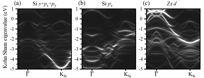
Our analysis shows that both bands and derive from combinations of the parabolic surface state of the pristine zirconium diboride surfaceLee et al. (2013a) with either Si or Si orbitals, for and , respectively. In other words, they are formed by rather non-local interactions between silicene and the substrate surface. On the other hand, if the SiC atoms are too close to Zr atoms, as they are in the buckled-like phase, local interactions destroy the diboride surface state.
Beside hybridization between silicene-derived and Zr-derived orbitals, we can recognize that there is also an apparent hybridization among Si , , and orbitals which reflects the intermediate hybridization of epitaxial silicene. Due to the complex hybridization, Si orbital contributions are spread out and occur up to binding energies of about 5 eV which is wider than the band width predicted for free-standing silicene of about 3-3.5 eV.Takeda and Shiraishi (1994); Cahangirov et al. (2009)
IV Conclusions
The combination of ARPES data obtained in a wide binding energy range, and the results of first-principles calculations allow for a yet unprecedented verification of the structural and electronic properties of epitaxial silicene on the ZrB2(0001) surface. In order to obtain best agreement with the experimental data and to avoid folding of bands, in the calculations, the small and commensurate conceptual unit cell containing a single Si atom, a single Zr atom and a single B atom (as well as Si, Zr and B vacancies) is chosen. Additionally, the in-plane lattice constant has been slightly increased in order likely to account for a misestimate of the exchange-correlation energy in the GGA and to simulate the effect caused by the larger lattice constant of ZrB2 thin films and the expected lower surface density of the Si atoms induced to avoid epitaxial strain.
Even if the actual stripe pattern observed in STM experimentsFleurence et al. (2012) is not accounted for, the excellent agreement between the experimental and calculated band structures are strong evidence that the structural properties of silicene on the ZrB2(0001) surface are very close to those of the planar-like phase. The results thus demonstrate that both calculations and experiment converge to this phase, which is stabilized by interactions between the Si honeycomb lattice and the metallic diboride surface.Lee et al. (2013a)
Finally, we have confirmed that all silicene-derived bands are hybridized to some extent with Zr electronic states, which is consistent with non-negligible interactions at the interface. But on the other hand, the zirconium diboride surface states survive upon the formation of silicene at the surface which indicates that these interactions are rather non-local. While the upward curved bands in the vicinity of the Fermi level at the () point are of partial character, they are hybridized with Si , , and Zr orbitals as well. This notable hybridization among Si , , and orbitals reflects the intermediate hybridization of epitaxial silicene.
Our new method of unfolding the band structures of the epitaxial layer and its substrate into a common conceptual unit cell enabled us to closely compare the electronic structures obtained theoretically and experimentally. The results therefore resolve the previously controversial issue related to the structural configuration of silicene on the ZrB2(0001) surface and its band structure. The method is anticipated to be a powerful tool for the study of the electronic structures of epitaxial two-dimensional materials in general.
Acknowledgements
We are grateful for experimental assistance from K. Mase (Institute of Materials Structure Science, KEK, Tsukuba, Japan), and for the use of the Cray XC30 machine at JAIST. The computational work was supported by the Strategic Programs for Innovative Research (SPIRE), MEXT, the Computational Materials Science Initiative (CMSI), and Materials Design through Computics: Complex Correlation and Non- Equilibrium Dynamics, A Grant in Aid for Scientific Research on Innovative Areas, MEXT, Japan. The experiments were performed under the approval of the Photon Factory Advisory Committee (Proposal No. 2012G610). YYT acknowledges financial support from the Funding Program for Next Generation World-Leading Researchers (GR046).
References
- Liu et al. (2011) C.-C. Liu, W. Feng, and Y. Yao, Phys. Rev. Lett. 107, 076802 (2011).
- Ezawa (2012a) M. Ezawa, Phys. Rev. Lett. 109, 055502 (2012a).
- Takeda and Shiraishi (1994) K. Takeda and K. Shiraishi, Phys. Rev. B 50, 14916 (1994).
- Cahangirov et al. (2009) S. Cahangirov, M. Topsakal, E. Aktürk, H. Şahin, and S. Ciraci, Phys. Rev. Lett. 102, 236804 (2009).
- Lee et al. (2013a) C.-C. Lee, A. Fleurence, R. Friedlein, Y. Yamada-Takamura, and T. Ozaki, Phys. Rev. B 88, 165404 (2013a).
- Ezawa (2012b) M. Ezawa, New J. Phys. 14, 033003 (2012b).
- Tsai et al. (2013) W.-F. Tsai, C.-Y. Huang, T.-R. Chang, H. Lin, H.-T. Jeng, and A. Bansil, Nature Commun. 4, 1500 (2013).
- Fleurence et al. (2012) A. Fleurence et al., Phys. Rev. Lett. 108, 245501 (2012).
- Wang and Ding (2013) Y. Wang and Y. Ding, Solid State Commun. 155, 6 (2013).
- Lin et al. (2012) C.-L. Lin et al., Appl. Phys. Express 5, 045802 (2012).
- Jamgotchian et al. (2012) H. Jamgotchian et al., J. Phys.: Condense. Matter 24, 172001 (2012).
- Vogt et al. (2012) P. Vogt et al., Phys. Rev. Lett. 108, 155501 (2012).
- Meng et al. (2013) L. Meng et al., Nano Lett. 13, 685 (2013).
- Chen et al. (2012) L. Chen et al., Phys. Rev. Lett. 109, 056804 (2012).
- Feng et al. (2012) B. Feng et al., Nano Lett. 12, 3507 (2012).
- Chiappe et al. (2012) D. Chiappe et al., Adv. Mater. 24, 5088 (2012).
- Chen et al. (2013) L. Chen, H. Li, B. Feng, Z. Ding, J. Qiu, P. Cheng, K. Wu, and S. Meng, Phys. Rev. Lett. 110, 085504 (2013).
- Avila et al. (2013) J. Avila et al., J. Phys.: Condens. Matter 25, 262001 (2013).
- Tsoutsou et al. (2013) D. Tsoutsou, E. Xenogiannopoulou, E. Golias, P. Tsipas, and A. Dimoulas, Appl. Phys. Lett. 103, 231604 (2013).
- Friedlein et al. (2013) R. Friedlein, A. Fleurence, J. T. Sadowski, and Y. Yamada-Takamura, Appl. Phys. Lett. 102, 221603 (2013).
- Fleurence et al. (2014) A. Fleurence et al., Appl. Phys. Lett. 104, 021605 (2014).
- Dietz and Eastman (1978) E. Dietz and D. E. Eastman, Phys. Rev. Lett. 41, 1674 (1978).
- Shirley et al. (1995) E. L. Shirley, L. J. Terminello, A. Santoni, and F. J. Himpsel, Phys. Rev. B 51, 13614 (1995).
- Zhou et al. (2006) S. Y. Zhou et al., Nature Phys. 2, 595 (2006).
- Bostwick et al. (2007) A. Bostwick et al., Nature Phys. 3, 36 (2007).
- Friedlein et al. (2014) R. Friedlein et al., J. Chem. Phys. 140, 184704 (2014).
- Ku et al. (2010) W. Ku, T. Berlijn, and C.-C. Lee, Phys. Rev. Lett. 104, 216401 (2010).
- Lee et al. (2013b) C.-C. Lee, Y. Yamada-Takamura, and T. Ozaki, J. Phys.: Condens. Matter 25, 345501 (2013b).
- Kohn and Sham (1965) W. Kohn and L. J. Sham, Phys. Rev. 140, A1133 (1965).
- Perdew et al. (1996) J. P. Perdew, K. Burke, and M. Ernzerhof, Phys. Rev. Lett. 77, 3865 (1996).
- Morrison et al. (1993) I. Morrison, D. Bylander, and L. Kleinman, Phys. Rev. B 47, 6728 (1993).
- Ozaki (2003) T. Ozaki, Phys. Rev. B 67, 155108 (2003).
- (33) T. Ozaki et al., http://www.openmx-square.org/.
- Ohwaki et al. (2012) T. Ohwaki, M. Otani, T. Ikeshoji, and T. Ozaki, J. Chem. Phys. 136, 134101 (2012).
- Kokalj (2003) A. Kokalj, Comp. Mater. Sci. 28, 155 (2003).
- Yamada-Takamura et al. (2010) Y. Yamada-Takamura, F. Bussolotti, A. Fleurence, S. Bera, and R. Friedlein, Appl. Phys. Lett. 97, 073109 (2010).
- Fleurence et al. (2013) A. Fleurence, W. Zhang, C. Hubault, and Y. Yamada-Takamura, Appl. Surf. Sci. 284, 432 (2013).
- (38) C.-H. Lin and W. Ku, http://arxiv.org/abs/1303.4822 (2013).
- Eastman et al. (1980) D. E. Eastman, F. J. Himpsel, and J. A. Knapp, Phys. Rev. Lett. 44, 95 (1980).
- Haas et al. (2009) P. Haas, F. Tran, and P. Blaha, Phys. Rev. B 79, 085104 (2009).
- Yi et al. (2009) M. Yi et al., Phys. Rev. B 80, 174510 (2009).