Highly reliable low-energy writing of bits in non-volatile multiferroic memory based on 180-degree magnetization switching with voltage-generated stress
Abstract
Rotating the magnetization of a magnetostrictive nanomagnet with electrically generated mechanical strain dissipates miniscule amount of energy compared to any other rotation method and would have been the ideal method to write bits in non-volatile magnetic memory, except strain cannot ordinarily rotate the magnetization of magnet by more than 90∘ and “flip” it. Here, we describe a scheme to achieve complete 180∘ rotation of the magnetization of a nanomagnet with strain that will enable writing of binary bits in non-volatile magnetic memory implemented with magneto-tunneling junctions whose soft layers are two-phase magnetostrictive/piezoelectric multiferroics. At room temperature, this writing method results in: (1) energy dissipation 6200 kT per bit, (2) write error probability 10-6, (3) write time of 1 ns, and (4) low read error. This could potentially lead to a new genre of non-volatile memory that is extremely reliable, fast and, at the same time, ultra-energy-efficient.
Magnetic random access memory (MRAM) is typically implemented with a magneto-tunneling junction (MTJ) comprising a hard and a soft ferromagnetic layer separated by a spacer that acts as a tunnel barrier. The soft layer is shaped like an elliptical disk that has two stable (mutually anti-parallel) magnetization states along its major axis. The hard layer is permanently magnetized parallel to one of those states. When the soft layer’s magnetization is parallel to that of the hard layer, the MTJ’s resistance is low and encodes one binary bit (say ‘0’), and when it is anti-parallel, the MTJ’s resistance is high and encodes the other bit (say ‘1’). Writing a bit involves orienting the magnetization of the soft layer either parallel or anti-parallel to that of the hard layer.
The oldest bit writing scheme used a magnetic field to flip the soft layer’s magnetization and that field was generated with an on-chip current. More recent schemes flip the magnetization with a spin transfer torque (STT) generated by passing a current through the MTJ Ralph and Stiles (2008), or domain wall motion induced by the current Yamanouchi et al. (2004), or by manipulating Rashba spin-orbit interaction at interfaces Miron et al. (2011). These schemes are extremely dissipative and result in dissipating 107 kT of energy per bit at room temperature Wang et al. (2013). A more energy-efficient scheme is to rotate the magnetization with a current utilizing the spin-Hall effect Liu et al. (2012) or spin-orbit torque in magnetically doped topological insulators Y.Fan et al. (2014), or use voltage-generated uniaxial strain/stress in a shape anisotropic magnetostrictive-piezoelectric (multiferroic) nanomagnet Atulasimha and Bandyopadhyay (2010); Roy et al. (2011); Fashami et al. (2011); Roy et al. (2013). The strain/stress is generated by applying an electrical voltage across the piezoelectric layer of the multiferroic nanomagnet which transfers the resulting strain to the magnetostrictive layer and rotates its magnetization.
Unfortunately, strain/stress can rotate the magnetization of a nanomagnet by only up to 90∘, which means that it is not able to “flip” the magnetization since that requires a 180∘ rotation. Once the stress is withdrawn, the magnetization, which has rotated by 90∘ and is now in an unstable state, will have roughly equal likelihood of returning to the original stable orientation (not flipping, or 0∘ rotation) or flipping to the other stable orientation (180∘ rotation). That makes the flipping only 50% likely, which is untenable. However, if the stress is withdrawn as soon as the magnetization vector has rotated by 90∘ from the original orientation, then a residual torque due to the magnetization vector’s out of plane component may continue to rotate it beyond 90∘ and achieve a “flip” with very high probability ( 99.99% at room temperature) Roy et al. (2013). Such precise withdrawal requires a feedback mechanism that determines when the magnetization has completed the 90∘ rotation and feeds that information back to the voltage generator to withdraw the stress at exactly the right juncture Roy et al. (2013). The need for such feedback circuitry makes this strategy unappealing since it introduces additional energy dissipation and complexity.
A clever idea to circumvent this problem is to apply a permanent magnetic field along the minor axis of the elliptical soft layer that dislodges the stable magnetization orientations from the major axis and places them along two axes that are in the plane of the magnet and mutually perpendicular. The hard layer of the MTJ is now magnetized parallel to one of these axes. If the soft layer has positive magnetostriction, then applying uniaxial tensile stress along one of these two axes brings the magnetization to the stable state along that axis, while applying compressive stress takes it to the other stable state (the situation is opposite if the magnetostriction coefficient is negative) Tiercelin et al. (2011); Giordano et al. (2012, 2013). Therefore, one type of stress (say, compressive) makes the hard and soft layer’s magnetization parallel and the other type (say, tensile) makes them mutually perpendicular. Thus, by choosing the sign of the stress, we can write either bit ‘0’ or bit ‘1’, regardless of the initially stored bit. The advantages are: 1) the stress withdrawal timing is not critical and no feedback mechanism is needed, 2) the final state is always stable; hence, the magnetization remains in the final state after the stress is withdrawn making the error probability very low ( 10-6 at room temperature), and 3) by choosing the sign of the stress (compressive or tensile), one can deterministically write either bit ‘0’ or bit ‘1’, without knowing what the initial stored bit was (i.e. there is no need to read the stored bit before re-writing it). On the flip side, the disadvantages are: 1) An external bias magnetic field is needed to dislodge the stable magnetization orientations from the ellipse’s major axis, and 2) the separation angle between the stable magnetization orientations is now which makes it harder to distinguish bit ‘1’ from bit ‘0’ when the latter are read via the resistance of the MTJ. The ratio of the MTJ resistances corresponding to bit ‘1’ and bit ‘0’ is when the magnetization of the hard layer is aligned along the stable direction representing the bit ‘0’ Bandyopadhyay and Cahay (2008). Here, and are the spin injection/detection efficiencies at the two ferromagnet/spacer interfaces of the MTJ. The resistance ratio is largest when and smaller when . In fact, if , then the resistance ratio is infinite when and only 2:1 when . Therefore, it is imperative to increase and bring it as close to 180∘ as possible. We were recently able to increase to 132∘ by applying stress (of the same sign) along two different directions (instead of applying compressive and tensile stress along the same direction) to write the two bits Biswas et al. (2014). However, this improves the resistance ratio only moderately.
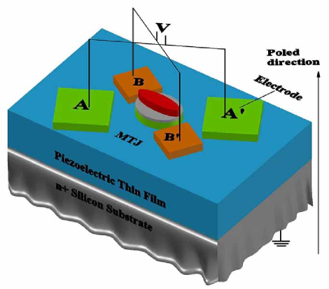
In this paper, we propose a scheme that can increase to 180∘ and also eliminates the bias magnetic field needed in Refs. [Tiercelin et al., 2011; Giordano et al., 2012, 2013; Biswas et al., 2014]. The only penalty we pay is that the write cycle must be preceded by a read cycle, i.e. we cannot deterministically write either bit ‘0’ or bit ‘1’ without first knowing what the initial stored bit was. Since reading is both faster than writing and dissipates far less energy, this penalty is minor. Figure 1(a) shows the schematic design of the memory element where the bit storing MTJ is placed on top of a piezoelectric Lead Zirconate Titanate (PZT) thin film deposited on an n+-Silicon substrate. The major axes of the elliptical hard and soft layers are collinear and the hard layer is permanently magnetized in one direction along its major axis. Two pairs of electrode pads are delineated on the PZT film such that the line joining one pair subtends an angle of 30∘ with the common major axis of the two layers and the other pair subtends an angle of 150∘. The magnetostrictive elliptical soft layer is in elastic contact with the PZT thin film and has a major axis = 110 nm, minor axis = 90 nm and thickness = 6 nm. These dimensions ensure that the soft nanomagnetic layer has a single domain Cowburn et al. (1999) and the in-plane potential energy barrier separating the stable magnetization orientations along its major axis is 62.5 kT at room temperature. The probability of spontaneous magnetization flipping between the two stable states due to thermal noise (static error probability) is therefore per attempt Brown (1963), leading to memory retention time years, assuming the attempt frequency is 1 THz Gaunt (1977).
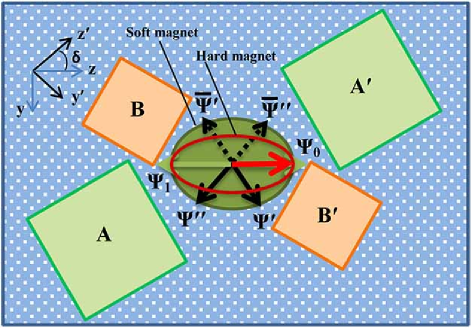
One pair of electrodes has edge dimension of 120 nm and the other has edge dimension of 80 nm whereas the thickness of the PZT thin film is 100 nm. These dimensions are needed to ensure the following: (1) the line joining the centers of each pair of pads subtends either 30∘ or 150∘ with the common major axis of the ellipses, (2) the spacing between the facing edges of the pads in either pair is comparable to the pads’ edge dimension and also the PZT film thickness, and (3) no two pads overlap. The hard layer of the MTJ is implemented with a synthetic anti-ferromagnet (SAF). When the magnetizations of the soft and hard layer are parallel (state in Figure 1(b)), the stored bit is ‘0’, and when they are anti-parallel (state ), the stored bit is ‘1’.
In order to write, say, bit ‘1’, we first read the resistance of the MTJ to determine what the stored bit is. If it is bit ‘1’, we do nothing. If it is bit ‘0’, then the magnetization of soft layer is at and we must switch it to (Figure 1(b)). To accomplish this, we apply a voltage between the electrode pair AA′ and the grounded n+-Silicon substrate.
Since the electrode in-plane dimensions are comparable to the piezoelectric film thickness, the out-of-plane () expansion/contraction and the in-plane () contraction/expansion of the piezoelectric regions underneath the electrodes produce a highly localized strain field under the electrodes Cui et al. (2013). Furthermore, since the electrodes are separated by a distance 1-2 times the PZT film thickness, the interaction between the local strain fields below the electrodes will lead to a biaxial strain in the PZT layer underneath the soft magnetic layer Cui et al. (2013). This biaxial strain (compression/tension along the line joining the electrodes and tension/compression along the perpendicular axis) is transferred to the soft magnetostrictive magnet by elastic coupling. If the magnetostriction coefficient of the latter is positive, then voltage of the correct polarity applied between AA′ and ground will generate compressive stress in the soft magnet, rotating its magnetization, while if the magnetostriction coefficient is negative, then voltage of the opposite polarity will cause the rotation. This rotation happens despite any substrate clamping and despite the fact that the electric field in the PZT layer just below the magnet is approximately zero since the metallic magnet shorts out the field Cui et al. (2013).
We will assume that the magnetostriction coefficient of the soft layer is positive and the applied voltage between AA′ and ground (of the right polarity) has generated compressive stress along the line AA′ and tensile stress in the direction perpendicular to this line. In that case, the magnetization will rotate away from towards . Once steady state is reached and the magnetization settles at some intermediate state which is roughly perpendicular to the axis joining the electrodes AA′, the voltage at AA′ is withdrawn (timing is not critical) and a voltage is applied between BB′ and the grounded substrate that will rotate the magnetization farther towards . Finally, upon reaching the new steady-state at which is roughly perpendicular to the line joining the electrode pair BB′, the voltage at BB′ is withdrawn (again, timing is not critical) and the magnetization vector will rotate spontaneously to the closer of the two global energy minima, which is . This results in flipping the magnetization and writing the desired bit ‘1’. Writing bit ‘0’, when the initial stored bit was ‘1’, is exactly equivalent and hence not discussed. Note that a two-phase clock is required to flip the bit – one phase tied to AA′ and the other to BB′.
In order to estimate the energy dissipated in writing the bit, the minimum time required to write, and the write error probability, we have carried out stochastic Landau-Lifshitz-Gilbert calculations in the manner of Ref. [Biswas et al., 2014]. For the sake of simplicity, we always consider uniaxial strain along the line joining the two electrodes of a pair, but the strain is actually biaxial resulting in tension/compression along that line and compression/tension along the perpendicular direction. The torques on the magnetization vector due to these two components add. Therefore, we underestimate the torque that makes the magnetization vector rotate, which makes all our dissipation, error probability and switching delay figures conservative.
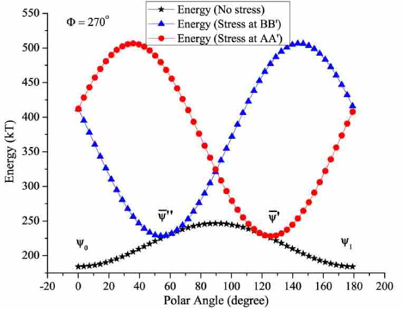
Figure 2 shows the potential energy profile of the nanomagnet in the magnet’s plane ( = 90∘, 270∘) as a function of the polar angle subtended by the magnetization vector with the common major axis of the elliptical hard and soft layers (z-axis). The three profiles correspond to the situations when neither electrode pair is activated, electrode pair AA′ is activated, and electrode pair BB′ is activated.
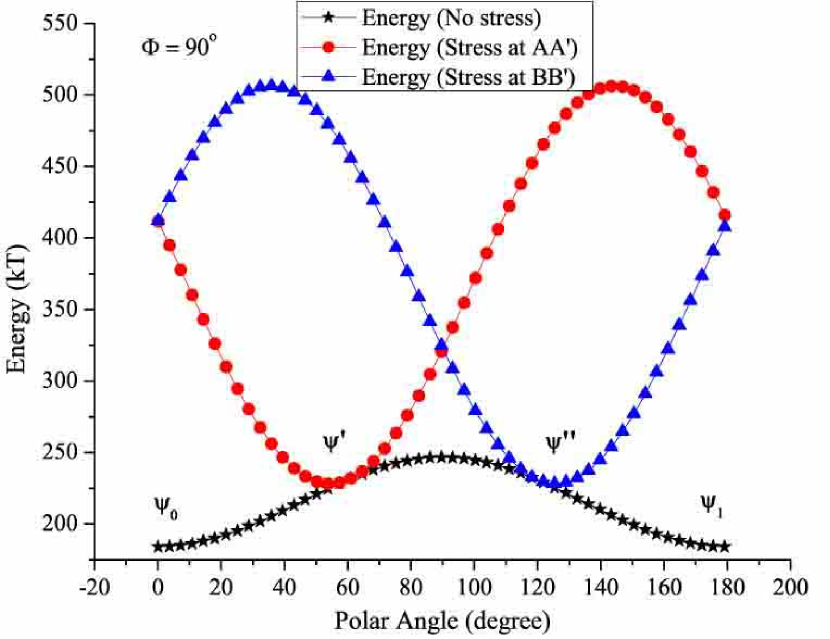
Consider the case when the magnetization of the nanomagnet is initially in the stable state (initial stored bit is ‘0’). If the electrode pair AA′ is activated, a compressive uniaxial stress component is generated along the line joining that electrode pair, which will rotate the magnetization vector to since that corresponds to the only accessible global energy minimum (see the energy profile corresponding to in Fig. 2). The other global minimum at is inaccessible owing to the energy barrier between and (see energy profile corresponding to in Fig. 2; the peak of the energy barrier separating and is located roughly at ). In other words, the magnetization will rotate clockwise instead of anti-clockwise in Fig. 1(b). Next, de-activating AA′ and activating BB′ causes a uniaxial compressive stress component along the line joining BB′ that will rotate the magnetization clockwise to the new global energy minimum , which is the only accessible one. Finally, removal of stress will drive the magnetization to (writing the new bit ‘1’) since it is the only accessible global energy minimum at that point. The other global energy minimum at is inaccessible because of the energy barrier between and . The height of this energy barrier 20 kT which prevents the magnetization from migrating to as opposed to .
If we activate the electrode pairs in opposite sequence, i.e. BB′ first and then AA′, the magnetization will first rotate anti-clockwise from to , then anti-clockwise to and finally anti-clockwise to (see the energy profile corresponding to ). Therefore, the sequence does not matter; activating the electrodes in either sequence always flips the bit - either by clockwise rotation or anti-clockwise rotation depending on the sequence. It is easy to verify that the same is true if the initial stored bit was ‘1’ instead of ‘0’.
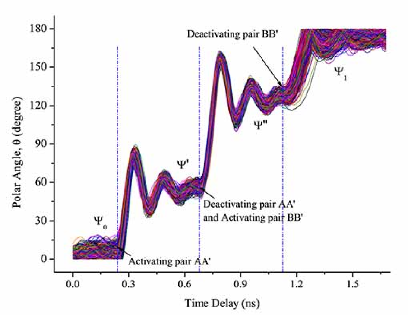
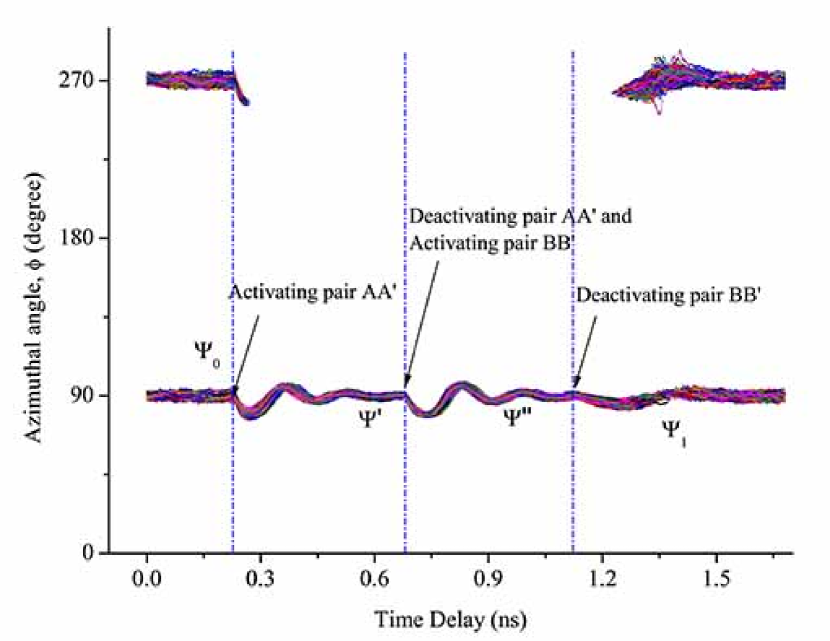
In Fig. 3, we show 1,000 randomly chosen switching trajectories (magnetization orientation versus time) out of 106 trajectories simulated in the presence of room temperature thermal noise. These switching trajectories are generated from stochastic Landau-Lifshitz-Gilbert simulations in the manner of ref. [Biswas et al., 2014]. The initial values of and are chosen from their thermal distributions around with appropriate weight Biswas et al. (2014), the fluctuation of the magnetization around the initial orientation is simulated for 2.3 ns and then the pair AA′ is activated (stress is turned on). The intermediate steady state () is reached by all 106 trajectories within 0.45 ns after activation, at which point AA′ is deactivated and BB′ is activated. The next intermediate steady state () is reached by all trajectories within another 0.45 ns, and then BB′ is deactivated (stress is turned off). The simulation of the trajectories is continued until for every one of 106 trajectories, reaches within 4∘ of 180∘ (successful flip). This takes another 0.46 ns. The trajectories in Fig. 3 are all slightly different from each other since they are probabilistic in the presence of room temperature thermal noise. One million trajectories were simulated and all of them showed successful transition from to , implying that the switching failure probability is . Therefore, the minimum switching delay for error probability is 0.45 + 0.45 + 0.46 ns = 1.36 ns. This is the minimum time needed for all 106 switching trajectories to complete flipping.
It is obvious that the present scheme has the shortcoming that it will erroneously write the wrong bit every time the stored bit happens to be the desired bit (since the stored bit is always flipped in the write step). Therefore, a write cycle must be preceded by a read cycle to determine the stored bit. If the stored bit is the same as the desired bit, no action is taken. Otherwise, the bit is flipped following the above procedure. This requires an extra read cycle, but it also saves time and energy by obviating the write cycle whenever the stored and desired bits are the same. Since writing is both slower and more dissipative than reading, there may be an overall gain.
The write error probability can be reduced to zero by writing the bit, then reading it to verify if it was written correctly, re-writing it if it was written incorrectly, followed by another read and so on, until the bit is verified to have been written correctly. Alternately, we can always carry out a fixed number of write/verification cycles. The error probability after such cycles is since it is the probability of having written the bit incorrectly times in a row. Because it will be an overkill to reduce the write error probability to below the static error probability of , just four ( = 4) read/verification cycles will be sufficient. However, this increases the write time. Even if the bit was written correctly in the first attempt, we will still need three additional idle cycles since all bits are written simultaneously in parallel. This will increase the effective write time to 1.364 ns = 5.44 ns (again assuming that the read time is negligible compared to the write time), resulting in a clock rate of 180 MHz.
The results in Fig. 3 were generated assuming the following material parameters for the magnet (Terfenol-D): saturation magnetization A/m, magnetostriction coefficient , Young’s modulus = 80 GPa, and Gilbert damping coefficient Abbundi and Clark (1977); Ried et al. (1998); Kellogg and Flatau (2008). We also assume: strain (stress = 30 MPa).
In ref. [Cui et al., 2013], the electric field needed to generate a local strain of 10-3 in the magnet was 3 MV/m. Using a linear interpolation, the electric field needed to generate a strain of would be 1.125 MV/m. Therefore, the potential that needs to be applied to the electrodes is 1.125 MV/m 100 nm = 112.5 mV.
The energy dissipated in writing the bit has two components: (1) the internal dissipation in the nanomagnet due to Gilbert damping, which is calculated in the manner of Ref. [Roy et al., 2012] for each trajectory (the mean dissipation is the dissipation averaged over all trajectories that result in correct switching); and (2) the external (1/2) dissipation associated with applying the voltage between the electrodes and the grounded substrate which act as a capacitor. Since the piezoelectric response of PZT is much faster than the magnet switching Li et al. (2004), we can view the strain generation as instantaneous.
The larger electrodes have a lateral dimension of 120 nm and the PZT film thickness is 100 nm. Therefore, the associated capacitance is = 1.275 fF, if we assume that the relative dielectric constant of PZT is 1000. Since the two electrodes of a pair are always activated together, the external energy dissipation will be twice (1/2) dissipation and that value is 3896 kT at room temperature ( = 112.5 mV). The smaller electrode pair has a lateral dimension of 80 nm and hence a smaller capacitance of 0.567 fF. Hence, it dissipates energy of 1733 kT. The mean internal dissipation could depend on whether the initial stored bit was ‘0’ or ‘1’, and we will take the higher value. In this case, the higher value was 514 kT, thus making the total dissipation 6143 kT which is at least two orders of magnitude less than what spin-transfer-torque memory STT-RAM dissipates in a write cycle Wang et al. (2013).
In conclusion, we have provided a straintronic bit writing scheme that results in low energy dissipation, low write and read error rate, and fast writing speed. The only disadvantage is that every write cycle must be preceded by a read cycle, but it is a minor penalty.
This work was supported by the US National Science Foundation under grants ECCS-1124714 and CCF-1216614. J. A. would also like to acknowledge the NSF CAREER grant CCF-1253370.
References
- Ralph and Stiles (2008) Ralph, D. C.; Stiles, M. D. Spin transfer torques. J. Magn. Magn. Mater. 2008, 320, 1190–1216.
- Yamanouchi et al. (2004) Yamanouchi, M.; Chiba, D.; Matsukura, F.; Ohno, H. Current-induced domain-wall switching in a ferromagnetic semiconductor structure. Nature 2004, 428, 539–542.
- Miron et al. (2011) Miron, I. M.; Garello, K.; Gaudin, G.; Zermatten, P.-J.; Costache, M. V.; Auffret, S.; Bandiera, S.; Rodmacq, B.; Schuhl, A.; Gambardella, P. Perpendicular switching of a single ferromagnetic layer induced by in-plane current injection. Nature 2011, 476, 189–193.
- Wang et al. (2013) Wang, K. L.; Alzate, J. G.; Amiri, P. K. Electric-field-induced thermally assisted switching of monodomain magnetic bits. J. Phys. D: Appl. Phys. 2013, 46, 074003.
- Liu et al. (2012) Liu, L.; Pai, C.-F.; Li, Y.; Tseng, H. W.; Ralph, D. C.; Buhrman, R. A. Spin-torque switching with the giant spin Hall effect of Tantalum. Science 2012, 336, 555–558.
- Y.Fan et al. (2014) Y.Fan,; Upadhyaya, P.; Kou, X.; Lang, M.; Takei, S.; Wang, Z.; Tang, J.; He, L.; Chang, L.-T.; Montazeri, M. et al. Magnetization switching through giant spin orbit torque in a magnetically doped topological insulator heterostructure. Nature Mater. 2014, 13, 699–704.
- Atulasimha and Bandyopadhyay (2010) Atulasimha, J.; Bandyopadhyay, S. Bennett clocking of nanomagnetic logic using multiferroic single-domain nanomagnets. Appl. Phys. Lett. 2010, 97, 173105.
- Roy et al. (2011) Roy, K.; Bandyopadhyay, S.; Atulasimha, J. Hybrid spintronics and straintronics: A magnetic technology for ultra low energy computing and signal processing. Appl. Phys. Lett. 2011, 99, 063108.
- Fashami et al. (2011) Fashami, M. S.; Roy, K.; Atulasimha, J.; Bandyopadhyay, S. Magnetization dynamics, throughput and energy dissipation in a universal multiferroic nanomagnetic logic gate with fan-in and fan-out. Nanotechnology 2011, 22, 155201.
- Roy et al. (2013) Roy, K.; Bandyopadhyay, S.; Atulasimha, J. Binary switching in a ‘symmetric’ potential landscape. Sci. Reports 2013, 03, 3038.
- Tiercelin et al. (2011) Tiercelin, N.; Dusch, Y.; Preobrazhensky, V.; Pernod, P. Magnetoelectric memory using orthogonal magnetization states and magnetoelastic switching. J. Appl. Phys. 2011, 109, 07D726.
- Giordano et al. (2012) Giordano, S.; Dusch, Y.; Tiercelin, N.; Pernod, P.; Preobrazhensky, V. Combined nanomechanical and nanomagnetic analysis of magnetoelectric memories. Phys. Rev. B 2012, 85, 155321.
- Giordano et al. (2013) Giordano, S.; Dusch, Y.; Tiercelin, N.; Pernod, P.; Preobrazhensky, V. Thermal effects in magnetoelectric memories with stress-mediated switching. J. Phys. D: Appl. Phys. 2013, 46, 325002.
- Bandyopadhyay and Cahay (2008) Bandyopadhyay, S.; Cahay, M. Introduction to Spintronics; CRC Press: Boca Raton, 2008.
- Biswas et al. (2014) Biswas, A. K.; Bandyopadhyay, S.; Atulasimha, J. Energy-efficient magnetoelastic non-volatile memory. Appl. Phys. Lett. 2014, 104, 232403.
- Cowburn et al. (1999) Cowburn, R. P.; Koltsov, D. K.; Adeyeye, A. O.; Welland, M. E.; M.Tricker, D. Single-domain circular nanomagnets. Phys. Rev. Lett. 1999, 83, 1042–1045.
- Brown (1963) Brown, W. F., Jr. Thermal fluctuations of a single-domain particle. Phys. Rev. 1963, 130, 1677–1686.
- Gaunt (1977) Gaunt, P. The frequency constant for thermal activitation of a ferromagnetic domain wall. J. Appl. Phys. 1977, 48, 3470–3474.
- Cui et al. (2013) Cui, J.; Hockel, J. L.; Nordeen, P. K.; Pisani, D. M.; Liang, C.; Carman, G. P.; Lynch, C. S. A method to control magnetism in individual strain-mediated magnetoelectric islands. Appl. Phys. Lett. 2013, 103, 232905.
- Abbundi and Clark (1977) Abbundi, R.; Clark, A. E. Anomalous thermal expansion and magnetostriction of single crystal TbDyFe2. IEEE Trans. Magn. 1977, 13, 1519–1520.
- Ried et al. (1998) Ried, K.; Schnell, M.; Schatz, F.; Hirscher, M.; Ludescher, B.; Sigle, W.; Kronmüller, H. Crystallization behaviour and magnetic properties of magnetostrictive TbDyFe films. Phys. Status Solidi A 1998, 167, 195–208.
- Kellogg and Flatau (2008) Kellogg, R.; Flatau, A. Experimental investigation of Terfenol-D’s elastic modulus. J. Intell. Mater. Syst. Struct. 2008, 19, 583–595.
- Roy et al. (2012) Roy, K.; Bandyopadhyay, S.; Atulasimha, J. Energy dissipation and switching delay in stress-induced switching of multiferroic nanomagnets in the presence of thermal fluctuations. J. Appl. Phys. 2012, 112, 023914.
- Li et al. (2004) Li, J.; Nagaraj, B.; Liang, H.; Cao, W.; Lee, C. H.; Ramesh, R. Ultrafast polarization switching in thin-film ferroelectrics. Appl. Phys. Lett. 2004, 84, 1174–1176.