A Strained Silicon Cold Electron Bolometer using Schottky Contacts
Abstract
We describe optical characterisation of a Strained Silicon Cold Electron Bolometer (CEB), operating on a stage, designed for absorption of millimetre-wave radiation. The silicon Cold Electron Bolometer utilises Schottky contacts between a superconductor and an n++ doped silicon island to detect changes in the temperature of the charge carriers in the silicon, due to variations in absorbed radiation. By using strained silicon as the absorber, we decrease the electron-phonon coupling in the device and increase the responsivity to incoming power. The strained silicon absorber is coupled to a planar aluminium twin-slot antenna designed to couple to and that serves as the superconducting contacts. From the measured optical responsivity and spectral response, we calculate a maximum optical efficiency of for radiation coupled into the device by the planar antenna and an overall noise equivalent power (NEP), referred to absorbed optical power, of when the detector is observing a source through a throughput limiting aperture. Even though this optical system is not optimised we measure a system noise equivalent temperature difference (NETD) of . We measure the noise of the device using a cross-correlation of time stream data measured simultaneously with two junction field-effect transistor (JFET) amplifiers, with a base correlated noise level of and find that the total noise is consistent with a combination of photon noise, current shot noise and electron-phonon thermal noise.
I Introduction
Photon noise limited detection of millimetre-wave radiation has been demonstrated with a number of cryogenic detectors such as: semiconductor bolometers, transition edge sensors and kinetic inductance detectorsMorozov et al. (2011); Doyle et al. (2008). A bolometer consists of a thermally isolated absorber that converts absorbed radiation into thermal energy, which is detected by means of a sensitive thermometer. The concept of using the weak coupling between electrons and phonons at low temperatures, combined with a normal metal-insulator-superconductor (NIS) tunnel junction thermometer, to make a fast and sensitive hot electron bolometer was first proposed by Nahum, Richards and MearsNahum, Richards, and Mears (1993); Nahum, Eiles, and Martinis (1994). Dual normal metal-insulator-superconductor (SINIS) junctions, coupled to an absorbing metallic island, can be used to simultaneously act as a microrefrigerator by extracting heat from the electrons and as a bolometric detector. The wavelengths that the island absorbs can be defined by patterning the superconducting leads into an antenna.
Schmidt et al.Schmidt et al. (2005) describe how the use of a combined microwave and DC biasing signal, along with frequency domain multiplexing techniques, can be used to realise large imaging arrays (up to pixels) of cold electron bolometers.
Detailed calculations of the characteristics of these Cold Electron Bolometers (CEBs) indicate that they should exhibit a combination of fast response speeds () and high sensitivity. Achieving high sensitivities with metal-based Cold Electron Bolometers requires fabrication of submicron metal islands.
Replacing the normal metal with a degenerately doped silicon offers reduced electron-phonon coupling compared to standard metals and thus gives higher sensitivity for a given island volumeLeoni (1999). It has been proposedMuhonen et al. (2011) that using a strained silicon absorber enables fabrication of detectors with photon noise limiting sensitivity using standard photolithographic techniques. Initial reports of optical noise equivalent power for metal based Cold Electron Bolometers have been published in recent yearsOtto et al. (2013); Tarasov et al. (2011). Most of these measurements have been based on radiation absorbed from a cold blackbody source, this does not allow for the spectral response of the detector to be studied. They have also all reported optical noise equivalent powers limited by the readout electronics. Here we present optical measurements of a Strained Silicon Cold Electron Bolometer designed to absorb millimetre-wave radiation, these measurement have been taken with the detector looking out of a window in the cryostat which allowed for a number of sources, including a Fourier transform spectrometer, to be observed.
II Theory
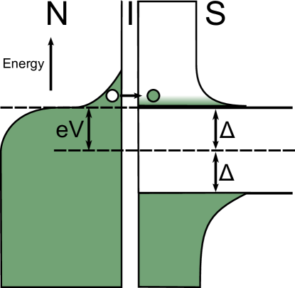
The electrothermal properties of both the normal metal-insulator-superconductor and the symmetric (SINIS) structure have been well studied Pekola (2005); Nahum, Richards, and Mears (1993); Nahum, Eiles, and Martinis (1994); Leivo, Pekola, and Averin (1996); Savin et al. (2001); Pekola et al. (2004). FIG. 1 shows a typical normal metal-insulator-superconductor structure (shown in the presence of an external bias such that ). These devices have been shownPekola et al. (2004) to be able to reduce electron temperature from to below . For a sensitive bolometric detector we would like the absorber (the normal metal in this case) to have as small a volume as possible.
A similar structure, superconductor-semiconductor-superconductor (SSmS), exists where the normal metal is replaced by a doped semiconductor and the insulator replaced by a Schottky contact formed between the semiconductor and the superconductorSavin et al. (2001). These devices have the advantage of decreased electron-phonon coupling compared to the normal metal based type of deviceMuhonen et al. (2011) and reduced electron density. The current, , flowing through each of the symmetric junctions is given by:
| (1) |
where is the normal-state resistance due to tunnelling through the insulating barrier, is half the superconducting bandgap, is the voltage across the structure and is the Fermi distribution for electrons at temperature . Associated with this current is a flow of heat from the central island which dissipates a power, , within the device of:
| (2) |
This power is bias dependent and is negative (cooling) for bias voltages .
In a Cold Electron Bolometer when the absorber is heated by incident optical power it is this cooling power, associated with the most energetic of charges tunnelling out of the absorber, which removes the heat. Since the cooling (thermal resetting) of the bolometer is carried out directly by electron diffusion (as opposed to the long, weak, thermal links required by many of today’s most sensitive bolometers Mauskopf et al. (1997); Audley et al. (2012); Holland et al. (2013)) the thermal time constant associated with the Cold Electron Bolometer is governed by the tunnelling time. This can be Kuzmin (2004) as low as , whereas other types of detector Jackson et al. (2012) have response times of the order of .
In addition to this cooling power, the electrons are also heated or cooled by the weak thermal link to the phonons. This heating term, , is given by:
| (3) | ||||
| where is a material constant that has been measuredPrest et al. (2011) to be ; is the volume of the bolometer’s absorber; and are the phonon and electron temperatures respectively and the power has been foundPrest et al. (2011) to be . From this we can define a thermal conductance, , from the phonons to the electrons as: | ||||
| (4) | ||||
The total noise equivalent power (NEP) for the Cold Electron Bolometer is comprised of several terms and has been fully derived by Golubev and Kuzmin (2001)Golubev and Kuzmin (2001) to be:
| (5) |
where is the noise of the readout amplifier and is the responsivity of the detector, which is a function of bias, is the heat flow noise and is the current noise. The use of strained silicon reduces the constant by a factor of compared to unstrained siliconPrest et al. (2011), this results in a corresponding improvement in the second term of EQN. 5 (the phonon noise).
The other dominant limiting factor to the noise equivalent power will be due to the absorption of photons into the strained silicon. This photon noise term is:
| (6) |
where and are the frequency and power of the incident radiation respectively and is the optical bandwidth.
III Device Design
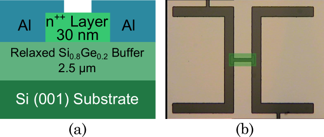
One advantage of the silicon based Cold Electron Bolometer compared to those utilising a metal absorber (SINIS) is that since the tunnel barrier is formed by a Schottky contact the is no need to fabricate separate insulating layers. The Strained Silicon Cold Electron Bolometer, studied in this work, consists of three elements: Firstly, the silicon substrate has an epitaxially grown thick relaxed SiGe (80 % silicon) straining layer. On top of the straining layer is a thick layer of n++ doped silicon () etched to form a rectangular mesa with an area of . Finally the top layer is a thick film of e-beam evaporated aluminium. This final layer is patterned to form both the contacts to the doped silicon absorber and a twin slot antenna. The contacts to the absorber are both and have a give a tunnelling resistance of . The twin slot antenna has been designed to couple radiation to the central absorber and the coupling has been simulated with Ansoft’s HFSS software prior to fabrication. The device design is shown in FIG. 2.
IV Experimental Procedure
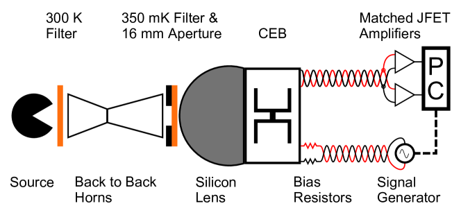
A schematic of the testing setup is shown in FIG. 3. The detector was housed in a liquid helium cryostat and cooled to using a helium-3 refrigerator. Radiation, visible through a window in the outer cryostat shield, was fed in to a pair of back-to-back horns, the beam from this horn pair was then focussed on to the detector’s antenna by a hemispherical silicon lens. This optical coupling scheme was not optimised for high efficiency but designed to minimise stray light coupling to the device.
The detector was current biased using a differential voltage source and a pair of cold biasing resistors. The voltage output of the detector was fed into two matched JFET differential amplifiers, each of which had an input referred noise of . The output of each of these amplifiers was then passed to a computer which cross-correlated the signal in real time and resulted in a final input referred correlated noise, after averaging, of for the readout system. For optical testing we used an eccosorb load chopped between and .
V Results
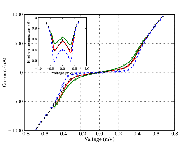
The Silicon Cold Electron Bolometer has been tested both dark and optically loaded. Dark measurements consist of current-voltage (IV) characterisation at various bath (phonon) temperatures. The optical response of the device to a variable temperature blackbody source has also been measured. FIG. 4 compares the current-voltage relationship for the detector in these various conditions; it can be seen that the optically loaded measurements correspond to higher electron temperature in the device and therefore more linear current-voltage curves compared to the corresponding unloaded measurement. In fact the optically loaded curves are similar to a dark measurement at a much higher phonon temperature.
From the measured voltage for a given current bias and using EQN. 1 we can calculate the temperature of the electrons. This model, shown as the lines in FIG. 4, shows that a high quality fit to the data (open circles) can be achieved based on this algorithm in all cases. The electron temperatures found from this fit were and at zero bias for the and illuminations. The increase from the phonon temperature of is accounted for by the incident power heating the electrons. At a bias corresponding to a voltage of across the detector, the minimum electron temperatures achieved for the two illumination levels were and . By use of EQN. 3 at zero bias, combined with the dimensions of the absorbing island and the measured value of and assuming the electron temperature is significantly greater than that of the phonons, we compute the absorbed power to be & for the two load temperatures. We believe there is a contribution of approximately from stray light to both of these powers.
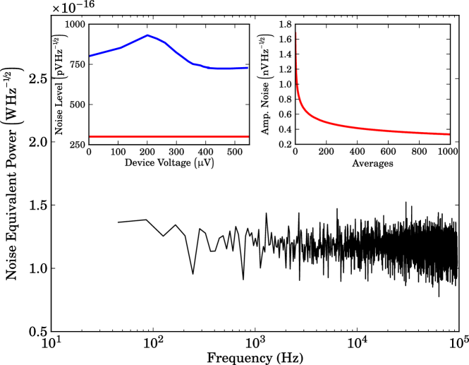
The responsivity, at a particular current bias, of the Cold Electron Bolometer can be calculated from the change in the voltage when the incident power changes by a known amount. From the calculated absorbed powers for the two illuminations and the voltage changes resulting from this change (seen in FIG. 4), we calculate the responsivity to have a maximum of for the source and for the room temperature source. In both cases the maximum responsivity occurs when the voltage across the device is just below , as is expected. FIG. 5 shows the noise equivalent power calculated from these results. For both the & the loading this is dominated by photon noise. From FIG. 5 we see that the noise equivalent power is .
The speed of the detector can be found from the roll-off in the white noise level from the photon noise or from measuring the change in responsivity for a modulated signal as a function of frequency. We attempted to measure this using a coherent tunable source which could be chopped on and off at frequencies up to 6 kHz but did not see any reduction in the signal and we also did not see any roll-off in the noise power (as seen in FIG. 5) up to the bandwidth of the readout amplifier . From this, we conclude that the time-constant of this detector is less than .
From EQN. 5 we compute that the limit on the electrical (dark) noise equivalent power, for optical loading less than , from the electron-phonon interaction is , this compares well to the ‘dark’ noise equivalent power estimations for hot electron bolometer type devices operating at comparable phonon temperaturesKarasik and Cantor (2011), which share a common noise limit in these circumstances. The current proof of concept detector has a very large absorbing element, if this was reduced by a factor of (which is still larger than the absorbing element of the comparable hot electron bolometerKarasik and Cantor (2011) and still possible with standard photolithography) the phonon noise limit would be reduced to for the same operating temperature.
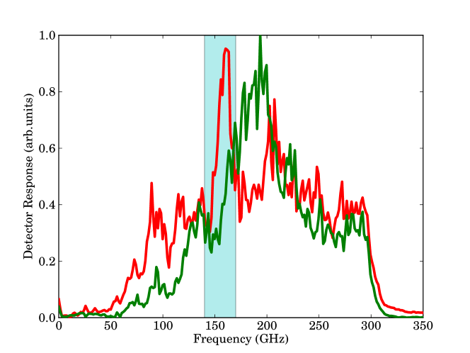
We have also measured the response of the Strained Silicon Cold Electron Bolometer as a function of the frequency of incident radiation. This was performed in both linear polarisations; since the detector used a twin-slot antenna to couple radiation it was expected that there would be more response in one polarisation. The measured spectral response is shown in FIG. 6. The measured response has a cutoff of due to the optical filters in place. The highlighted region denotes the expected frequency range of the twin-slot antenna. There is a clear excess response in this region in the vertical polarisation, parallel to the twin slot antenna. The peak in the horizontal polarisation may be attributed to response in the coplanar waveguide (CPW), which couples radiation to the absorber and is also due to the cuts in the aluminium (seen in FIG. 2b), which break the DC continuity around the detector. Both these cuts and the coplanar waveguide are orthogonal to the twin-slot antenna. The plateau level, around half of the maximum response, is due to a combination of photons directly splitting Cooper pairs in the aluminium along with direct absorption in the doped silicon mesa, general broadening of the absorption spectrum due to the silicon lens and the integrating cavity in which the detector was housed.
VI Conclusion
We have demonstrated a detector that utilises direct electron cooling via Schottky tunnelling contacts between aluminium and strained silicon. We have shown that this detector has a photon noise limited noise equivalent power of when observing a blackbody and under low optical loading conditions has an electrical or dark noise equivalent power, at , of . The time constant of this detector has been determined to be less than , which compares extremely favourably to other detector types with similar noise equivalent power.
This work has been financially supported by the EPSRC through grant numbers EP/F040784/1 and EP/J001074/1, and by the Academy of Finland through grant number 252598.
References
- Morozov et al. (2011) D. Morozov, P. Mauskopf, P. Ade, M. Ridder, P. Khosropanah, M. Bruijn, J. Van der Kuur, H. Hoevers, J. Gao, and D. Griffin, Applied Superconductivity, IEEE Transactions on 21, 188 (2011).
- Doyle et al. (2008) S. Doyle, P. Mauskopf, J. Naylon, A. Porch, and C. Duncombe, Journal of Low Temperature Physics 151, 530 (2008).
- Nahum, Richards, and Mears (1993) M. Nahum, P. Richards, and C. Mears, Applied Superconductivity, IEEE Transactions on 3, 2124 (1993).
- Nahum, Eiles, and Martinis (1994) M. Nahum, T. M. Eiles, and J. M. Martinis, Applied Physics Letters 65, 3123 (1994).
- Schmidt et al. (2005) D. R. Schmidt, K. W. Lehnert, A. M. Clark, W. D. Duncan, K. D. Irwin, N. Miller, and J. N. Ullom, Applied Physics Letters 86 (2005).
- Leoni (1999) R. Leoni, New Astronomy Reviews 43, 317 (1999).
- Muhonen et al. (2011) J. T. Muhonen, M. J. Prest, M. Prunnila, D. Gunnarsson, V. A. Shah, A. Dobbie, M. Myronov, R. J. H. Morris, T. E. Whall, E. H. C. Parker, and D. R. Leadley, Applied Physics Letters 98 (2011).
- Otto et al. (2013) E. Otto, M. Tarasov, P. K. Grimes, A. Chekushkin, L. S. Kuzmin, and G. Yassin, Superconductor Science and Technology 26, 085020 (2013).
- Tarasov et al. (2011) M. Tarasov, L. Kuzmin, V. Edelman, S. Mahashabde, and P. De Bernardis, Applied Superconductivity, IEEE Transactions on 21, 3635 (2011).
- Pekola (2005) J. Pekola, Nature 435, 289 (2005).
- Leivo, Pekola, and Averin (1996) M. M. Leivo, J. P. Pekola, and D. V. Averin, Applied Physics Letters 68, 1996 (1996).
- Savin et al. (2001) A. M. Savin, M. Prunnila, P. P. Kivinen, J. P. Pekola, J. Ahopelto, and A. J. Manninen, Applied Physics Letters 79, 1471 (2001).
- Pekola et al. (2004) J. P. Pekola, T. T. Heikkilä, A. M. Savin, J. T. Flyktman, F. Giazotto, and F. W. J. Hekking, Phys. Rev. Lett. 92, 056804 (2004).
- Mauskopf et al. (1997) P. D. Mauskopf, J. J. Bock, H. D. Castillo, W. L. Holzapfel, and A. E. Lange, Appl. Opt. 36, 765 (1997).
- Audley et al. (2012) M. D. Audley, G. de Lange, J.-R. Gao, P. Khosropanah, M. Ridder, L. Ferrari, W. M. Laauwen, M. Ranjan, P. D. Mauskopf, D. Morozov, and N. A. Trappe, in Proc. SPIE 8452 (2012) pp. 84520B–84520B–12.
- Holland et al. (2013) W. S. Holland, D. Bintley, E. L. Chapin, and A. Chrysostomou, Monthly Notices of the Royal Astronomical Society 430, 2513 (2013).
- Kuzmin (2004) L. Kuzmin, in 12th International Conference on Infrared and Millimeter Waves (2004) pp. 239–240.
- Jackson et al. (2012) B. D. Jackson, P. A. J. De Korte, J. Van der Kuur, P. Mauskopf, J. Beyer, M. Bruijn, A. Cros, J. Gao, D. Griffin, R. Den Hartog, M. Kiviranta, G. De Lange, B. van Leeuwen, C. Macculi, L. Ravera, N. Trappe, H. Van Weers, and S. Withington, Terahertz Science and Technology, IEEE Transactions on 2, 12 (2012).
- Prest et al. (2011) M. J. Prest, J. T. Muhonen, M. Prunnila, D. Gunnarsson, V. A. Shah, J. S. Richardson-Bullock, A. Dobbie, M. Myronov, R. J. H. Morris, T. E. Whall, E. H. C. Parker, and D. R. Leadley, Applied Physics Letters 99, 251908 (2011).
- Golubev and Kuzmin (2001) D. Golubev and L. Kuzmin, Journal of Applied Physics 89, 6464 (2001).
- Karasik and Cantor (2011) B. S. Karasik and R. Cantor, Applied Physics Letters 98 (2011).