Comparison between thermal and current driven spin-transfer torque in nanopillar metallic spin valves
Abstract
We investigate the relation between thermal spin-transfer torque (TSTT) and the spin-dependent Seebeck effect (SDSE), which produces a spin current when a temperature gradient is applied across a metallic ferromagnet, in nanopillar metallic spin valves. Comparing its angular dependence (aSDSE) with the angle dependent magnetoresistance (aMR) measurements on the same device, we are able to verify that a small spin heat accumulation builds up in our devices. From the SDSE measurement and the observed current driven STT switching current of 0.8 mA in our spin valve devices, it was estimated that a temperature difference of 230 K is needed to produce an equal amount of TSTT. Experiments specifically focused on investigating TSTT show a response that is dominated by overall heating of the magnetic layer. Comparing it to the current driven STT experiments we estimate that only 10% of the response is due to TSTT. This leads us to conclude that switching dominated by TSTT requires a direct coupling to a perfect heat sink to minimize the effect of overall heating. Nevertheless the combined effect of heating, STT and TSTT could prove useful for inducing magnetization switching when further investigated and optimized.
pacs:
76.50.+g, 75.78.-n, 72.15.Jf, 85.80.Fipacs:
I Introduction
In spintronics the intrinsic angular momentum of the electron (spin) is used to develop new or improved electronic components. In the spin-transfer torque (STT) mechanism proposed by Slonczewski and Berger in 1996 Slonczewski (1996); Berger (1996), a spin polarized charge current entering a magnetic layer exerts a torque on the magnetization by transfer of angular momentum. Nowadays STT is being extensively studied and STT switchable random access memory (STT-RAM) is one of the prime candidates for replacing dynamic RAM (DRAM) in the future Åkerman (2005). The two spin channel model Valet (1993) describes collinear transport, in for instance giant magnetoresistance devices, but is not able to explain and quantify the absorption of transverse spins in STT. Therefore a so called spin mixing conductance () was defined Brataas et al. (2000, 2006) that gives the efficiency with which these spins transverse to the magnetization direction are absorbed at the non-magnetic (N)ferromagnetic (F) interface. can be determined experimentally by performing angular magnetoresistance measurements.Kovalev (2002); Urazhdin (2005)
In recent years research in the field of spin caloritronics, the interplay between spin and heat transport, has led to exciting new results.Bauer (2012) In the spin-dependent Seebeck effect (SDSE) Slachter (2010); Dejene (2012) heat flow is used to inject a spin polarized current from F into N, which can exert an STT on the magnetization of a second F layer. Indications of such a TSTT have been reported by Yu et al. Yu (2010), where they observed a change in the switching field of a CoCuCo spin valve in the second harmonic response to a current sent through the nanowire. Nevertheless a complete study where the efficiency of the TSTT is quantified and a comparison with STT is made, is still lacking.
The goal of this paper is to provide such a study of TSTT in FNF GMR nanopillars. Using the same device to study the GMR, the SDSE as well as their angle dependence we are able to reliably compare both. Furthermore we discuss measurements oriented at directly observing TSTT and the obstacles that come with it.
This paper is organized as follows. In section II, we discuss the theory of STT and TSTT and specifically describe how the angle dependent GMR and SDSE in magneto electron circuit theory provides a way to quantify both mechanisms. Furthermore we show that a spin heat accumulation affects the aSDSE measurements, as the energy dependence of the spin mixing conductance becomes relevant. Section III describes the device fabrication as well as the measurement techniques that were used. Section IV presents the GMR and SDSE measurement results and compares their angle dependences. The difference between the two leads us to conclude that a spin heat accumulation builds up in our devices. Section V presents measurements where the effect of TSTT on the magnetic switching field is studied. In section VI we discuss the results presented and conclude that only 10% of the response is due to TSTT.
II Theory
If, in an FNF stack, the magnetization of one of the F layers is rotated while keeping the other pinned, noncollinear spin transport becomes important. The spin current flowing from one F layer to the other will have a spin component transverse to the magnetization direction of the second F layer. Contrary to the collinear case these transverse spin components are not eigenstates of the ferromagnet and its angular momentum will be absorbed by destructive interference in F over the decoherence length, expected to be 1 nm for transition metals.Kovalev (2006) The absorbed angular momentum gives a torque on the magnetization which, if large enough, can excite magnetization dynamics or even reverse its direction. In magnetoelectronic circuit theory Brataas et al. (2006) the real part of the spin mixing conductance (), in typical metals an order of magnitude larger than the imaginary part, gives the efficiency with which the electron’s spin component transverse to the magnetization (M) direction are absorbed at an FN interface:Brataas et al. (2006)
| (1) |
where is the transverse angular momentum current absorbed and is the the spin accumulation () at the FN interface with the electron spin pointing perpendicular to M. The charge current through an FNF stack Kovalev (2006) depends on the angle between the two magnetizations () in the thermalized regime as follows:Hatami (2007)
| (2) |
where and are the voltage and temperature difference across the spin active part of F active_part , is the F’s Seebeck coefficient or thermopower, = is the spin polarization of the F’s conductance, = with the spin polarization of the Seebeck coefficient = and with Hatami (2007).
The can be determined for a certain FN interface by using as a fitting parameter for angle dependent magnetoresistance (aMR) measurements, by setting in Eq. 2 (see appendix A):Kovalev (2002); Urazhdin (2005)
| (3) |
A similar approach can be used for the angle dependence of the SDSE (aSDSE), which is given by Eq. 2 for (see appendix A):Hatami (2007)
| (4) |
Both the MR and the SDSE produce a spin current running from one of the F layers to the other and therefore lead to a spin transfer torque, either current driven (STT) or driven by a temperature difference (TSTT).
| (5) | ||||
| (6) |
with .
The description given above holds in the thermalized regime where strong inelastic scattering between the two spin channels leads to energy exchange and ensures that they remain at the same temperature. However if inelastic scattering is relatively weak the electron temperatures can become spin-dependent and a spin heat accumulation will build up Heikkila (2010); Dejene (2013). Such a spin heat accumulation produces an additional SDSE term which depends on the spin heat accumulation itself and the energy derivative of , and a normalized spin mixing thermopower can be defined Hatami (2007). As a consequence the aSDSE curve shape will differ from that in the thermalized regime and Eq. 4 will not accurately describe the observed aSDSE behaviour.
III Fabrication and measurement techniques
The samples are prepared on top of a thermally oxidized Si substrate by 8 or 9 consecutive electron-beam lithography (EBL) steps, depending on the stack type. All the materials are deposited by e-beam evaporation with a base pressure of mbar.
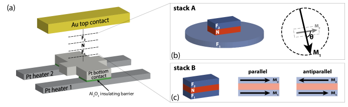
In this paper two types of FNF stacks are used. One for the angle dependent measurements (section IV) and an other for the TSTT measurements (section V), for convenience they are named stack type A (Fig. 1(b)) and B (Fig. 1(c)) respectively. For both stack types the full device consists of a bottom platinum (Pt) contact of 60 nm thick and a 130 nm thick gold (Au) top contact with the FNF stack sandwiched in between (see figure 1(a)). On both sides of the Pt bottom contact Pt Joule heaters of 40 nm thick are placed to produce a thermal gradient across the FNF stack. An 8 nm thick aluminium oxide (Al2O3) layer seperates these Pt heaters from side extensions of the Pt bottom contact, ensuring strong thermal contact between the two but excluding any direct electrical pick up. Around the stack a 150 nm thick layer of polymethyl methacrylate (PMMA) e-beam resist is crosslinked, electrically isolating the top from the bottom contact.
The stack of type A, see figure 1(b), is fabricated in two steps. First a circular F1 layer of 15 nm thick Permalloy (Py)(Ni80Fe20) is deposited, with a diameter of 300 nm. After cleaning the interface by Ar ion milling, to create a good Ohmic contact, the remainder of the stack is deposited consisting of a 10 nm thick copper layer (Cu) followed by a 10 nm thick Py layer with lateral dimensions of nm2. Because F1 is circular there is no preferential in-plane direction for the magnetization. The magnetization of F1 (M1) will therefore easily follow a relatively small rotating applied magnetic field. However, the rectangular shape of F2 ensures an easy axis for M2, parallel to its longest side, due to shape anisotropy. Therefore the rotation of M2 is negligible when the applied field is much lower than the field needed to rotate M2 or to overcome its hard axis direction. Such magnetic behavior is ideal for magnetization angle dependent measurements, further discussed in section IV.
Stacks of type B, see figure 1(c), are rectangular in shape ( nm2) and consists of 15 nm (F1) and 5 nm (F2) thick Py layers separated by a 15 nm thick Cu spacer. The full stack is deposited without breaking vacuum. Both magnetic layers have the same easy axis direction giving two distinct stable states, namely parallel or anti parallel alignment of the two magnetizations. These stacks are used in section V to investigate changes in switching field due to TSTT.
The electrical measurements presented in this paper are all performed using standard lock-in detection techniques, providing a way to distinguish first harmonic response signals () from second harmonic response signals (). To ensure a thermal steady-state condition a low excitation frequency of 17 Hz was used. All measurements are performed at room temperature except for the temperature dependent measurement in section V, where a Peltier heating element together with a thermometer is used to bring and keep the sample at a preset elevated temperature.
IV Angle dependent experiments
To investigate the aMR and aSDSE an FNF stack of type A is used (see Section III). For characterization purposes we first measure the MR and SDSE.
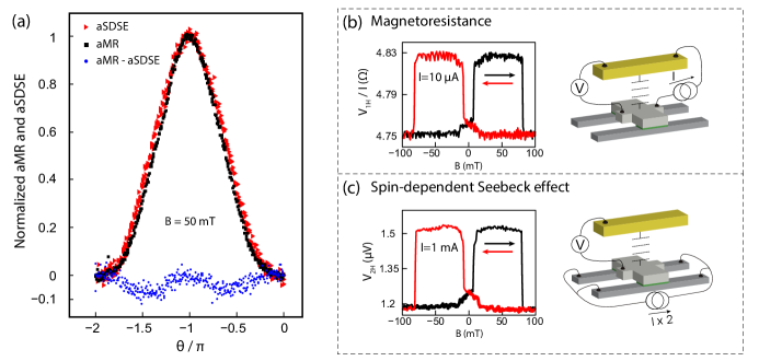
Fig. 2(b) gives the MR measurement where the resistance across the stack is measured as a function of the applied magnetic field (B), parallel to the easy axis of F2. Just after B passes through zero the magnetization in the F1 layer switches as it has no easy axis direction. The field necessary to switch the magnetization of F2 is significantly larger, around 80 mT, as it has to overcome the planar shape anisotropy. Nevertheless the field to switch F2 is larger than expected for a single layer of its size and shape. This is caused by the dipole magnetic field created by the F1 layer coupling to the magnetization of F2. For the angle dependent measurements we have to make sure that this coupling is canceled out such that it will not influence M2 when rotating M1. From separate measurements we conclude that the coupling corresponds to a 50 mT field, see appendix B. A constant B of 50 mT in the angle dependent experiments is therefore sufficient to cancel out the dipole coupling field. Note that because we compare aMR and aSDSE measurements directly, measured on the same sample and using the same technique, any small differences between the angle set by the rotation of B and the actual angle, between M1 and M1, has no effect on the ability to compare both curves.
The MR measurement corresponds well with the results found from a Comsol Multiphysics three-dimensional finite element model (3D-FEM) with and . See Refs. Dejene, 2013; Slachter, 2011 for a full discussion of the model. The difference in Pσ for the two F layers is because of the ion mill cleaning of the F1 layer,Slachter (2010); Dejene (2012) which leads to a stronger spin scattering and can thus be taken as an effective lower Pσ.
The SDSE measurement in Fig. 2(c) gives the Seebeck voltage measured across the stack while sweeping B. The temperature gradient over the stack is produced by sending a 1 mA root mean square current through each Pt Joule heater. A clear difference in the Seebeck voltage for the parallel and antiparallel case is observed. The SDSE signal and the background voltage correspond well with previously reported results Slachter (2010); Dejene (2012) and with the modeled values, with and .
For the angle dependent measurements the sample holder is mounted on a rotatable stage with a rotation precision of at least radian by the automated control of a stepper motor. The sample holder is rotated from to radian with a constant B of 50 mT while recording the voltage across the stack. M1 will follow B therefore creating an angle between M1 and M2, see figure 1(b), equal to the rotation of the sample holder.
In Fig. 2(a) the aMR and aSDSE measurements are plotted together and are normalized by the spin signal from the MR and SDSE measurements, respectively. In this way the angle dependence of both effects can directly be compared. A small but distinct difference between the two curves is visible, as the aSDSE is wider than the aMR, indicating that starts playing a role. From this we can conclude that a SHA builds up in our stacks, verifying previous results of direct SHA measurements.Dejene (2013) The TSTT, as described in Eq. 6, will be affected as well but from the relatively small difference between the aMR and aSDSE curves, of maximum 10% of the total spin signal (see Fig. 2(a)), we can assume that this change will be small and in first order can be neglected.
V Investigation of thermal spin-transfer torque
The existence of an SDSE suggests that the spin current generated by a thermal gradient across an FNF stack would produce a TSTT. The experiments discussed in this section are aimed at finding evidence for such a TSTT. For this purpose we use devices with FNF stack of type B (see Fig. 1(c)) to investigate the changes in minor loop switching fields.
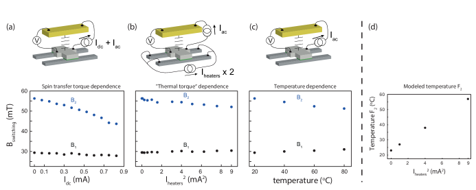
The magnetic minor loop measurement is presented in Fig. 3(a), where the first harmonic response is plotted as a function of B. Here we only look at the switching of the 5 nm thick F2 layer. First M1 and M2 are saturated parallel by applying a high positive magnetic field. Now B is sweeped towards zero until M1 switches, bringing the stack into the anti parallel resistance state. By reversing the B field sweep direction, before M2 switches, a minor loop is obtained when M1 switches back to its original parallel resistance state. The minor loop should normally be centered around B=0 but is shifted to around B=45 mT in our devices, because of the dipole field coupling between the two F layers.
In Fig. 3(b) the STT switching experiment is given for characterization purposes. On top of the small alternating current (I) of 10 A, which gives the resistance of the stack via a lock-in detection technique, a direct current (I) is sent through the stack responsible for inducing the STT. Sweeping I from -1.5 to +1.5 mA a STT switching from the parallel to anti parallel state is observed, for a positive I of 0.8 mA, and a reverse switch, for a negative I of -1.2 mA. A constant B of 40 mT is applied to make sure that we are within the minor loop (Fig. 3(a)), where both the parallel and anti parallel magnetization alignment constitute a stable state.
The experiments discussed above show that the switching fields B1 and B2 in the minor loop are changed by STT, or in other words the barrier going from the P to AP state and vice versa is changed. Measuring these two switching fields as a function of I, through the FNF stack, therefore quantifies the response of the sample to STT, at currents below the STT switching current. Fig. 4(a) gives this evolution of B1 and B2, where every measurement point is an average switching field from 5 consecutively obtained minor loops. B2 clearly shifts to lower values for higher I values, almost reaching 40 mT at an I of 0.8 mA, corresponding well to the STT switching current observed in Fig. 3(b). B1 on the other hand only shows a very small decrease consistent with magnetic phase diagrams found for similar stacks.Krivorotov (2004)
For TSTT a similar change in B1 and B2 should be observed when increasing the temperature gradient across the stack. In the measurement presented in Fig. 4(b) this is investigated by determining these switching fields as a function of I, sent through the Pt Joule heaters. The results are plotted versus I because the Joule heating scales quadratically with I. Indeed a clear quadratic decrease of B2 is observed as one would expect for TSTT. However B1 now seems to slightly increase, instead of showing a small decrease as seen for the STT measurement. This could indicate that the changes in B1 and B2 are not purely due to TSTT, but overall heating of F2 plays an important role as well. Namely, overall heating will lower the coercive field of the F2 layer. To further investigate this we measured the evolution of the switching fields as a function of the overall temperature of the device, without any STT or temperature gradient applied. A heating element together with a thermometer, positioned underneath and in good thermal contact with the sample, was used to controllably set the overall temperature of our device. Fig. 4(c) gives the results up to a temperature of 80C, showing a very similar behavior as the “thermal” STT dependent measurement in Fig. 4(b).
To determine if the results in Fig. 4(b) are dominated by overall heating the temperature of the F2 layer as function of I needs to be known. Experimentally this is difficult to determine and therefore we use our 3D finite element model, successfully used in section IV as well as numerous previously reported measurements.Slachter (2010); Dejene (2012, 2013) The modeled temperature of F2 versus I is given in Fig. 4(d). At an I of 3 mA (I=9 mA2) F2 reaches a temperature of 57 C. The same I gives a B of 52 mT, according to the measurement in Fig. 4(b), which is also found for an overall heating of 60 C in Fig. 4(c). In other words the change in B observed in Fig. 4(b) seems to be dominated by the overall heating of the F2 layer.

VI Discussion and conclusion
The aSDSE measurement presented in section IV shows that the spin heat accumulation in our devices will influence the TSTT, however this changed is assumed to be small and can effectively be neglected. Applying a temperature gradient across an FNF stack, presented in section V, shows no evidence of TSTT. This we attribute to the dominance of overall heating of the magnetic layer, masking the response due to TSTT. If we indeed neglect the relatively small efficiency difference in TSTT and current driven STT, then Eq. 5 and 6 describe the torques, respectively. The needed to produce the same amount of STT, for a certain through the stack, is then found by setting and gives
| (7) |
where R is the resistance of the spin active part of the stack active_part and is the current through the stack as plotted on the x-axis in Fig. 4(a). Using R=1.3 (from the 3D-FEM), S=-18 V/K and for P and P’ the values found in section IV we get; . In order to switch the F2 layer using current driven STT an of 0.8 mA is required (see Fig. 3 (b)), which then corresponds to a of 230 K, across the spin active part active_part of the F1 layer, for pure TSTT driven switching. It can safely be said that such a large steady state cannot be applied across such a short length and will lead to a significant increase in the background temperature. This becomes evident when determining the TSTT versus overall heating contribution in the “thermal torque” dependence measurement (see Fig. 4(b)). For the largest Joule heating current () in Fig. 4(b) B is 52 mT, which corresponds to an I of 0.375 mA for the STT dependent measurement in Fig. 4(a). The change in B observed in Fig. 4(b) would therefore need a of K, across the spin active part of the stack active_part , if caused purely by TSTT. The model gives a K for the largest Joule heating current, which would mean TSTT is only responsible for a maximum of 10% of the observed B change.
In conclusion we can say that although the angle dependent measurements show that a thermal gradient will induce a TSTT, it is small and difficult to distinguish from overall heating effects. Overall heating leads to a lowering of the energy switching barrier for both the P and AP state, such that B1 and B2 move towards each other and gives a narrower minor loop. In the case of STT, either induced by a thermal or voltage gradient, the two switching fields should move in the same direction providing a way to distinguishing it from overall heating. Our results show that, in steady state experiments, it is difficult to avoid overall heating from being the dominant effect, unless the magnetic layer under investigation is connected directly to an almost perfect heat sink. An alternative approach would be to use use short heat pulses and look at time dependent signals as discussed in Ref. Hatami, 2007; Jia, 2011; Leutenantsmeyer, 2013 for tunnel magnetoresistance (TMR) structures.
A combined effect of the lowering of the switching barrier by overall heating together with TSTT could of course be beneficial as the torque needed to switch will be smaller. This route is currently being investigated in the form of heat assisted switching devices.Beech (2000); Wang (2004); Xi (2010) However it requires an in depth investigation and precise calibration of the timing of the two effects.
Acknowledgements.
We would like to acknowledge B. Wolfs, M. de Roosz and J. G. Holstein for technical assistance. This work is part of the research program of the Foundation for Fundamental Research on Matter (FOM) and supported by NanoLab NL and the Zernike Institute for Advanced Materials.Appendix A aMR and aSDSE formula’s
Appendix B Dipole magnetic field coupling
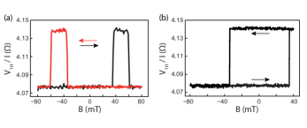
To determine the dipole field coupling between the F1 and F2 layer for stack type A similar devices were fabricated, with a 1.5 m by 100 nm rectangular F1 layer. As the F1 layer is now much longer than the F2 layer the dipole coupling field will become negligibly small. As the rest of the device and especially the N and F2 layer are kept the same we are able to determine the switching field of F2 without any coupling present. In Fig. 5 the spin valve and minor loop measurements are given. The minor loop is perfectly centered around B=0 confirming that the dipole field coupling is negligibly small. Furthermore we observe a switching field of 35 mT, which can be seen as the uncoupled switching field. Comparing this to the switching field of 85 mT for the coupled stacks used in the angle dependent measurements, see Fig. 2, we estimate a dipole coupling field of 50 mT.
References
- Slonczewski (1996) J. C. Slonczewski, Journ. of Magn. and Magn. Mater. 159, L1-L7 (1996).
- Berger (1996) L. Berger, Phys. Rev. B 54, 9353 (1996).
- Åkerman (2005) J. Åkerman, Science 308, 508-510 (2005).
- Valet (1993) T. Valet, A. Fert, Phys. Rev. B 48, 7099 (1993).
- Brataas et al. (2000) A. Brataas, Yu. V Nazarov, G. E. W. Bauer, Phys. Rev. Lett. 84, 2481 (2000).
- Brataas et al. (2006) A. Brataas, G. E. W. Bauer, P. J. Kelly, Phys. Rep. 427, 157 (2006).
- Kovalev (2002) A. A. Kovalev, A. Brataas, G. E. W. Bauer, Phys. Rev. B 66, 224424 (2002).
- Urazhdin (2005) S. Urazhdin, R. Loloee, W. P. Pratt, Jr., Phys. Rev. B 71, 100401(R) (2005).
- Bauer (2012) G. E. W. Bauer, E. Saitoh, B. J. van Wees, Nature Materials 11, 391 (2012).
- Slachter (2010) A. Slachter, F. L. Bakker, J-P. Adam, B. J. van Wees, Nature Physics 6, 879 (2010).
- Dejene (2012) F. K. Dejene, J. Flipse, B. J. van Wees, Phys. Rev. B 86, 024436 (2012).
- Yu (2010) H. Yu, S. Granville, D. P. Yu, J.-Ph. Ansermet, Phys. Rev. Lett. 104, 146601 (2010).
- Kovalev (2006) A. A. Kovalev, G. E. W. Bauer, A. Brataas, Phys. Rev. B 73, 054407 (2006).
- Hatami (2007) M. Hatami, G. E. W. Bauer, Q. Zhang, P. J. Kelly, Phys. Rev. Lett. 99, 066603 (2007).
- (15) The spin active part consists of the F layers for a thickness equal to the spin relaxation length () .
- Heikkila (2010) T. T. Heikkilä, M. Hatami, G. E. W. Bauer, Phys. Rev. B 81, 100408(R) (2010).
- Dejene (2013) F. K. Dejene, J. Flipse, G. E. W. Bauer, B. J. van Wees, Nature Physics 9, 636-639 (2013).
- (18) L. Giacomoni, B. Dieny, W. P. Pratt, Jr., R. Loloee, M. Tsoi, (unpublished) .
- Slachter (2011) A. Slachter, F. L. Bakker, B. J. van Wees, Phys. Rev. B 84, 174408 (2011).
- Krivorotov (2004) I. N. Krivorotov, N. C. Emley, A. G. F. Garcia, J. C. Sankey, S. I. Kiselev, D. C. Ralph, R. A. Buhrman, Phys. Rev. Lett. 93, 166603 (2004).
- Jia (2011) X. Jia, K. Xia, G. E. W. Bauer, Phys. Rev. Lett. 107, 176603 (2011).
- Leutenantsmeyer (2013) J. C. Leutenantsmeyer, M. Walter, V. Zbarsky, M. Münzenberg, R. Gareev, K. Rott, A. Thomas, G. Reiss, P. Peretzki, H. Schuhmann, M. Seibt, M. Czerner, C. Heiliger, SPIN 03, 1350002 (2013).
- Beech (2000) R. S. Beech, J. A. Anderson, A. V. Pohm, J. M. Daughton, J. Appl. Phys. 87, 6403 (2000).
- Wang (2004) J. Wang, P. P. Freitas, Appl. Phys. Lett. 84, 945 (2004).
- Xi (2010) H. Xi, J. Stricklin, H. Li, Y. Chen, X. Wang, Y. Zheng, Z. Ghao, M. X. Tang, IEEE Trans. Magn. 46, 860 (2010).