Large-scale BN tunnel barriers for graphene spintronics
Abstract
We have fabricated graphene spin-valve devices utilizing scalable materials made from chemical vapor deposition (CVD). Both the spin-transporting graphene and the tunnel barrier material are CVD-grown. The tunnel barrier is realized by h-BN, used either as a monolayer or bilayer and placed over the graphene. Spin transport experiments were performed using ferromagnetic contacts deposited onto the barrier. We find that spin injection is still greatly suppressed in devices with a monolayer tunneling barrier due to resistance mismatch. This is, however, not the case for devices with bilayer barriers. For those devices, a spin relaxation time of 260 ps intrinsic to the CVD graphene material is deduced. This time scale is comparable to those reported for exfoliated graphene, suggesting that this CVD approach is promising for spintronic applications which require scalable materials.
Introduction
Owing to its small spin-orbit coupling, negligible hyperfine interaction, and unparalleled high carrier mobility at room temperature, Novoselov04 ; Wang13 ; Seneor2012 ; Dlubak2012 graphene is predicted to be the ideal material for spintronic applications. Research conducted on graphene spintronics so far has focused mostly on epitaxial or exfoliated high-mobility graphene with various oxide-based tunnel barriers. Dankert2014 ; Birkner2013 ; Volk2013 ; Idzuchi2014 ; Tombros2007 ; Popinciuc2009 ; Han2011 ; Yang2011 ; Droegeler2014 ; Zomer2012 ; Dlubak2012b ; Guimaraes2012 Spin relaxation times up to ns Yang2011 ; Droegeler2014 and spin transport in graphene over record distances of 20 m Zomer2012 have been demonstrated in four-terminal non-local measurement geometries at room temperature. Very recently, spin relaxation lengths up to hundreds of m have also been reported in two-terminal devices (local measurement geometry). Dlubak2012 ; Seneor2012 However, in order to achieve scalable devices, large-area graphene, as for example provided by chemical vapor deposition (CVD) is required. Li2009 CVD graphene devices with Al2O3 tunnel barriers have been fabricated which exhibited spin relaxation lengths comparable to those reported for exfoliated graphene, Avsar2011 showing their potential for future applications.
Although these achievements are already quite remarkable, they are still far from theoretical expectations based on the low spin-orbit interaction and hyperfine coupling of graphene. Guimaraes2012 Several recent studies suggest that the performance of lateral graphene spin valves is still limited by the quality of the tunnel barriers in many devices. Dlubak2012 ; Seneor2012 ; Idzuchi2014 ; Droegeler2014 ; Sosenko2014 It is known that pin-holes can be formed in oxide barriers due to inhomogeneous wetting of the oxide layer on the hydrophobic graphene surface. Dlubak2012b This can diminish the spin injection due to resistance mismatch. To achieve a more homogeneous coverage, several groups have tried to functionalize graphene before growing the oxide. Dlubak2012b ; Wang2008 ; Robinson2010 However, this merely reduces the chances of pin-hole formation but cannot rule them out. Pin-holes can still appear. One of the solutions to this problem is to use a two-dimensional (2D), atomically thin insulator with perfect crystalline structure that can be placed onto graphene. Novoselov2005 Hexagonal boron nitride (h-BN), which possesses a large band gap (5.97 eV) and has a small lattice mismatch to graphene, Wang13 ; Britnell2012 ; Meric2013 is a promising candidate. Very recently, Yamaguchi et al. have demonstrated exfoliated h-BN as tunnel barrier for spin injection and detection in exfoliated lateral graphene spin valve devices. Yamaguchi2013
In the present work, we combine layered tunnel barriers with scalable fabrication by using large-area CVD h-BN as tunnel barriers for CVD graphene-based lateral spin valves. We have performed both local and non-local spin-valve measurements on the same devices, and obtained spin relaxation times and tunnel barrier resistances similar to those reported previously for exfoliated graphene samples with exfoliated h-BN tunnel barriers, suggesting that CVD graphene with CVD h-BN tunnel barrier is a promising system for large-scale spintronic applications.
Experimental methods
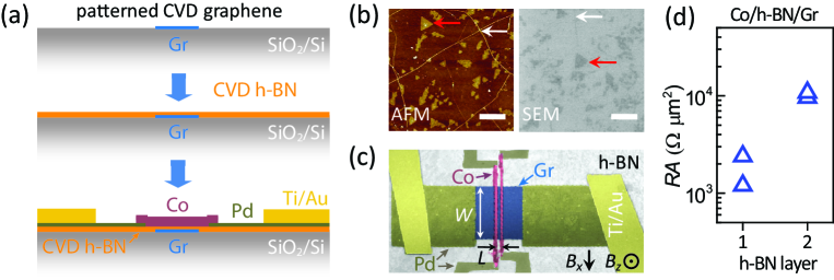
To obtain graphene/h-BN heterostructures, we have performed a sequential transfer of CVD graphene and CVD h-BN, followed by electrode fabrication. We start with large-area CVD graphene, which we have grown on Cu. Fu2011 As shown in Fig. 1a, the graphene layer was first transferred onto a Si substrate with a SiO2 top layer 285 nm in thickness and then patterned into micron-wide ribbons using standard electron beam lithography (EBL) and oxygen plasma etching. Then, a uniform monolayer (ML) of CVD h-BN GrapheneSupermarket is transferred onto graphene using the same transfer technique as for CVD graphene. Li2009 Both atomic force microscopy (AFM) and scanning electron microscopy (SEM) images suggest the presence of a uniform ML h-BN with a multilayer coverage of less than 20 . This is shown in Fig 1b, where the red arrows indicate multilayer regions with triangular shape, whereas the white ones show grain boundaries. A bilayer (BL) h-BN tunnel barrier can be obtained by repeating the transfer process a second time.
In order to minimize the oxidation of the ferromagnetic electrodes, the Co strips (50 nm in thickness and 150 or 300 nm in width) are placed in the final fabrication step. These strips are connected to normal metal contacts made from Ti/Au (5 nm/45 nm) by an intermediate thin Pd strip (10 nm). The non-magnetic contacts to graphene are also made from similar thin Pd strips connected to thicker Ti/Au leads. Fig. 1c shows a false-color SEM image of a CVD graphene-based lateral spin valve device with a CVD h-BN tunnel barrier. Four samples will be addressed in this study: a device with an ML h-BN tunnel barrier and a graphene channel of length m denoted as ML1, and three BL h-BN devices with different channel lengths of 1, 2, and 3 m, denoted as BL1, BL2, and BL3. The three BL h-BN samples were fabricated together in the same batch.
Results and discussion
We characterize the Co/h-BN/graphene junction resistances using three-terminal measurements. Fig. 1d shows the obtained resistance-area product of 1-3 k m2 for sample ML1 (1 k for contact areas of 2.4 m2 and 1.2 k for contact areas of 1.2 m2) and 10 k m2 for sample BL1 (4 k for 2.4 m2 and 9 k for 1.2 m2), measured within a 1-10 mV bias voltage range. These values are comparable to previously reported products of exfoliated h-BN tunnel barriers, Yamaguchi2013 suggesting that we have successfully fabricated tunnel barriers from CVD-grown h-BN between the ferromagnetic layer and graphene.
At 4.2 K, all three BL h-BN samples show similar dependencies of the resistivity of graphene on the back-gate voltage obtained by local four-terminal measurements. Fig. 2b depicts the curve, as well as the corresponding conductivity (solid grey line), deduced from local four-terminal measurement of the BL3 sample. At a back-gate voltage =0 V, we find =3.6 k. To estimate the carrier mobility we use the basic transport equation , where is the electron charge and the carrier density. The charge density is proportional to the gate voltage measured from the charge-neutrality point (CNP), =14 V, with a proportionality constant given by the gate capacitance . Explicitly, we obtain through the relation , where is the slope of the curve taken at negative gate voltages far away from the CNP (see Fig. 2b solid red line). We obtain 850 cm2V-1s-1.
Fig. 2a shows the schematic circuit for the non-local magneto-resistance (MR) measurements. Johnson1985 A current is injected from Co2 to Pd2 and a non-local voltage is measured between Co1 and Pd1. The non-local resistance is defined as the ratio of non-local voltage and the local current , i.e. . In this setup, the charge current is separated from the voltage measurement circuit, and only the spin current, which is injected at Co2 and diffusing outside of the current path, is detected by Co1 at a distance of .
The in-plane magnetic field () dependence of the measured non-local resistance for sample ML1 and BL1 at a gate voltage of =0 V is shown in Fig. 2c. Due to different widths of the two ferromagnetic contacts (150 nm and 300 nm), the ferromagnets switch at different fields, yielding a magnetic field range in which the magnetic moments of the two contacts have an antiparallel alignment. The difference in observed for parallel and antiparallel alignment defines the MR value. The solid arrows indicate the polarization direction of Co1 and Co2, and the horizontal arrows show the sweeping direction of the magnetic field. Positive (negative) non-local voltage is observed when the polarizations of the two ferromagnetic strips are parallel (antiparallel). vanSon1987 The measurements are performed using the standard a.c. lock-in technique with a relatively large supplied current 10 A to obtain a good signal-to-noise ratio. On sample ML1, we also performed non-local MR measurements at 300 K. Clear non-local MR signals are observed at both 4.2 K and 300 K (Fig. 2c), indicating electrical spin injection from the ferromagnet to CVD graphene through the CVD h-BN tunnel barriers over a wide temperature range. At 4.2 K, device ML1 with low contact resistances (1 k) exhibits a relatively small non-local MR signal of only 40 m. With higher h-BN thickness and otherwise identical parameters, device BL1 exhibits much higher contact resistances (9 k) and shows an in-plane non-local MR signal of 1.6 (Fig. 2b). This suggests that the observed, relatively small non-local MR signal in case of an ML CVD h-BN tunnel barrier is most likely limited by resistance mismatch at the ferromagnetic contacts.
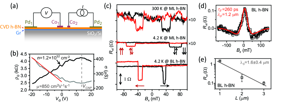
A reliable determination of the spin relaxation time can be accomplished by measuring the Hanle effect, the precession and dephasing of spins in an out-of-plane magnetic field . Johnson1985 We first polarized the ferromagnetic electrodes in either parallel or antiparallel alignment by choosing a suitable in-plane magnetic field . Then, the non-local resistances were recorded as a function of for both conditions. To eliminate any spurious contributions due to Hall effect or other MR effects, we determined the Hanle curve by subtracting the parallel from antiparallel measurement curves. Fig. 2d depicts such a difference Hanle curve (at 4.2 K) for sample BL3 measured at 0 V. This curve can be fitted by using the solution of the diffusion equation: Jedema2002
where is the spin diffusion constant, the electron g-factor set to 2 in the fit, the electron Bohr magneton, the reduced Planck constant, and the diffusion time. For this fit, in addition to the g-factor, we fix by an estimate obtained from the conductivity using the Einstein relation , where is the graphene density of states at the Fermi energy . This later quantity can be expressed by using the energy-momentum dispersion relation of idealized graphene with a Fermi velocity of m/s. We obtain 55 cm2s-1 at 0 V where the carrier density is cm-2. The Hanle fit (solid red curve in Fig. 2d) results in a spin relaxation time of 260 ps, corresponding to a spin relaxation length of 1.2 m. This is comparable to previous results obtained on CVD graphene as well as exfoliated graphene samples on SiO2/Si substrate. Popinciuc2009 ; Avsar2011
One can also obtain an estimate for by looking at the absolute value of for samples BL1-BL3 that were fabricated together in one batch, but have different channel lengths . For these samples with bilayer h-BN tunneling barriers, the contact resistances k are larger than the graphene channel resistance determined over a spin-relaxation length. This so called spin-relaxation resistance is given by , yielding k with the width of the graphene flake m. In this regime, where resistance mismatch is not an issue, should follow the relation: Jedema2002
where is the spin polarization of the injector contact. The measured three values for are plotted in Fig. 2e on a logarithmic scale as a function of . From the decaying slope we deduce 1.60.4 m at 4.2 K. This is in good agreement with the relaxation length obtained from the non-local Hanle measurement discussed before.
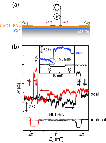
After evaluating the non-local MR characteristics of the CVD graphene-based lateral spin valve devices with CVD h-BN tunnel barriers, we were also able to perform two terminal local MR measurements on the same samples, see Fig. 3a. Recently, Dlubak et al. Dlubak2012 deduced exceptionally long spin relaxation lengths exceeding hundreds of m based on local MR measurements on two terminal graphene spin valve devices with graphene channels of only a few m in length. However, they have not performed non-local or Hanle measurements. It is therefore instructive to compare non-local with local MR measurements. Fig. 3b shows such a comparison on samples BL1 and ML1 (inset). The jumps in the local resistances occurred at very similar switching fields to those of the non-local resistance, but with opposite sign and different magnitude. The difference in sign is what one expects in a simplified model. For the local MR, an antiparallel alignment of the magnetizations of the two Co strips will lead to a resistance increase which is explained by the two channel current model, similar to the tunneling MR (TMR) effect. vanSon1987 In the non-local measurement, a positive non-local voltage is expected if both the injector and detector contact are aligned in parallel, and a negative one in the opposite case. The local measurement also exhibits a larger noise floor. While the spin and the charge current paths are spatially separated in the non-local measurement, the spin accumulation in the local geometry is detected in the presence of the charge current background. This gives rise to the observed noise floor as well as to an additional feature (grey circle in the inset of Fig. 3b), which is possibly caused by the anisotropic MR (AMR) contribution of the magnetic contacts. Aurich2010
For the interpretation of these measurements, we use the spin relaxation length 1.2 m deduced before, obtaining 0.54 k9 k in the BL h-BN devices, which suggests that spin relaxation inside the graphene channel dominates. From the local MR measurements on sample BL1 we found 6.6 at =0 V. This value is about 4 times as large as the non-local MR spin signal of 1.6 at the same gate voltage. This is interesting as the simple theory would predict only a factor of 2 difference. Seneor2012 The measurements on sample ML1 shown in the inset of Fig. 3b yield a similar result: 0.4 and 0.1 , which also amounts to a factor of 4. The explanation of this result requires further studies.
Conclusions
In conclusion, we have assembled scalable spin valve devices using large-scale CVD graphene as transport material and large-scale CVD h-BN as tunnel barrier. During our studies of spin-transport properties, we have found spin relaxation times comparable to those reported for exfoliated graphene samples fabricated on SiO2/Si substrates. Moreover, we have shown that both local and non-local measurements can be performed on the same device. Further investigations in this direction can shed light on the spin relaxation mechanism which is still not completely understood in graphene. We believe that this work paves the way for further research on graphene spintronic devices based on large-scale 2D heterostructures. After finishing the manuscript we became aware of a similar work on exfoliated graphene with CVD h-BN tunnel barriers. VenkataKamalakar2014
Acknowledgements.
The authors acknowledge funding from the Swiss National Science Foundation (SNF), ESF Eurographene, NCCR-QSIT, the FP7 project SE2ND, ERC QUEST, the Swiss Nanoscience Institute (SNI) and Graphene Flagship. The authors also wish to thank Bernd Beschoten, Takis Kontos, Andreas Baumgartner, Jörg Gramich, Julia Samm, and Simon Zihlmann for helpful discussions. Wangyang Fu and Péter Makk contributed equally to this work.References
- (1) K. S. Novoselov, A. K. Geim, S. V. Morozov, D. Jiang, Y. Zhang, S. V. Dubonos, I. V. Grigorieva, and A. A. Girsov, Electric field effect in atomically thin carbon films. Science 2004, 306, 666.
- (2) L. Wang, I. Meric, P. Y. Huang, Q. Gao, Y. Gao, H. Tran, T. Taniguchi, K. Watanabe, L. M. Campos, D. A. Muller, J. Guo, P. Kim, J. Hone, K. L. Shepard, and C. R. Dean, One-dimensional electrical contact to a two-dimensional material. Science 2013, 342, 614.
- (3) P. Seneor, B. Dlubak, M.-B. Martin, A. Anane, H. Jaffres, and A. Fert, Spintronics with graphene. MRS Bulletin 2012, 37, 1245.
- (4) B. Dlubak, M.-B. Martin, C. Deranlot, B. Servet, S. Xavier, R. Mattana, M. Sprinkle, C. Berger, W. A. De Heer, F. Petroff, A. Anane, P. Seneor, and A. Fert, Highly efficient spin transport in epitaxial graphene on SiC. Nat. Phys. 2012, 8, 557.
- (5) A. Dankert, M. V. Kamalakar, J. Bergsten, and S. P. Dash, Spin transport and precession in graphene measured by nonlocal and three-terminal methods. Appl. Phys. Lett. 2014, 104, 192403.
- (6) B. Birkner, D. Pachniowski, A. Sandner, M. Ostler, T. Seyller, J. Fabian, M. Ciorga, D. Weiss, and J. Eroms, Annealing-induced magnetic moments detected by spin precession measurements in epitaxial graphene on SiC. Phys. Rev. B 2013, 87, 081405(R).
- (7) C. Volk, C. Neumann, S. Kazarski, S. Fringes, S. Engels, F. Haupt, A. Müller, and C. Stampfer, Probing relaxation times in graphene quantum dots. Nat. Commu. 2013, 4, 1753.
- (8) H. Idzuchi, Y. Fukuma, S. Takahashi, S. Maekawa, and Y. Otani, Effect of anisotropic spin absorption on the Hanle effect in lateral spin valves. Phys. Rev. B 2014, 89, 081308(R).
- (9) N. Tombros, C. Jozsa, M. Popinciuc, H. T. Jonkman, and B. J. van Wees, Electronic spin transport and spin precession in single graphene layers at room temperature. Nature 2007, 448, 571.
- (10) M. Popinciuc, C. Józsa, P. J. Zomer, N. Tombros, A. Veligura, H. T. Jonkman, and B. J. van Wees, Electronic spin transport in graphene field-effect transistors. Phys. Rev. B 2009, 80, 214427.
- (11) W. Han and R. K. Kawakami, Spin relaxation in single-layer and bilayer graphene. Phys. Rev. Lett. 2011, 107, 047207.
- (12) T.-Y. Yang, J. Balakrishnan, F. Volmer, A. Avsar, M. Jaiswal, J. Samm, S. R. Ali, A. Pachoud, M. Zeng, M. Popinciuc, G. Güntherodt, B. Beschoten, and B. Özyilmaz, Observation of long spin-relaxation times in bilayer graphene at room temperature. Phys. Rev. Lett. 2011, 107, 047206.
- (13) M. Drögeler, F. Volmer, M. Wolter, B. Terrés, K. Watanabe, T. Taniguchi, G. Gütherodt, C. Stampfer, and B. Beschoten, Nanosecond spin lifetimes in single- and few-layer graphene-hBN heterostructures at room temperature. arXiv:1406.2439 2014.
- (14) P. J. Zomer, M. H. D. Guimares, N. Tombros, and B. J. van Wees, Long-distance spin transport in high-mobility graphene on hexagonal boron nitride. Phys. Rev. B 2012, 86, 161416(R).
- (15) B. Dlubak, P. R. Kidambi, R. S. Weatherup, S. Hofmann, and J. Robertson, Substrate-assisted nucleation of ultra-thin dielectric layers on graphene by atomic layer deposition. Appl. Phys. Lett. 2012, 100, 173113.
- (16) M. H. D. Guimares, A. Veligura, P. J. Zomer, T. Maassen, I. J. Vera-Marun, N. Tombros, and B. J. van Wees, Spin transport in high-quality suspended graphene devices. Nano Lett. 2012, 12, 3512.
- (17) X. S. Li, W. W. Cai, J. An, S. Kim, J. Nah, D. X. Yang, R. Piner, A. Velamakanni, I. Jung, E. Tutuc, S. K. Banerjee, L. Colombo, and R. S. Ruoff, Large-area synthesis of high-quality and uniform graphene films on copper foils. Science 2009, 324, 1312.
- (18) A. Avsar, T. Yang, S. Bae, J. Balakrishnan, F. Volmer, M. Jaiswal, Z. Yi, S. R. Ali, G. Guüntherodt, B. H. Hong, B. Beschoten, and B. Özyilmaz, Toward wafer scale fabrication of graphene based spin valve devices. Nano Lett. 2011, 11, 2363.
- (19) E. Sosenko, H. Wei, and V. Aji, Effect of contacts on spin lifetime measurements in graphene. Phys. Rev. B 2014, 89, 245436.
- (20) W. H. Wang, W. Han, K. Pi, K. M. McCreary, F. Miao, W. Bao, C. N. Lau, and R. K. Kawakami, Growth of atomically smooth MgO films on graphene by molecular beam epitaxy. Appl. Phys. Lett. 2008, 93, 183107.
- (21) J. A. Robinson, M. LaBella, K. A. Trumbull, X. Weng, R. Cavelero, T. Daniels, Z. Hughes, M. Hollander, M. Fanton, and D. Snyder, Epitaxial graphene materials integration: effects of dielectric overlayers on structural and electronic properties. ACS Nano 2010, 4, 2667.
- (22) K. S. Novoselov, D. Jiang, F. Schedin, T. J. Booth, V. V. Khotkevich, S. V. Morozov, and A. K. Geim, Two-dimensional atomic crystals. Proc. Natl. Acad. Sci. USA 2005, 102, 10451.
- (23) L. Britnell, R. V. Gorbachev, R. Jalil, B. D. Belle, F. Schedin, M. I. Katsnelson, L. Eaves, S. V. Morozov, A. S. Mayorov, N. M. R. Peres, A. H. Castro Neto, J. Leist, A. K. Geim, L. A. Ponomarenko, and K. S. Novoselov, Electron tunneling through ultrathin boron nitride crystalline barriers. Nano Lett. 2012, 12, 1707.
- (24) I. Meric, C. R. Dean, N. Petrone, L. Wang, J. Hone, P. Kim, and K. L. Shepard, Graphene field-effect transistors based on boron nitride dielectrics. Proc. IEEE 2013, 101, 1609.
- (25) T. Yamaguchi, Y. Inoue, S. Masubuchi, S. Morikawa, M. Onuki, K. Watanabe, T. Taniguchi, R. Moriya, and T. Machida, Electrical spin injection into graphene through monolayer hexagonal boron nitride. Appl. Phys. Exp. 2013, 6, 073001.
- (26) W. Fu, C. Nef, O. Knopfmacher, A. Tarasov, M. Weiss, M. Calame, and C. Schönenberger, Graphene transistors are insensitive to pH changes in solution. Nano Lett. 2011, 11, 3597.
- (27) Single layer h-BN (Boron Nitride) film grown on copper foil. https://graphene-supermarket.com/.
- (28) M. Johnson and R. H. Silsbee, Interfacial charge-spin coupling: Injection and detection of spin magnetization in metals. Phys. Rev. Lett. 1985, 55, 1790.
- (29) P. C. van Son, H. van Kempen, and P. Wyder, Boundary resistance of the ferromagnetic-nonferromagnetic metal interface. Phys. Rev. Lett. 1987, 58, 2271.
- (30) F. J. Jedema, H. B. Heersche, A. T. Filip, J. J. A. Baselmans, and B. J. van Wees, Electrical detection of spin precession in a metallic mesoscopic spin valve. Science 2002, 416, 713.
- (31) H. Aurich, A. Baumgartner, F. Freitag, A. Eichler, J. Trbovic, and C. Schönenberger, Permalloy-based carbon nanotube spin-valve. Appl. Phys. Lett. 2010, 97, 153116.
- (32) M. Venkata Kamalakar, A. Dankert, J. Bergsten, T. Ive, and S. P. Dash, Enhanced tunnel spin injection into graphene using chemical vapor deposited hexagonal boron nitride. arXiv:1406.5827 2014.