Reversible mechanical and electrical properties of ripped graphene
Abstract
We examine the mechanical properties of graphene devices stretched on flexible elastomer substrates. Using atomic force microscopy, transport measurements, and mechanics simulations, we show that micro-rips form in the graphene during the initial application of tensile strain; however subsequent applications of the same tensile strain elastically open and close the existing rips. Correspondingly, while the initial tensile strain degrades the devices’ transport properties, subsequent strain-relaxation cycles affect transport only moderately, and in a largely reversible fashion, yielding robust electrical transport even after partial mechanical failure.

I Introduction
Recent advances in graphene productionKim et al. (2009); Bae et al. (2010); Lee et al. (2010) have enabled the fabrication of a variety of flexible, graphene-based electronic components, including transparent interconnectsKim et al. (2011), high-performance capacitorsEl-Kady et al. (2012), and transistorsLee et al. (2011). The prospect of flexible, graphene-based electronic devices suggested by these results raises an important question: are graphene’s electrical properties and mechanical integrity robust under the strains graphene is likely to experience in such devices? Pristine graphene has an exceptionally high breaking strengthLee et al. (2008), yet it may be susceptible to ripping, particularly if it has defects Kim et al. (2012) and/or strong surface adhesionSen et al. (2010). It is still relatively unknown under what strain conditions substrate-supported graphene rips, and how the electrical properties are then altered.
In this Letter, we combine atomic force microscopy (AFM), coarse-grained mechanical simulations, and electrical transport measurements to study the effects of lateral strain on rips in graphene. We find that graphene adhered to a flexible substrate and then stretched laterally can develop small rips with only 1% applied strain. However, even with ripping, the electrical properties remain relatively robust: introducing small rips slightly increases the resistance, but subsequent strain-relaxation cycles over the same strain range change transport only modestly, and in a largely reversible fashion. Such resilience is atypical for conducting thin films, which typically demonstrate rapid and irreversible device failure after the onset of rip formationCairns et al. (2000); Fortunato et al. (2002).
II Experimental Details
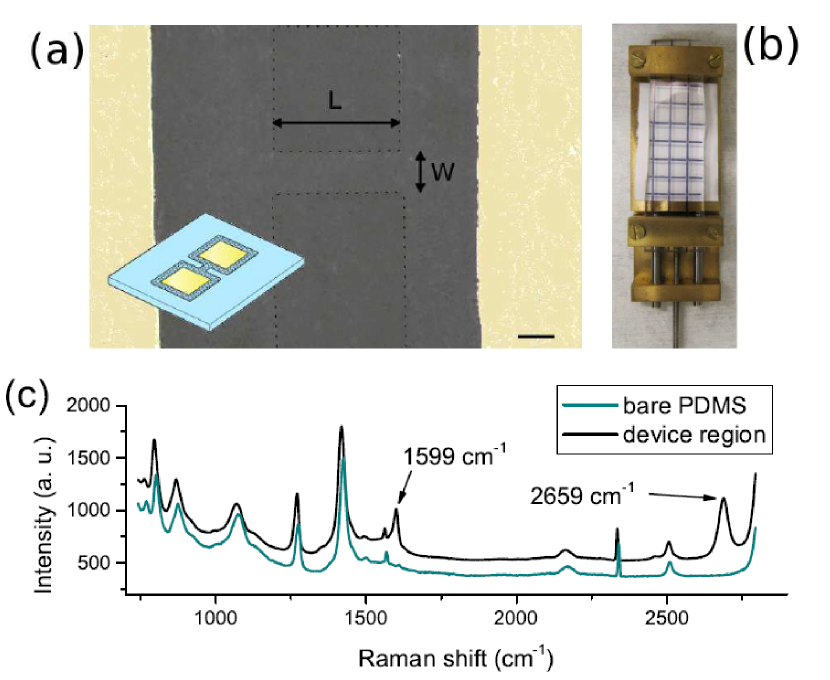
Devices consisted of patterned graphene placed on flexible polydimethylsiloxane (PDMS) substrates. The devices were fabricated using a modified transfer printing process, similar to that described in Ref Kim et al., 2009. Single-layer graphene was grown using established chemical vapor deposition (CVD) techniques Li et al. (2009), and then transferred to a copper-coated silicon wafer where it was patterned using photolithography and reactive ion etching. Next, a piece of PDMS was mechanically pressed onto the silicon wafer, and the copper was then etched to leave patterned graphene on the PDMS substrateLee et al. (2010). Raman spectroscopy was used to confirm the presence of graphene on the PDMS as shown in Figure 1c; the shape of the Raman 2D peakFerrari et al. (2006), as well as subsequent AFM measurements verified the single-layer character of the graphene. Finally, shadow-mask evaporation was used to deposit Ti/Au contact pads. The device geometry is illustrated in Figure 1a: a narrow graphene bridge connects two large graphene pads, each of which is covered with a Ti/Au contact pad. We studied 13 different devices having bridge aspect ratios ranging from 1.5:1 to 12:1 (length:width) and widths of 100, 50, and 25 m. The data in this manuscript focuses on a device with a bridge width of 25 m and an aspect ratio of 2:1. The data for all samples yielded similar qualitative results. Quantitative differences in transport data between different devices were uncorrelated with the bridge dimensions, and instead seemed to be dominated by pre-existing rips in the graphene, which are often introduced during the graphene transfer processKim et al. (2012).
AFM and transport measurements were performed while the PDMS substrate was mounted in a mechanical stretching stage, as shown in Figure 1b. The substrate was clamped at either end, and then strained by turning the threaded rod, which laterally moves the sliding clamp along its guide rails. A mechanical stepper motor was used to control the stretching stage position to ensure reproducibility. Variable device positioning on the substrate as well as slight variations in substrate thickness preclude exact conversion between strain applied to the substrate and to the device, therefore ‘turns of the stretching stage control rod’ were used as the controlled variable. Each turn strains the substrate by approximately one percent, and we estimate that the strain applied to the graphene differs from that applied to the PDMS substrate by no more than ten percent. However, our conclusions are unaffected by this uncertainty, as variations in the magnitude of applied strain between devices only shift the strain axis of the data while preserving the observed trends. Optical observations indicated that the Ti/Au pad adhesion to the substrate was robust and did not slip during measurements. Transport measurements were performed by placing micro-manipulator probes in contact with the gold contact pads at each strain value, and AFM measurements were performed with an Asylum Research MFP-3D.
III Results and Discussion
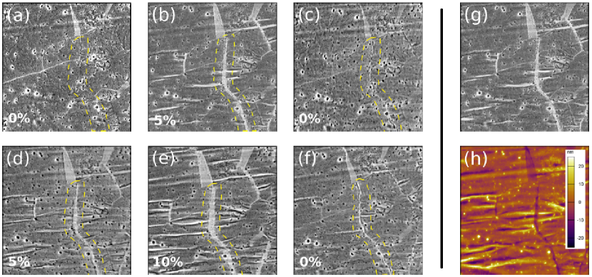
Figures 2a-f show AFM phase images of graphene in the bridge region of a device at 0, 5, 0, 5, 10, and 0 percent strain applied along the horizontal axis of the images. Both rips and delaminations caused by wrinkles appear as a function of strain, and can be distinguished via AFM height data: Figs. 2g and 2h show that wrinkles have corresponding undulations in the height data (peaks and dips) while rips are indicated by a uniform depression (consistent with the substrate exposed between graphene regions). In Fig. 2, the vertical features are rips and the majority of the horizontal features are wrinkles.
The opening and closing of rips is clear in the Figure: the unstrained device (Fig. 2a) exhibits some small rips and defects. When the substrate is mechanically stretched (Fig. 2b) the existing rips widen and new rips form; when the applied strain is relaxed (Fig. 2c), pre-existing defects return to nearly their original condition and newly formed rips close. Subsequent strain-relaxation cycles over the same strain range re-open existing rips (Fig. 2d), but proceeding to a higher strain range forms new rips and widens pre-existing ones (Fig. 2e), which then close less completely when the strain is relaxed (Fig. 2f). The strain values at which we observe micro-rip formation are substantially lower than the reported fracture strength of grapheneLee et al. (2008), however the tensile strength of graphene is strongly susceptible to defects such as holes and tearsLee et al. (2013). Although graphene produced by CVD is known to be polydomain, it has been shown that rips in graphene do not preferentially follow grain boundariesKim et al. (2012). Rather, the fabrication procedures used to generate patterned graphene devices on polymer substrates routinely introduce rips and other defects in the graphene, which accounts for the mechanical failure observed at low strain values.
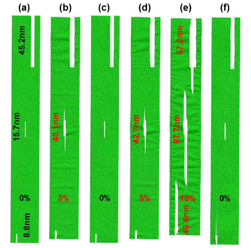
To shed light on the underlying mechanism of the rip formation and evolution, we simulate rip formation and the subsequent elastic opening and closing of rips in graphene, via a coarse-grained (CG) modeling schemeZhu, Huang, and Li (2014). Given the prohibitive simulation expense to model rips of real size in experiments (microns in length), we simulate a scaled-down model of a graphene monolayer with a size of 24 nm by 200 nm (Fig. 3). Three pre-cracks of various sizes are introduced in the model (Fig. 3a) to mimic the pre-existing defects in the as-made sample. Each CG bead in the graphene interacts with a virtual substrate via a Lennard-Jones potentialScharfenberg et al. (2011) , where and , which gives rise to an adhesion energy around 0.044 eV/nm2. In addition, the CG beads on the four outer edges of the simulation model are not allowed to slide relative to the substrate so that the tensile loading of the graphene can be applied by stretching the substrate along the horizontal direction, similar to the experimental setup.
As the applied tensile strain first increases to 5%, the stress concentration near the tips of the short middle crack (15.7 nm in length) becomes sufficiently high to cause the propagation of the short crack in both directions. Due to the nature of displacement loading, the driving force for crack propagation decreases as the crack extends. As a result, the middle crack stops advancing at a length of 40.1 nm (Fig. 3b). Upon unloading of the tensile strain the elongated middle crack closes, nearly fully recovering the original shape of the graphene (Fig. 3c); however, the atomic bond breaking in graphene during crack propagation is not reversible. Consequently, the graphene cannot fully recover its original mechanical integrity.
Further tensile loading up to 5% causes the cracks to reopen but further extension of the cracks is shown to be negligible (Fig. 3d), largely due to a lack of sufficient driving force for crack propagation. The application of a tensile loading of 10% provides sufficient driving force to cause all three cracks to extend significantly. The crack propagation eventually saturates due to the decreasing driving force under displacement loading (Fig. 3e). Upon unloading to zero strain, all newly formed cracks close, resulting in a graphene morphology nearly identical to its original shape (Fig. 3f), similar to the experimental observation (Fig. 2e to Fig. 2f).
Simulations also show the formation of delaminations and horizontal wrinkles in graphene upon tensile loading and the disappearance of such features upon unloading, which agrees with the experimental observations (Fig. 2). We attribute the formation of these delamination and wrinkle features to the combined effect of a mismatch in Poisson’s ratios between graphene and the PDMS substrate and the relatively weak graphene/PDMS interfacial bonding. In addition, recent studies show that the location of wrinkles in graphene can be guided by the debris distribution on the substrate surface Zhu and Li (2014), consistent with our experimental observations in Fig. 2.
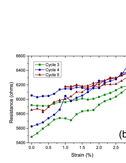
The behavior of the rips determines the electrical transport as a function of strain, as evident in Fig. 4. Figure 4a demonstrates three important features of the data: first, during the initial application of strain (A to B in the Figure) the resistance increases (for this sample, by approximately 43 percent). Typical values for this initial increase in other devices ranged from 20 to 40 percent of the starting resistance. Second, the resistance of the device decreases as the applied strain is relaxed (from B to C) by 7 percent for this device, and typically by between 6 and 14 percent. Finally, in subsequent strain-relaxation cycles over the same strain range the resistance changes only moderately, and in a largely reversible fashion.
The transport behavior can be explained by the opening and closing of rips: in the unstrained device, small rips largely determine the initial resistivity. The device’s resistance increases when the substrate is mechanically stretched, due to the widening of existing rips and formation of new ones; subsequent strain-relaxation cycles over the same strain range, which re-open and close existing rips, generate largely reversible changes in resistance. This reversibility is demonstrated in Fig. 4b; data from the same device recorded during the third, fourth, and fifth strain-relaxation cycles are shown in green, blue, and red respectively. In each case the resistance changes by 14% for 3% applied strain, and returns to within 8% of its original value. Proceeding to a higher strain range forms new rips, consistent with a jump in resistance when the strain range is increased. This behavior – an increase in resistance with the initial application of tensile strain, followed by moderate and reversible changes in the resistance during subsequent strain-relaxation cycles over the same strain region – persists up to approximately 15% applied strain, at which point the devices become permanently non-conducting.
Previous experimental work has demonstrated reversible transport changes in strained graphene, either by depositing graphene on pre-strained substrates so as to create controlled crumplingZang et al. (2013) and bucklingWang et al. (2011), by patterning complex interconnect geometriesKim et al. (2011); Lee et al. (2010), or by measuring transport across macroscopic graphene filmsKim et al. (2009); Bae et al. (2010). In comparison, this work demonstrates the continuing robustness of device functionality after partial mechanical failure. Such resilience is distinctly atypical for conducting thin films: similar studies performed on tin-doped indium oxide (ITO)Cairns et al. (2000) and zinc oxideFortunato et al. (2002) reported rapid and irreversible device failure after the onset of rip formation. One potential explanation for graphene’s exceptional resilience is its morphological simplicity: as a two-dimensional membrane re-establishing electrical contact between two sides of a rip is as simple as overlaying two sheets of paper, while for typical three-dimensional thin films the process is more similar to fitting two halves of a snapped pencil back together.
IV Conclusion
In summary, we have observed the formation and subsequent evolution of micro-rips in graphene using atomic force microscopy. While an initial application of tensile strain introduces new mechanical defects, successive strain-relaxation cycles over the same strain range elastically open and close the existing rips. Mechanics simulations further reveal the underlying deformation and failure mechanisms of the graphene sample under initial and subsequent cyclic tensile loadings, which agree well with the AFM measurements. This mechanical effect has a corresponding electrical effect: the graphene’s transport properties are degraded by the initial application of strain, but show small, mostly reversible changes during ensuing strain-relaxation cycles. Graphene’s combination of superlative electronic properties and robust functionality after partial mechanical failure is unique among conducting thin films and has promising implications for future device applications.
Acknowledgements
We thank Scott Maclaren (UIUC MRL/CMM) for technical assistance. This work was supported by NSF grants #1069076 and #1129826 (SZ, TL), NSF-CMMI grant #1130364 and NSF-NEB grant #486171 (JHH, STG, WJW, NM), and was carried out in part in the Frederick Seitz Materials Research Laboratory Central Facilities, University of Illinois.
References
- Kim et al. (2009) K. S. Kim, Y. Zhao, H. Jang, S. Y. Lee, J. M. Kim, K. S. Kim, J.-H. Ahn, P. Kim, J.-Y. Choi, and B. H. Hong, Nature 457, 706 (2009).
- Bae et al. (2010) S. Bae, H. Kim, Y. Lee, X. Xu, J.-S. Park, Y. Zheng, J. Balakrishnan, T. Lei, H. R. Kim, Y. I. Song, Y.-J. Kim, K. S. Kim, B. Ozyilmaz, J.-H. Ahn, B. H. Hong, and S. Iijima, Nature nanotechnology 5, 574 (2010).
- Lee et al. (2010) Y. Lee, S. Bae, H. Jang, S. Jang, S.-E. Zhu, S. H. Sim, Y. I. Song, B. H. Hong, and J.-H. Ahn, Nano letters 10, 490 (2010).
- Kim et al. (2011) R.-H. Kim, M.-H. Bae, D. G. Kim, H. Cheng, B. H. Kim, D.-H. Kim, M. Li, J. Wu, F. Du, H.-S. Kim, S. Kim, D. Estrada, S. W. Hong, Y. Huang, E. Pop, and J. A. Rogers, Nano letters 11, 3881 (2011).
- El-Kady et al. (2012) M. F. El-Kady, V. Strong, S. Dubin, and R. B. Kaner, Science 335, 1326 (2012).
- Lee et al. (2011) S.-K. Lee, B. J. Kim, H. Jang, S. C. Yoon, C. Lee, B. H. Hong, J. a. Rogers, J. H. Cho, and J.-H. Ahn, Nano letters 11, 4642 (2011).
- Lee et al. (2008) C. Lee, X. Wei, J. W. Kysar, and J. Hone, Science 321, 385 (2008).
- Kim et al. (2012) K. Kim, V. I. Artyukhov, W. Regan, Y. Liu, M. F. Crommie, B. I. Yakobson, and A. Zettl, Nano letters 12, 293 (2012).
- Sen et al. (2010) D. Sen, K. S. Novoselov, P. M. Reis, and M. J. Buehler, Small 6, 1108 (2010).
- Cairns et al. (2000) D. R. Cairns, R. P. Witte, D. K. Sparacin, S. M. Sachsman, D. C. Paine, G. P. Crawford, and R. R. Newton, Applied Physics Letters 76, 1425 (2000).
- Fortunato et al. (2002) E. Fortunato, P. Nunes, A. Marques, D. Costa, H. Águas, I. Ferreira, M. Costa, M. Godinho, P. Almeida, J. Borges, and R. Martins, Advanced Engineering Materials 4, 610 (2002).
- Li et al. (2009) X. Li, W. Cai, J. An, S. Kim, J. Nah, D. Yang, R. Piner, A. Velamakanni, I. Jung, E. Tutuc, S. K. Banerjee, L. Colombo, and R. S. Ruoff, Science 324, 1312 (2009).
- Ferrari et al. (2006) a. C. Ferrari, J. C. Meyer, V. Scardaci, C. Casiraghi, M. Lazzeri, F. Mauri, S. Piscanec, D. Jiang, K. S. Novoselov, S. Roth, and a. K. Geim, Physical Review Letters 97, 187401 (2006).
- Lee et al. (2013) G.-H. Lee, R. C. Cooper, S. J. An, S. Lee, A. van der Zande, N. Petrone, A. G. Hammerberg, C. Lee, B. Crawford, W. Oliver, J. W. Kysar, and J. Hone, Science 340, 1073 (2013).
- Zhu, Huang, and Li (2014) S. Zhu, Y. Huang, and T. Li, Applied Physics Letters 104, 173103 (2014).
- Scharfenberg et al. (2011) S. Scharfenberg, D. Z. Rocklin, C. Chialvo, R. L. Weaver, P. M. Goldbart, and N. Mason, Applied Physics Letters 98, 091908 (2011).
- Zhu and Li (2014) S. Zhu and T. Li, Journal of Applied Mechanics 81, 061008 (2014).
- Zang et al. (2013) J. Zang, S. Ryu, N. Pugno, Q. Wang, Q. Tu, M. J. Buehler, and X. Zhao, Nature materials 12, 321 (2013).
- Wang et al. (2011) Y. Wang, R. Yang, Z. Shi, L. Zhang, D. Shi, E. Wang, and G. Zhang, ACS nano 5, 3645 (2011).