Electronic band structure and ambipolar electrical properties of Cu2O based semiconductor alloys
Abstract
Tuning the opto-electronic properties through alloying is essential for semiconductor technology. Currently, mostly isovalent and isostructural alloys are used (e.g., group-IV and III-V), but a vast and unexplored space of novel functional materials is conceivable when considering more complex alloys by mixing aliovalent and heterostructural constituents. The real challenge lies in the quantitative property prediction for such complex alloys to guide their experimental exploration. We developed an approach to predict compositional dependence of both band-structure and electrical properties from ab-initio calculations by extending conventional dilute defect model to higher (alloy) concentrations. Considering alloying of aliovalent (Mg, Zn, Cd) cations and isovalent anions (S, Se) into Cu2O, we predict tunability of band-gap energies and doping levels over a wide range, including the type conversion from p- to n-type. Initial synthesis and characterization of Zn and Se substituted Cu2O support the defect model, suggesting these alloys as promising novel oxide semiconductor materials.
Introduction
Semiconductor alloys are typically mixtures of two isovalent and isostructural materials, e.g. Si1-xGex in microelectronics Brunner (2002); d’Avezac et al. (2012), Ga1-xInxN for blue light-emitting diodes Nakamura et al. (1995), or Cd1-xZnxTe for radiation detectors Knoll (1999). In photovoltaics, the solar cells with the highest conversion efficiencies above 40 % are multijunction devices with many layers of carefully engineered III-V alloys grown on a Ge substrate Kinsey (2010). Whereas isovalent alloying typically employs compositions from a few per cent up to equal amounts of the constituents, so to modify the band-structure and optical properties, non-isovalent impurity doping Woodyard (1950) is used to tailor the electrical properties via more dilute substitutions ranging from parts per million (1016cm-3) up to few per cent in transparent conducting oxides Ginley and in (2010).
Accordingly, standard theoretical approaches of electronic structure calculations usually address either the modification of band-structure properties due to alloying Lindsay and O’Reilly (1999); Kent and Zunger (2001); Popescu and Zunger (2010) or the manipulation of electrical properties due to doping Northrup and Zhang (1993); Lany and Zunger (2010); Varley et al. (2010). However, a more general approach to semiconductor alloys includes the possibility of mixing aliovalent and heterostructural materials. In this case, the variation of band-structure and electrical properties is inherently coupled, and methods for describing alloy formation enthalpies need to include the Fermi energy as an additional variable that affects the formation enthalpy of non-isovalent substituents and eventually determines the carrier (electron or hole) concentrations in the alloy. A notable previous work in this regard is the study of Sm-doped CeO2 by van de Walle and Ellis van de Walle and Ellis (2007), where the valence mismatch between Ce+IV and Sm+III is accommodated by formation of charged oxygen vacancy defects (V), but without the generation of free carriers.
We approach the aliovalent alloy problem by extending the conventional dilute impurity model to higher (alloy) concentrations and study aliovalent alloying of divalent cations (II = Mg, Zn, Cd) and isovalent chalcogenide anions (VI = S, Se) into a Cu2O matrix. Specifically, we first calculate the formation energies of substitutional dopants and intrinsic defects in the dilute limit. Second, we determine the structures and binding energies of dopant-defect pairs and complexes. Third, knowing the energetically favorable defect structure, we determine the compositional dependence of the band-gap and band-edge energies, which affect the defect formation energies. Finally, based on this input data, we perform thermodynamic simulations for the net doping concentrations as a function of the alloy composition. The results of these simulation are shown in Fig. 1, and we will describe the individual steps in detail below.
The Cu2O parent compound has received considerable interest as one of the few prototypical -type oxides Raebiger et al. (2007a); Scanlon et al. (2009); Nolan and Elliott (2008), and the understanding of the band-structure and defect physics in Cu2O is central to succeed in the quest for the so far elusive p-type transparent conductive oxides Kawazoe et al. (1997); Hautier et al. (2013). The p-type nature of Cu2O has further spurred interest in the areas of magnetic semiconductor Kale et al. (2003); Raebiger et al. (2007b) and in regard of possible applications in photovoltaics Mittiga et al. (2006); Meyer et al. (2012) and photoelectrocatalysis Paracchino et al. (2011). However, as in case of the traditional semiconductor alloys, the controlled tailoring of the band-structure and electrical properties will be instrumental in realizing novel Cu2O based technologies. In particular, ambipolar dopability would open a range of potential applications from oxide electronics to solar energy generation.
Approach and results
In order to theoretically predict both band-structure properties and electrical doping as a function of the alloy composition, we start from the conventional defect theory and supercell formalism de Walle and Neugebauer (2004); Lany and Zunger (2007, 2008); Agoston et al. (2010) and then formulate an approach to extend the dilute impurity model to the higher concentrations present in alloys. Within the standard dilute defect model, the formation energy of a defect in a charge state is defined as
| (1) |
and is a function of two types of variables: (i) , measuring the Fermi energy relative to the valence band maximum (VBM) of the host system and (ii) a set of chemical potentials describing chemical reservoirs. and in eq. (1) are the total energies of a system with and without the defect, respectively. The are defined relative to chemical potentials of the pure elements in their reference phases and reflect the thermodynamic boundary conditions, ranging between Cu-poor / O-rich (CuO/Cu2O coexistence) to Cu-rich / O-poor (Cu/Cu2O). For an accurate prediction of the defect formation energies, we use a recently introduced and tested approach Peng et al. (2013) that combines supercell calculation using density functional theory (DFT) with band-gap corrections from GW quasi-particle energy calculations. Further details of our computational approach are given in the Methods section.
With an increasing concentration of dopants beyond the dilute limit, two effects become more prominent: First, the interaction between dopants and defects can lead to the formation of pairs and larger complexes. Thus, we calculate the different configurations of dopant-defect pairs and their binding energies, and take into account their association and dissociation within the thermodynamic modeling, using the law of mass action Biswas and Lany (2009). Second, since the band-structure changes with the chemical composition, we need to take into account the composition dependence of the individual band edge energies ( and ), which control the formation energies of ionized (charged) defects and dopants (cf. eq. (1)).
Energetics of point defects and defect pairs
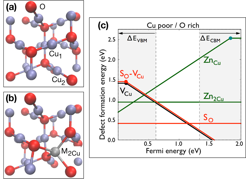
In order to develop a complete defect model for the underlying cuprite structure of Cu2O, we consider the intrinsic defects, i.e. the cation and anion vacancies and interstitials, the extrinsic cation and anion substitutions, as well as defect pairs and complexes between the low-energy species, up to three constituents. Fig. 2(c) shows the defect formation energies of the most relevant point defects and defect pairs, as a function of the Fermi energy at the Cu-poor/O-rich conditions and for the particular II=Zn and VI=S choice. The chemical potential of Zn is limited by the formation of ZnO. The other considered cases of II=Mg,Cd and VI=Se present a qualitatively similar picture. The full list of calculated formation energies is given in the Appendix I. The shaded areas denote the band edge shifts EVBM and ECBM determined from GW calculations. Since oxygen vacancies stay in the electrically inactive neutral charge state irrespective of the Fermi level Raebiger et al. (2007a) and do not show strong binding to other defects, we will not further discuss them.
ZnCu is an electrically active donor-type defect (divalent Zn substituting for monovalent Cu) that assumes a positively charged state for most Fermi energies, and which has a shallow donor level about 0.18 eV below the conduction band minimum. The positively charged Zn attracts negatively charged V resulting in the formation of the electrically neutral Zn2Cu defect complex in which Zn substitutes for two Cu atoms and occupies an interstitial site that is four-fold coordinated by oxygen as shown in Fig. 2(b). This configuration is akin to the Cu vacancy in the ”split vacancy” configuration (one interstitial Cu replaces two lattice Cu atoms), which is a metastable configuration about 0.3 eV higher in energy than the vacancy at the Cu lattice site Wright and Nelson (2002); Raebiger et al. (2007a). Here, however, the Zn2Cu configuration is the ground state, which accommodates the preferential tetrahedral coordination of Zn inside the cuprite lattice, and lies about 1.29 eV lower in energy than the (Zn-V) pair. Analogous defect complexes are formed by the other group II elements Mg and Cd. Further, also the isovalent SO and SeO defects bind Cu vacancies, which can be understood as resulting from compensation of the tensile (SO and SeO) and compressive strain (VCu) induced by the defects. The binding energies relative to the isolated dopants and defects are given in Table 1.
| Defect reaction | Binding energy (eV) |
|---|---|
| Mg + V Mg2Cu | -2.13 |
| Zn + V Zn2Cu | -1.29 |
| Cd + V Cd2Cu | -1.24 |
| SO + V (SO-VCu)- | -0.37 |
| SeO + V (SeO-VCu)- | -0.72 |
Composition dependence of the band-edge energies
In addition to defect-pairing, a second effect that needs to be taken into account when extending the dilute defect model to larger concentrations is the composition dependence of the band-edge energies. Similar as the GW quasiparticle energy shifts (see Fig. 2(c)), the charged defect formation energies vary with a change of the VBM and CBM energies with composition. The band gap and band edge shifts in a Cu2-2x(II)xO1-y(VI)y alloy can then be expressed by a linear expansion ,
| (2) |
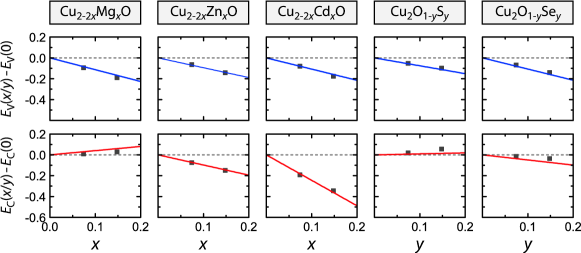
and similar expressions with and for the individual bend edges. The parameters, determined from GW calculations in supercells containing (II)2Cu and (IV)O substitutions are given in Table 2. We note that none of the (II) and (VI) dopants introduce resonant states close to the band edge energies, which could cause large bowing effects, like, e.g. in N doped GaAs Perkins et al. (1999). Thus, the linear expansion, eq. (2), can be expected to be a good approximation within the low to moderate composition range up to considered here. Having the parameters allows predicting directly the defect formation energies of Cu2-2x(II)xO1-y(VI)y alloys using the defect formation energies from the pure Cu2O computed from eq. (1) and the composition dependent band edges from eq. (2). We tested the applicability and accuracy of this approach by performing direct defect calculations on actual alloy compositions as shown in the Appendix III.
| II = Mg | -1.88 | +0.12 | +2.00 |
|---|---|---|---|
| II = Zn | -0.59 | -1.32 | -0.73 |
| II = Cd | -0.97 | -3.26 | -2.30 |
| VI = S | +0.33 | -0.30 | -0.62 |
| VI = Se | +0.06 | -0.88 | -0.95 |
Thermodynamic modeling of defect concentrations and doping
Using the calculated formation energies of point defects and defect pairs, as well as their composition dependence, we performed thermodynamic simulations to determine the concentrations of the substituted elements and the VCu defects. Under equilibrium conditions, the site concentration of a defect , i.e., the concentration of defects divided by that of the lattice sites on which the defect resides, is given approximately by . Due to the Fermi level dependence of in case of electrically active defects or dopants (cf. eq. (1)), needs to be solved together with the defect concentrations, which is achieved by a numerical self-consistent solution under the constraint of overall charge neutrality between charged defects and carriers (free electrons and holes) Lany et al. (2005); Lany and Zunger (2007). In the present work, we further take into account the association and dissociation of defect pairs within the self-consistent solution, as described in Ref. Biswas and Lany (2009). The thermodynamics of the association and dissociation of defect pairs is described by the law of mass action, e.g.
| (3) |
where the brackets denote the site concentrations of the respective species and include the multiplicity of the equivalent configurations of the defect pairs Biswas and Lany (2009). The electrical properties are characterized by the common ”net doping concentration”, i.e., the difference between the total donor and acceptor concentrations. In the following, we apply this model to three situations, (i) the intrinsic doping of pure Cu2O due to VCu formation, (ii) the equilibrium solubility limits of the group II and VI dopants, and (iii) the composition dependence of electrical properties in alloys at non-equilibrium compositions.
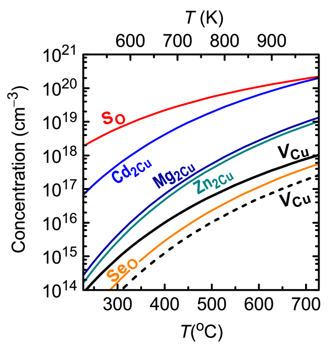
As shown in Fig. 3, we find that in pure Cu2O, the VCu concentration varies between the mid-1015 to mid 1016 cm-3 range between the Cu-rich (Cu2O/Cu) and Cu-poor (Cu2O/CuO) conditions at T = 450∘C, agreeing well with the hole carrier density of about 1015 cm-3 measured in Cu2O sheets quenched from this temperature Mittiga et al. (2006, 2009). In order to determine the solubility limits of the group II and VI dopants, we take into account the constraints to their chemical potentials arising from phase separation and the ensuing precipitation of the competing phases, i.e., MgO, ZnO, CdO, Cu2S, Cu2Se. As seen in Fig.3, the resulting equilibrium solubilities can exceed 1020 cm-3, but remain in the range of dilute doping below the percent range. Since the dominant defect configurations, i.e., the (VI)O substitution and the (II)2Cu pair, are charge neutral (cf. Fig. 2c), and since the effect on the band energies is minute at such low concentrations, the electrical properties do not significantly change compared to pure Cu2O.
The solubility limits of dopants can often be overcome by non-equilibrium techniques, such as low-temperature thin-film growth Desnica (1998); Zakutayev et al. (2012). In fact, the solubility limits are often attained only after prolonged annealing procedures at high temperatures González et al. (2012). Similarly, in alloys where the positive mixing enthalpy creates a ”miscibility gap” in equilibrium, such compositions can nevertheless be realized under synthesis conditions where the long-range diffusion necessary for phase separation is kinetically limited Singh et al. (1997). In case of heterostructural alloys, the lattice mismatch provides a further barrier for nucleation of secondary phases. Thus, we are now addressing the question which range of band-gaps and electrical doping can be achieved in Cu2-2x(II)xO1-y(VI)y if the alloy composition is treated as a parameter that can exceed the thermodynamic solubility limit. To this end, we performed the thermodynamic modeling for a partial equilibrium Lany and Zunger (2009), in which the constraints due to phase separation and precipitation are omitted. In practice, the dopant chemical potential is adjusted during the thermodynamic simulation until the respective alloy composition is attained. This situation corresponds to a supersaturation of dopants, i.e., the dopant chemical potential is higher and the respective defect formation energy is lower than in the unconstrained equilibrium where precipitation of secondary phases (e.g., ZnO, Cu2S, etc.) limits the solubility. The balance between electrically active dopants and the compensating intrinsic defects determines the electrical properties. Such partial equilibrium simulations have recently explained successfully the temperature dependence of the conductivity in Ga doped ZnO Zakutayev et al. (2013a).
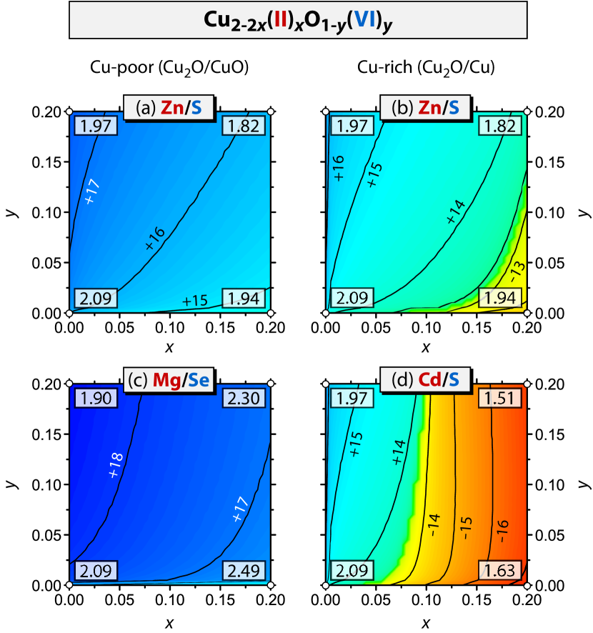
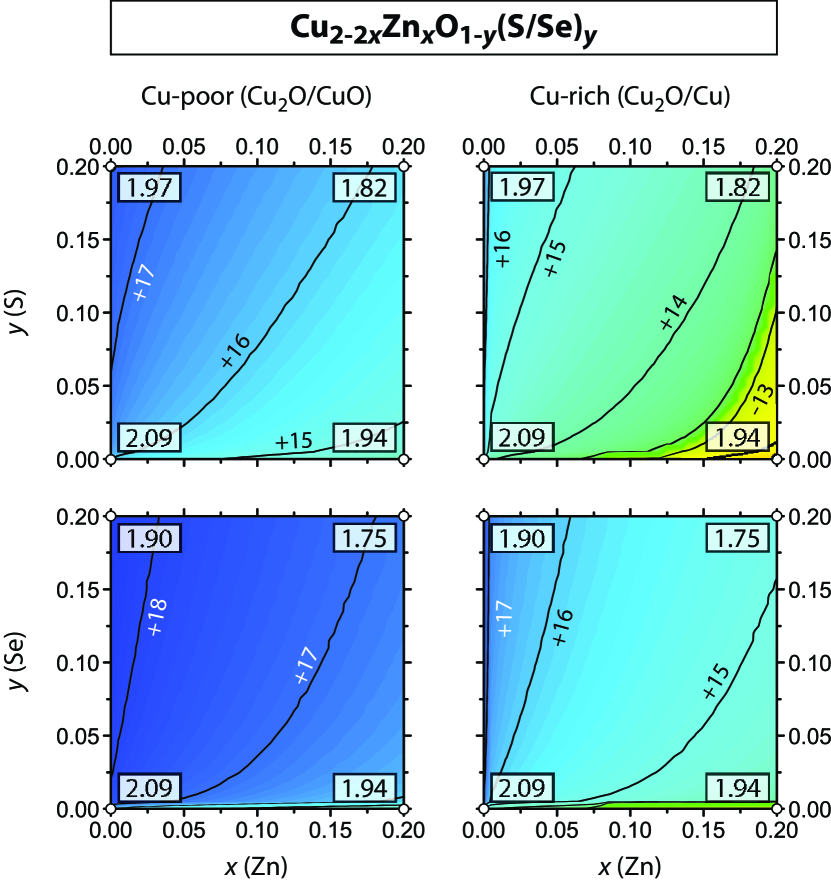
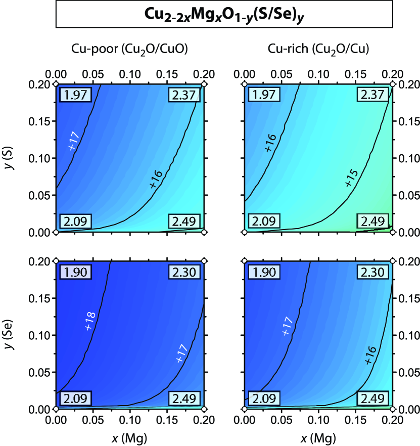
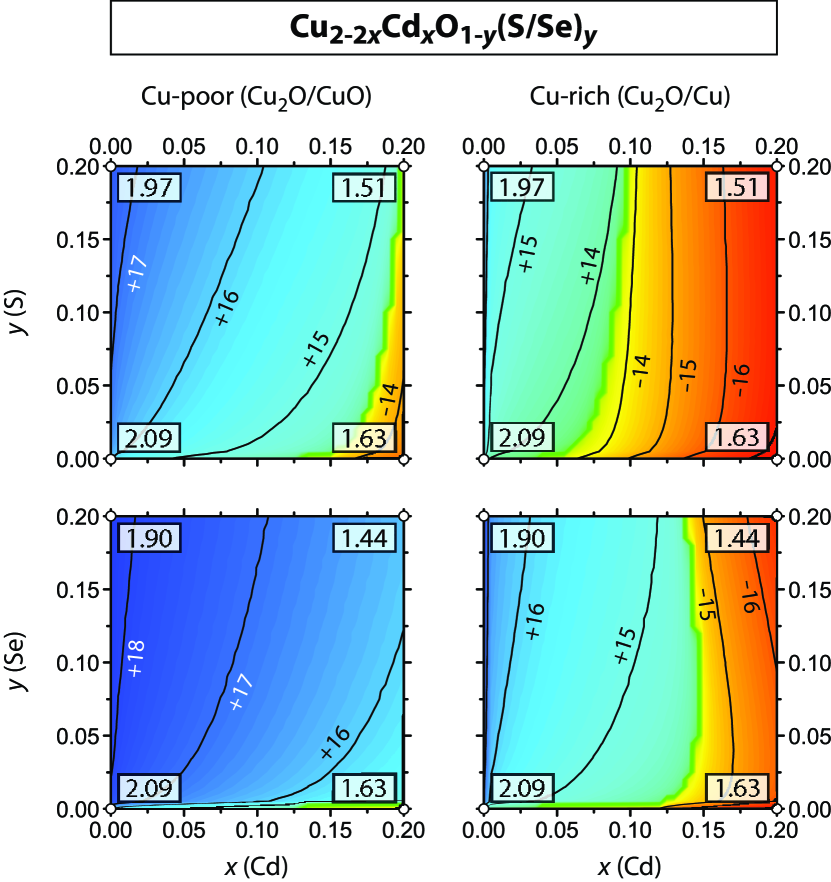
The contour plot in Fig. 1 shows the net-doping in Cu2-2x(II)xO1-y(VI)y alloys as a function of and ( and stand for the concentration of donors and acceptors, respectively). The numbers in the corners give the predicted band gaps for the respective end point compositions according to eq. (2) and the data in Table 2. For the Zn/S combination, we show the net-doping for both Cu poor (equilibrium between Cu2O and CuO) and Cu rich (equilibrium between Cu2O and Cu) conditions, thereby illustrating the dependence on the growth conditions. The combinations Mg/Se and Cd/S are shown for the Cu poor and Cu rich conditions, respectively, thereby emphasizing the most pronounced -type (due to Se) and -type (due to Cd) doping scenarios. Within the composition range , we obtain band gaps between 1.44 eV (for the Cd/Se combination at, not shown in Fig. 1) and 2.49 eV (for Mg alloying at ). The complete data set including all II/VI combinations is given in the Appendix II.
Experimental synthesis
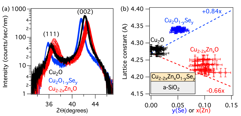
As a first step towards the experimental realization of these novel functional Cu2O alloys, we used an combinatorial synthesis and characterization approach Zakutayev et al. (2013b) to grow thin films of Cu2O, Cu2-2xZnxO, and Cu2O1-ySey Zakutayev et al. (2011),and to characterize these films in spatially resolved way Zakutayev et al. (2012) using X-ray diffraction. Figure 4(a) shows the X-ray diffraction data for pure Cu2O, for varying Zn substitution centered around , and for varying Se substitution centered around . No impurity phases of ZnO or Cu2Se are observed. The measured composition dependence of the lattice constant is compared with the prediction of the defect model in Fig. 4(b). The trend of a reduction of the lattice constant due to Zn alloying and an increase due to Se alloying is observed in both the experimental and theoretical data sets, suggesting that the alloyed elements are incorporated in the cuprite lattice as described by the computational defect model, instead of forming secondary phases. Note that the presence of residual strain in the films leads to a slightly larger lattice constant of Cu2O than in single crystals, where = 4.27 Å, and that the present type of DFT calculations cause a typical, but not exactly systematic overestimation of the lattice constant by about 1 %.
Discussion
The extension of the traditional dilute defect model towards larger alloy concentrations enables the prediction of doping in aliovalent alloys, thereby opening a path to design the electrical properties in complex semiconductor materials. Notably, the electrical behavior of the Cu2-2x(II)xO1-y(VI)y alloys differs markedly from the traditional doping mechanism Woodyard (1950), where aliovalent impurity atoms introduce a number of charge carriers that is comparable to the number dopant atoms (although a certain reduction from unity doping efficiency is often caused by self-compensation Mandel (1964)).
Our model predicts an interesting and counterintuitive doping behavior, in that the aliovalent group-II dopants have a negligible effect on the electrical properties at typical sub-percent doping levels (see Fig. 1), but modify the band gap at higher alloy-like concentrations. On the other hand, the isovalent group-VI substitution has a rather modest effect on the band gap, but increases the hole-carrier concentration significantly. This rather ironic behavior is explained by the important role of dopant-defect interactions in this system: The divalent dopants incorporate dominantly in the form of a valence-conserving defect complex, e.g., Zn2Cu, where one Zn+II replaces two Cu+I ions. This charge-neutral complex is electrically inactive, but it modifies the band structure. As seen in see Table 2, Mg alloying lowers the VBM energy, which can be explained by the fact that Mg lacks an occupied -shell, and therefore reduces the density of states at the Cu- like top of the valence band. Zn and Cd introduce delocalized, unoccupied -like states, which cause a lowering of the CBM energy. The isovalent dopants have a smaller effect on the band structure but affect the electrical properties. The binding energy between substitutional SO or SeO dopants and Cu vacancy VCu effectively reduces the formation enthalpy of these hole-producing defects when forming close to the isovalent dopant, thereby increasing the -type doping with increasing S/Se alloying.
We considered the range as a composition range within which the realization of Cu2-2x(II)xO1-y(VI)y alloys could be achievable by non-equilibrium growth methods. Within this composition window, we obtain predicted band gap energies between 1.4 () and 2.5 eV () from the values given in Table 2, compared to the 2.1 eV room temperature gap of Cu2O Malerba et al. (2011). Whereas the binary oxide Cu2O is always -type conducting within a narrow window Meyer et al. (2012); Mittiga et al. (2009); Papadimitriou (1993) we find the alloying approach allows a much better control of the electrical properties. Due to the pronounced dopant-defect interaction, alloying of S and Se increases the -type doping, up to the range for (Fig. 1). For the case of cation doping, the formation of dopant-defect complexes like Zn2Cu prevents effective -type doping. However, at very high concentrations of Zn or Cd beyond the dilute doping regime, i.e. in the aliovalent alloying regime, we observe type conversion from - to -type with a maximal electron doping level of at (see Fig. 1).
The physical origin of the type conversion from - to -type is a combination of two causes. First, the increased non-equilibrium chemical potential of the group II element effectively lowers the formation energy of the (II)Cu donors, which otherwise is rather high (see Fig. 2(c)). Note that most II elements are still incorporated as charge neutral (II)2Cu defect pairs, and only a fraction forms as a substitutional donor, e.g., CdCu, as determined by the law of mass action (see eq. (3)). In fact, only a fraction of about of alloyed Cd atoms become electrically active as -type dopants. The second effect is the lowering of the CBM energy with the composition for Zn and Cd, which supports -type doping by bringing the CBM closer to the equilibrium Fermi level during the thermodynamic simulation. This effect is most pronounced for Cd alloying which affords the largest reduction of the CBM energy, as seen in the parameter in Table 2, and which is the only group II dopant that can be expected to produce robust -type doping with appreciable carrier densities (Fig. 1).
The synthesis and characterization of Zn and Se substituted Cu2O alloys shows no indication of impurity phases (ZnO or Cu2Se), and the composition dependence of the lattice parameter is consistent with the computational defect model. Thus, the initial experimental data supports the viability of the proposed alloy system.
Conclusions
In conclusion, the band-structure and electrical properties of complex Cu2-2x(II)xO1-y(VI)y alloys were modeled by extending the dilute defect model to finite alloy compositions, taking into account pair and complex formation between of dopants and defects, as well as the composition dependence of the band edge energies. In contrast to conventional semiconductor systems, where the manipulation of band-structure properties via isovalent alloying is separated from the control of electrical properties via dilute aliovalent doping, the two mechanisms become intertwined due to the dopant-defect interactions. Considering the alloying of aliovalent (Mg, Zn, Cd) cations and isovalent anions (S, Se) into Cu2O, we predicted that the band-gap energies and the doping levels are tunable over a wide range (gap from 1.4 to 2.5 eV, carriers from cm-1 to cm-1), including the type conversion from p- to n-type. The initial thin film synthesis and characterization of these novel oxide semiconductor materials has shown a single phase formation beyond the thermodynamic solubility limit, thereby supporting the underlying defect model. The Cu2-2x(II)xO1-y(VI)y alloys could find application, e.g., as alternative earth abundant photovoltaic materials.
Acknowledgements
This work was supported by the US Department of energy, Office of Energy Efficiency and Renewable Energy, under Contract No. DE-AC36-08GO28308 to the National Renewable Energy Laboratory (NREL), as part of a Next Generation Photovoltaics II project within the SunShot initiative. The use of high performance computing resources of the National Energy Research Scientific Computing Center and of NREL’s Computational Science Center are gratefully acknowledged. V.S. also acknowledges the administrative support of REMRSEC at the Colorado School of Mines.
Appendix I: Methods
Theory and modeling: All DFT calculations were performed with the projector augmented-wave (PAW) method Blöchl (1994) as implemented in the VASP code Kresse and Joubert (1999), employing the PBE exchange-correlation functional Perdew et al. (1996), and the DFT+U formulation of Ref. Dudarev et al. (1998), with U = 5 eV for Cu- orbitals. Defects and defect pairs were modeled in large supercells of Cu2O with 162 atoms, applying the standard finite-size corrections for image charge interactions and potential alignment Lany and Zunger (2009). The band gap problem was resolved by combining the DFT supercell energies with the results from GW quasi-particle energy calculations as described in Ref. Peng et al. (2013), using the band edge shifts E eV and E eV, as determined in a recent GW study of transition metal oxides Lany (2013). In oder to accurately describe the chemical potentials entering in eq. (1), we have used the fitted elemental refrence energies (FERE) of Ref. Stevanović et al. (2012). For the host atoms Cu and O, the chemical potentials are limited by the phase coexistence of Cu2O with CuO (Cu-poor/O-rich condition; eV and eV) and with metallic Cu (Cu-rich/O-poor condition; eV and eV). For the thermodynamic solubility limits, the chemical potentials of the extrinsic impurities are determined by the condition of phase coexistence with the related secondary phases, e.g. MgO, ZnO, CdO, Cu2S, Cu2Se. All defect formation energies for the charge neutral defects and defect pairs, given for , are provided in Table 3
To determine the effect of (II)2Cu and (VI)O substitution on band-edge energies, we performed direct GW calculations in 48 atom supercells containing one of these defects. These GW calculations were performed analogously to those in Ref. Lany (2013) using the implementation of the GW method in the PAW framework Ref. Shishkin and Kresse (2006).
We note that GW calculations are generally difficult to converge Samsonidze et al. (2011); Friedrich et al. (2011). For the PAW implementation of the GW method, a recent work Klimeš et al. has identified limitations due to basis set incompleteness, which are particularly pronounced for d-orbitals. We think it is likely that these issues lie behind the previously observed need to apply an external d-state potential in GW for transition metal compounds Lany (2013). Including these potentials (here, Vd = -2.4, -1.5, and -0.5 eV for Cu, Zn, and Cd, respectively) mitigates these issues, and should lead to fairly reliable valence band shifts, as indicated by the good agreement of the calculated ionization potentials with experimental data Stevanović et al. (2014).
We further performed a test of the underlying assumption of our model that the charged defect formation enthalpies vary linearly with the change of the VBM energy (cf. eqs. (1) and (2)). To this end, we performed defect calculations in explicit alloy supercells using the same 162 atom Cu2O cells as above, sampling over different alloy compositions (4 and 8 cation or anion substitutions), alloy configurations and different defect sites in each representation. Since GW calculations for such large supercells are not feasible, this test was performed on the DFT+U level. Further details are provided in Supplementary materials.
In order to calculate the doping and defect concentrations, we use a thermodynamic model Lany and Zunger (2007); Biswas and Lany (2009); Lany et al. (2005), where a self-consistency condition is solved numerically for the formation energy , the defect concentration, and the Fermi level under the constraint of overall charge neutrality. The case of the partial equilibrium is solved by adjusting the defect formation energy for atomic substitution during the simulation until the respective alloy concentration is obtained. The temperature dependence of the Cu2O band gap, as determined in Ref. Iwamitsu et al. (2012) was taken into account in the thermodynamic simulation. The calculated carrier densities in pure Cu2O are in agreement with available experimental data Mittiga et al. (2006, 2009), but about 2 orders of magnitude lower than those determined before in Ref. Raebiger et al. (2007a). This difference results mostly from the GW quasi-particle energy shift of the VBM, which increases H(V) by 0.62 eV relative to a standard DFT+U calculation.
The case of the partial equilibrium is solved by adjusting the defect formation energy for atomic substitution during the simulation until the respective alloy concentration is obtained.
Thin-film deposition: Thin films of Cu2O, Cu2-2xZnxO, and Cu2O1-ySey were grown at ambient temperature by combinatorial RF co-sputtering with a continuous composition spread Zakutayev et al. (2011) in a AJA International vacuum chamber with 10-10 atm base pressure, and filled with 10-6 atm of ultra high purity Ar. We used 50x50 mm Eagle-XG glass substrates and 50 mm diameter targets of Cu2O, ZnO and Cu2Se. The films were characterized at 44 spatially distinct locations Zakutayev et al. (2012), determining the composition and thickness (350-650 nm range) by x-ray fluorescence (XRF), and determining the phase composition and lattice constant by X-ray diffraction (XRD).
| [eV] | [eV] | ||
|---|---|---|---|
| VCu | (A) | +1.65 | 0.13 |
| MgCu | (D) | -1.32 | 0.17 |
| ZnCu | (D) | +0.59 | 0.18 |
| CdCu | (D) | +1.17 | 0.18 |
| VO | +2.42 | - | |
| SO | +1.27 | - | |
| SeO | +2.14 | - | |
| Mg2Cu | -3.52 | - | |
| Zn2Cu | -0.76 | - | |
| Cd2Cu | -0.13 | - | |
| (SO-VCu) | (A) | +2.55 | 0.13 |
| (SeO-VCu) | (A) | +3.07 | 0.13 |
Appendix II: Complete data of thermodynamic modeling
Appendix III: Test of alloy model
The present work utilizes a model to determine to linear order the composition-dependence of the band gap and the individual band edge energies. We here test this linear extrapolation by comparison with calculations of supercells that explicitly incorporate different alloy compositions. Specifically, we are using 162 atom supercells containing 4 and 8 cation or anion substitutions, e.g., Zn2Cu or SO with or = 0.074 and 0.148. In all cases, the results of two different random alloy representations were averaged. Since GW calculations for such large supercells are not feasible, we conduct the test of the model on the GGA+U level. The actual results take also into account that the GW quasi-particle energy shifts vary with composition, thereby giving rise to a GW contribution to the composition dependence.
| (GGA+U) | (GGA+U) | (GW) | (GW) | |
|---|---|---|---|---|
| Mg2Cu | -1.13 | +0.40 | -0.75 | -0.28 |
| Zn2Cu | -0.94 | -0.97 | +0.36 | -0.35 |
| Cd2Cu | -1.08 | -2.44 | +0.11 | -0.82 |
| SO | -0.76 | +0.09 | +1.09 | -0.39 |
| SeO | -1.07 | -0.49 | +1.13 | -0.39 |
.1 Composition dependence of the band edge energies
In semiconductor alloys, the composition dependence of the band gap and of the band edge energies is usually described up to quadratic order via a bowing parameter. However, in the composition window , considered in the present work, this dependence is approximately linear. We determined the composition dependence of , , and (see Table 2) by calculating a single substitution in a 48-atom supercell, both in GGA+U and in GW. The individual contributions are given in Table 4. Potential alignment effects have been taken into account to determine the energy lineup between pure and substituted Cu2O supercells, using all atoms except the substituted ones as references. The change of the crystal volume with composition was taken into account in both the linear extrapolation model and the explicit alloy supercell calculations. Figure 8 shows that both approaches agree very well on the predicted composition dependence of the individual band edge energies (and, hence, on the predicted band gap). We note that a deviation from the linear proportionality would be expected in case of substitutions that cause defect states inside the band gap, which would create a discontinuity of the band edge energies at . This behavior is not observed for the alloy substitutions considered in the present work.
.2 Composition dependence of the charged-defect formation energies
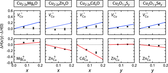
In order to extend the dilute defect model to low and moderate alloy compositions, we consider two effects that affect the defect concentrations. First, the effect of defect pair association is taken into account by calculating the binding energy and using the law of mass action. Second, the linear extrapolation of the band edge energies leads to a composition dependence of the charged defect () formation energy via eq. (1). We test this model by comparison with defect formation energy calculations in the explicit alloy supercells, averaging over five different defect sites in each of the two alloy representations. Here, we exclude the Cu sites next to the anion (S or SeO) dopants, because the treatment of the pair association already accounts for the lowering of the VCu formation energy at these sites. Showing the comparison between the extrapolation model and the explicit ally supercell defect calculations, we see in Fig. 9 that for all cases except VCu in the cation-substituted case the model captures well the trends in the composition dependence of and gives reasonable quantitative estimates. In the cation substituted cases, calculated in the alloy supercells is lower than the value expected from the extrapolation model. This observation can be explained by the fact that that there is a binding energy of, e.g., -0.20 eV between the Zn2Cu substitution and VCu at the Cu site nearest to the Zn location. In principle, one can refine the treatment of the pair and complex association to include larger clusters and more configurations with their individual binding energies, e.g., by including a (Zn2Cu-VCu) complex. However, in practice, one has to cut off the defect interactions at some point, and we feel that the purpose of the present work is better served by including for clarity only the leading mechanisms for defect pair formation that are shown in Table 1. To conclude, the test using explicit alloy supercells has confirmed that the defect pair association and the shift of the band edge energies are the leading effects that need to be included to predict defect formation beyond the dilute limit in low and moderate alloy compositions.
References
- Brunner (2002) K. Brunner, Rep. Prog. Phys. 65, 27 (2002).
- d’Avezac et al. (2012) M. d’Avezac, J.-W. Luo, T. Chanier, and A. Zunger, Phys. Rev. Lett. 108, 027401 (2012).
- Nakamura et al. (1995) S. Nakamura, M. Senoh, N. Iwasa, and S. Nagahama, Jpn. J. Appl. Phys. 34, L797 (1995).
- Knoll (1999) G. F. Knoll, Radiation Detection and Measurement, 3rd ed. (Wiley, New York, USA, 1999).
- Kinsey (2010) G. Kinsey, High-Concentration, III–V Multijunction Solar Cells in Solar cells and their applications (Wiley, New York, 2010).
- Woodyard (1950) J. Woodyard, U.S. Patent No. 2,530,110 (1950).
- Ginley and in (2010) D. S. Ginley and J. D. P. in, ”Handbook of Transparent Conductors”, D. S. Ginley, H. Hosono, and D. C. Payne (Springer, New York, 2010).
- Lindsay and O’Reilly (1999) A. Lindsay and E. O’Reilly, Solid State Commun. 112, 443 (1999).
- Kent and Zunger (2001) P. R. C. Kent and A. Zunger, Phys. Rev. B 64, 115208 (2001).
- Popescu and Zunger (2010) V. Popescu and A. Zunger, Phys. Rev. Lett. 104, 236403 (2010).
- Northrup and Zhang (1993) J. E. Northrup and S. B. Zhang, Phys. Rev. B 47, 6791 (1993).
- Lany and Zunger (2010) S. Lany and A. Zunger, Appl. Phys. Lett. 96, 142114 (2010).
- Varley et al. (2010) J. B. Varley, A. Janotti, and C. G. V. de Walle, Phys. Rev. B 81, 245216 (2010).
- van de Walle and Ellis (2007) A. van de Walle and D. E. Ellis, Phys. Rev. Lett. 98, 266101 (2007).
- Raebiger et al. (2007a) H. Raebiger, S. Lany, and A. Zunger, Phys. Rev. B 76, 045209 (2007a).
- Scanlon et al. (2009) D. O. Scanlon, B. J. Morgan, G. W. Watson, and A. Walsh, Phys. Rev. Lett. 103, 096405 (2009).
- Nolan and Elliott (2008) M. Nolan and S. D. Elliott, Chem. Mater. 20, 5522 (2008).
- Kawazoe et al. (1997) H. Kawazoe, M. Yasukawa, H. Hyodo, M. Kurita, H. Yanagi, and H. Hosono, Nature 389, 939 (1997).
- Hautier et al. (2013) G. Hautier, A. Miglio, G. Ceder, G.-M. Rignanese, and X. Gonze, Nat. Commun. 4, 2292 (2013).
- Kale et al. (2003) S. N. Kale, S. B. Ogale, S. R. Shinde, M. Sahasrabuddhe, V. N. Kulkarni, R. L. Greene, and T. Venkatesan, Appl. Phys. Lett. 82, 2100 (2003).
- Raebiger et al. (2007b) H. Raebiger, S. Lany, and A. Zunger, Phys. Rev. Lett. 99, 167203 (2007b).
- Mittiga et al. (2006) A. Mittiga, E. Salza, F. Sarto, M. Tucci, and R. Vasanthi, Appl. Phys. Lett. 88, 163502 (2006).
- Meyer et al. (2012) B. K. Meyer, A. Polity, D. Reppin, M. Becker, P. Hering, P. J. Klar, T. Sander, C. Reindl, J. Benz, M. Eickhoff, C. Heiliger, M. Heinemann, J. Bläsing, A. Krost, S. Shokovets, C. Müller, and C. Ronning, Phys. Status Solidi B 249, 1487 (2012).
- Paracchino et al. (2011) A. Paracchino, V. Laporte, K. Sivula, M. Graetzel, and E. Thimsen, Nature Materials 10, 456 (2011).
- de Walle and Neugebauer (2004) C. G. V. de Walle and J. Neugebauer, J. Appl. Phys. 95, 3851 (2004).
- Lany and Zunger (2007) S. Lany and A. Zunger, Phys. Rev. Lett. 98, 045501 (2007).
- Lany and Zunger (2008) S. Lany and A. Zunger, Phys. Rev. B 78, 235104 (2008).
- Agoston et al. (2010) P. Agoston, C. Körber, A. Klein, M. J. Puska, R. M. Nieminen, and K. Albe, J. Appl. Phys. 108, 053511 (2010).
- Peng et al. (2013) H. Peng, D. O. Scanlon, V. Stevanovic, J. Vidal, G. W. Watson, and S. Lany, Phys. Rev. B 88, 115201 (2013).
- Biswas and Lany (2009) K. Biswas and S. Lany, Phys. Rev. B 80, 115206 (2009).
- Wright and Nelson (2002) A. F. Wright and J. S. Nelson, J. Appl. Phys. 92, 5849 (2002).
- Perkins et al. (1999) J. D. Perkins, A. Mascarenhas, Y. Zhang, J. Geisz, D. Friedman, J. Olson, and S. Kurtz, Phys. Rev. Lett. 82, 3312 (1999).
- Lany et al. (2005) S. Lany, Y.-J. Zhao, C. Persson, and A. Zunger, Appl. Phys. Lett. 86, 042109 (2005).
- Mittiga et al. (2009) A. Mittiga, F. Biccari, and C. Malerba, Thin Solid Films 517, 2469 (2009).
- Desnica (1998) U. V. Desnica, Progress in Crystal Growth and Characterization of Materials 36, 291 (1998).
- Zakutayev et al. (2012) A. Zakutayev, T. R. Paudel, P. F. Ndione, J. D. Perkins, S. Lany, A. Zunger, and D. Ginley, Phys. Rev. B 85, 085204 (2012).
- González et al. (2012) G. B. González, T. O. Mason, J. S. Okasinski, T. Buslaps, and V. Honkimäki, J. Am. Ceram. Soc. 95, 809 (2012).
- Singh et al. (1997) R. Singh, D. Doppalapudi, T. D. Moustakas, and L. T. Romano, Appl. Phys. Lett. 70, 1089 (1997).
- Lany and Zunger (2009) S. Lany and A. Zunger, Modelling Simul. Sci. Eng. 17, 084002 (2009).
- Zakutayev et al. (2013a) A. Zakutayev, N. H. Perry, T. O. Mason, D. S. Ginley, and S. Lany, Appl. Phys. Lett. 103, 232106 (2013a).
- Zakutayev et al. (2013b) A. Zakutayev, F. J. Luciano, V. P. Bollinger, A. K. Sigdel, P. F. Ndione, J. D. Perkins, J. J. Berry, P. A. Parilla, and D. S. Ginley, Rev. Sci. Instr. 84, 053905 (2013b).
- Zakutayev et al. (2011) A. Zakutayev, J. D. Perkins, P. A. Parilla, N. E. Widjonarko, A. K. Sigdel, J. J. Berry, and D. Ginley, MRS Communications 1, 23 (2011).
- Mandel (1964) G. Mandel, Phys. Rev. 134, A1073 (1964).
- Malerba et al. (2011) C. Malerba, F. Biccari, C. L. A. Ricardo, M. D Incau, P. Scardi, and A. Mittiga, Sol. En. Mater. Sol. Cells 95, 2848 (2011).
- Papadimitriou (1993) L. Papadimitriou, Solid-State Electron. 36, 431 (1993).
- Blöchl (1994) P. E. Blöchl, Phys. Rev. B 50, 17953 (1994).
- Kresse and Joubert (1999) G. Kresse and D. Joubert, Phys. Rev. B 59, 1758 (1999).
- Perdew et al. (1996) J. P. Perdew, K. Burke, and M. Ernzerhof, Phys. Rev. Lett. 77, 3865 (1996).
- Dudarev et al. (1998) S. L. Dudarev, G. A. Botton, S. Y. Savrasov, C. J. Humphreys, and A. P. Sutton, Phys. Rev. B 57, 1505 (1998).
- Lany (2013) S. Lany, Phys. Rev. B 87, 085112 (2013).
- Stevanović et al. (2012) V. Stevanović, S. Lany, X. Zhang, and A. Zunger, Phys. Rev. B 85, 115104 (2012).
- Shishkin and Kresse (2006) M. Shishkin and G. Kresse, Phys. Rev. B 74, 035101 (2006).
- Samsonidze et al. (2011) G. Samsonidze, M. Jain, J. Deslippe, M. L. Cohen, and S. G. Louie, Phys. Rev. Lett. 107, 186404 (2011).
- Friedrich et al. (2011) C. Friedrich, M. C. Müller, and S. Blügel, Phys. Rev. B 83, 081101(R) (2011).
- (55) J. Klimeš, M. Kaltak, and G. Kresse, arXiv:1404.3101 .
- Stevanović et al. (2014) V. Stevanović, S. Lany, D. S. Ginley, W. Tumas, and A. Zunger, Phys. Chem. Chem. Phys. 16, 3706 (2014).
- Iwamitsu et al. (2012) K. Iwamitsu, S. Aihara, T. Shimamoto, A. Fujii, and I. Akai, physica status solidi (c) 9, 1610 (2012).