Raman spectroscopy as probe of nanometer-scale strain variations in graphene
Abstract
Confocal Raman spectroscopy is a versatile, non-invasive investigation tool and a major workhorse for graphene characterization. Here we show that the experimentally observed Raman 2D line width is a measure of nanometer-scale strain variations in graphene. By investigating the relation between the G and 2D line at high magnetic fields we find that the 2D line width contains valuable information on nanometer-scale flatness and lattice deformations of graphene, making it a good quantity for classifying the structural quality of graphene even at zero magnetic field.
Graphene combines several highly interesting material properties in a unique way, promising unprecedented material functionalities. This makes graphene increasingly attractive for industrial applications Novoselov et al. (2012) but, at the same time, stresses the need for non-invasive characterization techniques. In recent years, Raman spectroscopy has proven to be highly useful as a non-invasive method not only to identify graphene Ferrari et al. (2006); Graf et al. (2007), but also to extract information on local doping Ferrari (2007); Yan et al. (2007); Pisana et al. (2007); Stampfer et al. (2007), strain Mohr et al. (2010); Huang et al. (2010) and lattice temperature Calizo et al. (2007); Balandin et al. (2008). Even more insights can be gained when utilizing confocal, scanning Raman spectroscopy to study spatially resolved doping domains Stampfer et al. (2007); drogeler2014, edge effects casiraghi2009; Graf et al. (2007) and position dependent mechanical lattice deformations, including strain mohiuddin2009; zabel2012; yoon2011a. The spatial resolution of so-called Raman maps is on the order of the laser spot size (which for confocal systems is typically on the order of 500 nm) and the extracted quantities (such as doping or strain) are in general averaged over the spot size. It is therefore important to distinguish between length scales significantly larger or smaller than the laser spot size. In particular, we will distinguish between strain variations on a micrometer scale, which can be extracted from spatially resolved Raman maps, and nanometer-scale strain variations, which are on sub-spot-size length scales and cannot be directly observed by Raman imaging, but are considered as important sources of scattering for electronic transport couto2014.
Here we show that the experimentally observed Raman 2D line width is a measure of nanometer-scale strain variations in graphene on insulating substrates, i.e. it contains valuable information on local (i.e. nanometer-scale) flatness, lattice deformations and crystal quality of graphene. To prove that the the experimentally observed 2D line width depends on sub-spot size strain variations and lattice deformations we employ the following strategy:
(i) We start by showing that by combining Raman spectroscopy with magnetic fields, electronic broadening contributions for the Raman G line width can be strongly suppressed. Since in perpendicular magnetic fields the electronic states in graphene condense into Landau levels (LLs), the interaction between electronic excitations and lattice vibrations becomes field dependent. In agreement with existing theory ando2007; goerbig2007; kashuba2012; qiu2013 and experiments yan2010; neumann2015, we demonstrate that by applying a perpendicular field of around 8 T, the G line does as good as not depend on electronic properties such as charge carrier doping, screening or electronic broadening.
(ii) We observe that, under these conditions, the G line width nevertheless exhibits strong variations across graphene flakes. In particular, we show that the G line width is significantly increased in regions where the graphene flake features bubbles and folds, i.e. in correspondence with increased structural deformations.
(iii) Finally, we show that at 8 T there is a (nearly) linear dependence between the G line width and the 2D line width, implying that there is a common source of line broadening. According to points (i) and (ii) the broadening must be related to structural lattice deformations. This finding is further supported by a detailed analysis of the relation between the area of the 2D peak and its line width. By analyzing the relation between the G and 2D line width, we find that nm-scale strain variations constitute a dominant contribution to the observed line broadenings. Importantly, the 2D line has been shown to be only very weakly dependent on the field Faugeras2010, meaning that no magnetic field is required to extract information on nm-scale strain variations from the 2D line width, which makes this quantity interesting for practical applications.

For the low temperature Raman measurements, we employ a commercially available confocal Raman setup that allows us to perform spatially-resolved experiments at a temperature of 4.2 K and magnetic fields of up to 9 T. We use an excitation laser wavelength of 532 nm with a spot diameter on the sample of around 500 nm. For detection, we use a single mode optical fiber and a CCD spectrometer with a grating of 1200 lines/mm. All measurements are performed with linear laser polarization and a 100 objective.
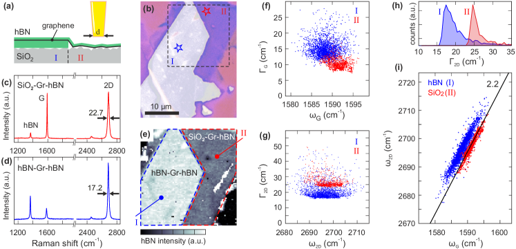
The investigated graphene (Gr) sheet is partly encapsulated in hexagonal boron nitride (hBN) and partly sandwiched between SiO2 and hBN as illustrated in Figure 1a. An optical image of our sample is shown in Figure 1b. In contrast to graphene encapsulated in hBN, graphene flakes supported by SiO2 usually feature lower carrier mobilities of around - cm2/(Vs), indicating a detrimental influence of SiO2 on the electronic properties of graphene. In this regard, our structure gives us the invaluable capability of probing a single graphene sheet exposed to two different substrates (region I and II in Figures 1a and 1b). The sample is fabricated with a dry and resist-free transfer process following refs. wang2013 and engels2014b, where we pick up an exfoliated graphene flake with an hBN flake and deposit it onto the hBN-SiO2 transition area of the substrate. A typical Raman spectrum of graphene supported by SiO2 and covered by hBN, taken at the position of the red star in Figure 1b, is shown in Figure 1c. The characteristic hBN line as well as the graphene G and 2D lines can be clearly identified. At first glance, the spectra recorded in the hBN-Gr-hBN area look similar (see Figure 1d, taken at the position marked by the blue star in Figure 1b). However, it is evident that the ratio between the 2D and G line intensity is higher in this case. Furthermore, the full width at half maximum (FWHM) of the 2D line, , is significantly smaller.
The confocal nature of our Raman setup enables us to do spatially resolved measurements. An example of a Raman map is shown in Figure 1e, where the spatially resolved intensity of the hBN line is depicted. The hBN and SiO2 areas can be clearly distinguished in the map (see highlighted regions I and II). When analyzing the Raman spectra of every point on the map, one finds that the G lines recorded in the hBN-encapsulated area are broader than in the SiO2 supported area (compare red and blue data points in Figure 1f). This is a clear indication of reduced charge carrier doping induced by the hBN substrate compared to SiO2. In fact, at low charge carrier doping, the phonon mode can decay into electron-hole pairs, which results in a broadening of the G peakYan et al. (2007); casiraghi2007. For the 2D line, in contrast, the recorded in the hBN-encapsulated area is mostly between 16 cm-1 and 20 cm-1, while it is above 22 cm-1 in the SiO2 area (see blue and red curves in the histogram of Figure 1h, respectively). Note that both and do not show a dependence on the respective frequencies and (Figures 1f and 1g). In Figure 1i the position of the G and 2D lines for every spectrum obtained on the investigated graphene sheet are displayed. For both substrates, the data points scatter along a line with a slope of 2.2. This slope coincides with the ratio of strain induced shifts (i.e. of the related Grüneisen parameters) of the Raman G and 2D modes lee2012. This indicates that there are significant strain variations on both substrates across the entire graphene layer. Assuming the strain to be of biaxial nature, the spread of the data points translates into a maximum, micrometer-scale strain variation of about 0.14% lee2012. The offset of the SiO2 and hBN data points can be understood in terms of the higher charge carrier doping induced by the SiO2 substrate, which shifts the data points toward higher values of Yan et al. (2007), and differences in the dielectric screening of hBN and SiO2 that effectively shift the 2D line position forster2013. Since the data stems from a single graphene flake that has undergone identical fabrication steps for both substrate regions, the difference in charge carrier doping is unambiguously due the two different substrate materials.

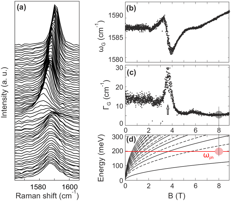
For a more refined comparison of the Raman spectra on both substrates, we seek to suppress the effects on the G line, arising from these differences in charge carrier doping. We therefore minimize the influence of the electronic system on the Raman G line by applying a perpendicular magnetic field. In the presence of a perpendicular magnetic field, the electronic states in graphene condense into Landau levels (LLs). The coupling of these Landau levels to the G mode is well understood ando2007; goerbig2007 and experimentally confirmed yan2010; faugeras2011; qiu2013; faugeras2012; neumann2015; faugeras2009; kossacki2012; kim2013; leszczynski2014. When a LL transition energetically matches the G mode phonon, the position of the G line is shifted and its line width increases. An example for the evolution of the Raman G peak with magnetic field, taken on the hBN sandwich area, is shown in Figure 2a. The individual spectra are offset for clarity. For a detailed analysis, single Lorentzians are fitted to every spectrum. The resulting frequency, , and FWHM, , are displayed in Figures 2b and 2c, respectively. The arrow at T (Figure 2c) indicates a value of the magnetic field where a LL transition is energetically matched with the phonon, leading to a broadening of the G line. However, at a magnetic field of about 8 T, no LL transition is close to the G mode, as illustrated in Figure 2d, where the energies of the relevant LL transitions as a function of magnetic field are compared to the energy of the G mode phonon. Consequently at this high magnetic field the influence of the electronic system on the position and width of the G line is minimized. Note that this effect is independent of the charge carrier density and the exact values of the broadening of the LL transitions assuming that the latter are within a reasonable range as found by other studies kim2013; neumann2015. Thus, the residual broadening of the G line is most likely determined by phonon-phonon scattering and averaging effects over different strain values that vary on a nanometer scale (i.e. sub-spot size length scale see also Supplementary Information).

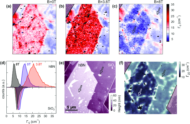
To show that this applies to the entire sample, we first show that the broadening of the electronic states is low enough on the entire hBN-Gr-hBN area. In Figures 3a and 3b, we show maps of at T and 3.8 T, respectively. On the hBN part, the width of the G line shows the resonant behavior depicted in Figure 2c (see also histogram in Figure 3d). This effect happens on all spots on the hBN area, independent of the local doping and strain values and independent of possible local folds and bubbles. The suppression of magneto-phonon resonances on the SiO2 substrate can be attributed to the higher charge carrier density. At higher charge carrier density the needed LL transitions are blocked by the Pauli principle. In a next step, we tune the magnetic field to 8 T, where the electronic influences on the Raman G line are at a minimum. A map of over the entire flake at a magnetic field of 8 T is shown in Figure 3c. Distinct features across the whole sample are visible as regions with increased line width. A comparison with a scanning force microscope image of the sample (Figure 3e) reveals that many of these regions can be associated with folds and bubbles most likely induced during the fabrication process, some of which even cross the border between the underlying hBN and SiO2 substrate regions.
As electronic broadening effects are suppressed at 8 T, the increased line width of the G line in the vicinity of these lattice deformations arises from enhanced phonon-phonon scattering and/or an averaging effect over varying nm-scale strain conditions.
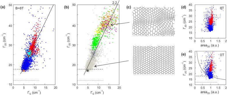
Interestingly, the same features can also be identified in a map recorded at T, shown in Figure 3f. This strongly suggests that the lattice deformations identified at 8 T in also cause a broadening of the 2D mode. The same trend is highlighted in Fig. 4a, where we show the relation of and for all recorded Raman spectra at 8 T. The additional teal data points stem from a graphene-on-SiO2 sample and the orange star originates from a different hBN-Gr-hBN sandwich structure with all data having been obtained at 8 T. Notably, the points from all substrate regions lie on one common line. From this linear relation between and (Figure 4a), we conclude that there must be a common source of line broadening, which is connected to structural deformations. This is mainly due to the fact that at 8 T the G-line broadening is only very weakly affected by electronic contributions (see above). The range of the presented scatter plot can be extended by including data recorded on low-quality graphene samples with significant doping, as shown in Figure 4b. Here, no magnetic field but high doping (corresponding to Fermi energies much higher than half of the phonon energy meV) is used to suppress Landau damping of the G mode, leaving unaffected from electronic contributions. The colored data points are from Raman maps ( T) of CVD (chemical vapor deposition)-grown graphene flakes that were transferred onto SiO2 by a wet chemistry-based transfer. These graphene sheets contain doping values of cm-2, which corresponds to Fermi energies, meV (see suppl. material). The data points show the same trend as the values obtained at 8 T (gray data points in Figure 4b) and even extend the total range of the dependence to higher values of .

While the linear relation between and in Figure 4a and 4b shows that structural deformations also broaden the 2D line, it is less straightforward to identify the actual mechanism of broadening. It is, in principle, possible that the high values of around folds and bubbles are due to a combination of increased phonon-phonon scattering, averaging effects over different strain values within the laser spot and reduced electronic life times. However, interestingly the slopes in Figures 4a and 4b are around 2.2 (see black lines). This is a remarkable resemblance to the strain induced frequency shifts of both modes (compare Figure 1i). This provides very strong indication that averaging over different strain values, which vary on a nanometer scale (see Fig. 4c), play an important role in the broadening of the experimentally observed 2D line. This averaging effect broadens the G and 2D line by the same ratio as their peak positions shift for fixed average strain values explaining the slope of 2.2 between and (see Supplementary Information). We are aware that the low charge carrier densities in the hBN encapsulated area might result in a narrowing of the 2D mode by three to four wave numbers berciaud2013. However, the large differences of on the order of 20-30 cm-1 on both substrates cannot be explained by the differences in charge carrier doping berciaud2013; Stampfer et al. (2007); venezuela2011.
Interestingly, the lowest observed in our experiments are very close to the value that we compute from first-principles as in ref. venezuela2011 (see Supplementary Information for details) assuming an undoped, defect-free and stress-free sample of graphene (horizontal dashed and dotted lines in Figures 4a and 4b). In such an approach, the width of the 2D peak is determined by the anharmonic decay rate of the two phonons involved (5.3 cm-1 according to ref. paulatto2013), and, indirectly, by the broadening of the electron and hole, denoted as in ref. venezuela2011, (see also ref. basko2008). According to ref. venezuela2011, the electron-phonon contribution to is 81.9 meV for electronic states in resonance with the 2.33 eV laser-light. With such a value of we obtain a of 12.1 cm−1 (dotted lines in Figures 4a, 4b and 4e). If, following ref. herziger2014, we double such value of to account for the electron-electron scattering, we obtain a of 17.9 cm-1 (dashed lines in Figures 4a, 4b and 4e), in close agreement with the lowest measured values. In principle, the observed increase of with respect to its minimum value could be attributed to an increase of the electronic broadening , due to doping (increasing the electron-electron scattering) or to the presence of defects (increasing the electron-defect scattering) venezuela2011; basko2008; basko2009. By investigating the relation between and the integrated area of the 2D peak (area2D) we can exclude such a hypothesis. In Figures 4d and 4e we show scatter plots of versus the region-normalized area2D for both B = 8 T and 0 T, highlighting the very weak B-field dependence of . More importantly, we observe that the area of the 2D peak does not depend on , contrary to what is expected in presence of a variation of the electronic broadening venezuela2011; basko2008; basko2009. In particular the measured data does not follow the calculated dependence of on area2D, reported in Fig. 4e, obtained in the calculation by varying electronic broadening . This dismisses differences in the electronic broadening as a main mechanism for the observed variations of .
Finally, our finding that the 2D line depends on nanometer-scale strain inhomogeneities is also in good agreement with high resolution scanning tunneling microscopy measurements, which reveal that graphene on SiO2 forms short-ranged corrugations, while graphene on hBN features significantly more flat areas lu2014.
In summary, we showed that by using a magnetic field of 8 T to strongly suppress the influence of the electronic contributions on the Raman G line width, the latter can be used as a measure for the amount of nm-scale strain variations. Most importantly, we observed a nearly linear dependence between the G and 2D line widths at 8 T independent of the substrate material, indicating that the dominating source of the spread of the broadening of both peaks is the same. From the slope / of around 2.2, we deduce that averaging effects over nanometer-scale strain variations make a major contribution to this trend. Since the 2D line width shows only a very weak dependence on the field, this quantity can even be used without a magnetic field to gain information on the local strain homogeneity and thus on the structural quality of graphene. These insights can be potentially very valuable for monitoring graphene fabrication and growth processes in research and industrial applications, where a fast and non-invasive control of graphene lattice deformations is of great interest.
Acknowledgment
We thank T. Khodkov for support during the measurements. Support by the Helmholtz Nanoelectronic Facility (HNF), the DFG, the ERC (GA-Nr. 280140) and the EU project Graphene Flagship (contract no. NECT-ICT-604391), are gratefully acknowledged. P.V. acknowledges financial support from the Capes-Cofecub agreement.
References
- Novoselov et al. (2012) K. S. Novoselov, V. Fal’ko, L. Colombo, P. Gellert, M. Schwab, and K. Kim, Nature 490, 192 (2012).
- Ferrari et al. (2006) A. Ferrari, J. Meyer, V. Scardaci, C. Casiraghi, M. Lazzeri, F. Mauri, S. Piscanec, D. Jiang, K. Novoselov, S. Roth, and A. Geim, Phys. Rev. Lett. 97, 187401 (2006).
- Graf et al. (2007) D. Graf, F. Molitor, K. Ensslin, C. Stampfer, A. Jungen, C. Hierold, and L. Wirtz, Nano Lett. 7, 238 (2007).
- Ferrari (2007) A. C. Ferrari, Solid State Commun. 143, 47 (2007).
- Yan et al. (2007) J. Yan, Y. Zhang, P. Kim, and A. Pinczuk, Phys. Rev. Lett. 98, 166802 (2007).
- Pisana et al. (2007) S. Pisana, M. Lazzeri, C. Casiraghi, K. S. Novoselov, A. K. Geim, A. C. Ferrari, and F. Mauri, Nat. Mater. 6, 198 (2007).
- Stampfer et al. (2007) C. Stampfer, F. Molitor, D. Graf, K. Ensslin, A. Jungen, C. Hierold, and L. Wirtz, Appl. Phys. Lett. 91, 241907 (2007).
- Mohr et al. (2010) M. Mohr, J. Maultzsch, and C. Thomsen, Phys. Rev. B 82, 201409 (2010).
- Huang et al. (2010) M. Huang, H. Yan, T. F. Heinz, and J. Hone, Nano Lett. 10, 4074 (2010).
- Calizo et al. (2007) I. Calizo, A. Balandin, W. Bao, F. Miao, and C. Lau, Nano Lett. 7, 2645 (2007).
- Balandin et al. (2008) A. A. Balandin, S. Ghosh, W. Bao, I. Calizo, D. Teweldebrhan, F. Miao, and C. N. Lau, Nano Lett. 8, 902 (2008).