Observation of thermally activated glassiness and memory dip in a-NbSi insulating thin films
Abstract
We present electrical conductance measurements on amorphous NbSi insulating thin films. These films display out-of equilibrium electronic features that are markedly different from what has been reported so far in disordered insulators. Like in the most studied systems (indium oxide and granular Al films), a slow relaxation of the conductance is observed after a quench to liquid helium temperature which gives rise to the growth of a memory dip in MOSFET devices. But unlike in these systems, this memory dip and the related conductance relaxations are still visible up to room temperature, with clear signatures of a temperature dependent dynamics.
pacs:
72.20.ee, 72.80.Ng, 73.40.QvSince the pioneering works of Zvi Ovadyahu and coworkers 20 years ago OvadyahuPRB91 , the number of disordered insulating systems in which glassy conductance relaxations have been reported is slowly increasing with time ElectronGlassBook . It gathers now amorphous and micro-crystalline indium oxide films OvadyahuPRB91 , granular aluminium films GrenetEPJB03 , Be films OvadyahuPRB10 , ultrathin and discontinuous films of metals GoldmanPRB98 ; FrydmanEPL12 and thallium oxide films OvadyahuPRB13 . Until very recently, the glassy features like the memory dip and its activationless logarithmic slow relaxation were believed to be of universal character. However a new behaviour was evidenced two years ago in discontinuous metal films FrydmanEPL12 : the conductance relaxations were found to be strongly suppressed below a well-defined temperature T*, whereas nothing similar was seen in indium oxide OvadyahuEPL98 ; OvadyahuPRL07 and granular Al films GrenetEPJB07 , the two most extensively studied systems so far.
These glassy features remain for a large part unexplained but they might be the experimental signature of an electron glass ElectronGlassTheory ; ElectronGlassRecent ; ElectronGlassBook . This hypothesis is supported by the fact that all systems in which out-of-equilibrium effects are observed have a large charge carrier density compared to standard doped semiconductors close to the metal-insulator transition OvadyahuPRL98 ; OvadyahuPRB13 . In indium oxide films, the charge carrier density was indeed found to influence the gate voltage width of the memory dip and the conductance dynamics itself OvadyahuPRL98 , even if aspects of this last result were questioned recently GrenetPRB12 .
In order to make some progress towards the understanding of these phenomena, it is of crucial importance to identify among the observed properties what is universal and what is specific to each system. In this respect, the exploration of new systems is an incomparable source of information. We present here the first investigation of out of equilibrium phenomena in amorphous (a-) insulating NbSi thin films. We show that this system also displays slow conductance relaxations after a quench from room to liquid helium temperature, as well as gate voltage () history memory. However the characteristics of the memory dip as well as the effects of temperature are different from all known systems and strongly indicate a thermal activation of the dynamics OvadyahuPRL07 ; OvadyahuEPL98 ; GrenetEPJB07 .
Our NbSi films were obtained by co-deposition of Nb and Si at room temperature and under ultrahigh vacuum (typically a few mbar) CraustePRB13 . Samples for conductance relaxation measurements (see below) were deposited on sapphire substrates coated with a 25 nm thick SiO underlayer designed to smooth the substrate and were protected from oxidation by a 25 nm thick SiO overlayer. Samples for electrical field effect measurements were deposited on Si++ wafers (the gate) coated with 100 nm of thermally grown (the gate insulator). These were subsequently covered with a 12.5 nm thick SiO overlayer. Previous studies have shown that such films are continuous down to a thickness of 2 nm and that they are amorphous and homogeneous down to the nanometre scale CraustePRB13 . The SiO under- and over- layers were found to play no significant role in the electrical glassy behaviour described below NoteSiO .
Electrical measurements were done either in two or four contacts configurations. Voltage or current bias was limited to low enough values in order to stay in the ohmic regime. The resistance of the films has an exponential-like divergence at low temperature of the form , with .
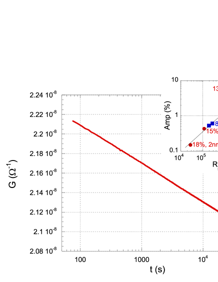
We have first measured the conductance variations of the films deposited on sapphire after a rapid (about 10mn) cooling down from room temperature to liquid helium. Our experimental set-up was already described in details elsewhere DelahayePRL11 . A typical result is shown in Figure 1 for a 2.5nm thick film. Once at 4.2K, the conductance is found to decrease as a logarithm of the time elapsed since the cooling down, with no signs of saturation even after several days of measurements. If we define the relaxation amplitude as the conductance change between 100s and , it reaches 5% in this sample (sheet resistance at 4K of about ). Logarithmic conductance relaxations were found in all the samples we have measured. The relative amplitude of the relaxation increases with but no significant difference was observed between 12.5nm and 2.5nm thick films of similar (see the insert of Figure 1). This is qualitatively similar to what is seen in indium oxide OvadyahuPRB02 ; OvadyahuPRB03 ; OvadyahuPRB06 and granular Al thin films GrenetEPJB07 ; DelahayePRL11 .
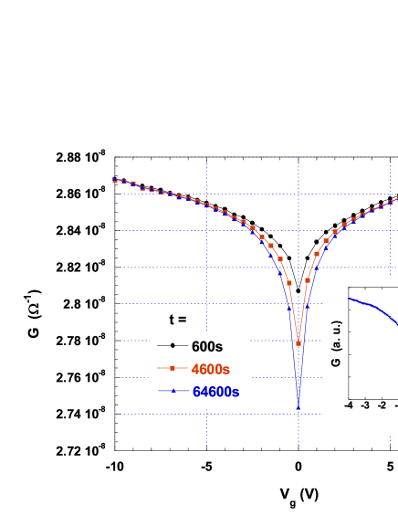
A set of films 2.5nm thick with was also deposited on a Si++/ substrate in order to perform field effect measurements. The films were first cooled down from 300K to 4.2K under a gate voltage of 0V. Once at 4.2K, sweeps from -30V to +30V were repeated at constant time intervals while the value was maintained at 0V between the sweeps. The value maintained between the sweeps is called the “equilibrium” gate voltage and is noted . Typical curves are shown in Figure 2. A conductance dip or memory dip of a few % centred on is clearly visible and its amplitude increases as a function of time. Once again, this is qualitatively similar to what is seen in indium oxide OvadyahuPRB02 and granular Al thin films GrenetEPJB07 ; DelahayePRL11 .
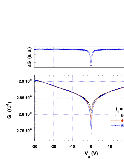
But when the same curves are plotted on a larger scale (see Figure 3), another feature becomes noteworthy. We observe no saturation of the conductance increase when is scanned away from even up to 30V. By contrast, a saturation to a constant value or to a small normal field effect is present in all other systems studied so far. Thus the memory dip, which reflects the sample memory of its history, is unusually wide in NbSi films compared to granular Al films GrenetEPJB07 and highly doped indium oxide films OvadyahuPRL98 , systems exhibiting the broadest memory dips. A value of 30V over a layer of 100nm corresponds to a surface charge density of . In granular Al films the conductance dip at 4.2K is limited to changes of the surface charge densities at least 6 times smaller ( values of about 5V in the scale of Figures 2 and 3). But if the dip is very wide, only part of it is changing after the cooling down. As highlighted by the upper graph of Figure 3, the changes after a cool down at 4.2K are limited to 10V around while the rest of the dip remains unchanged, as if it was frozen.
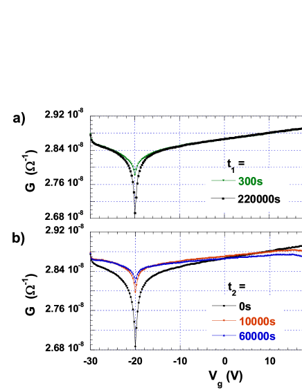
A cooling down from 300K to 4.2K under a different (-20V in Figure 4a) results in a broad dip centred on this new value. Thus both the “frozen” and the growing parts of the dip reflect the memory of the sample. If, at low T, we change from to (Figure 4b), a new dip forms at while the old one centred on is slowly erased. It is noteworthy that the induced relaxation is not limited within 10V around and , but affects the whole range. In other words, the broad “frozen” part is set to relax by a change.
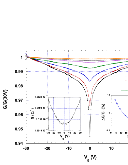
In Figure 5, normalized memory dips are shown at different temperatures from 4.2K up to 36K. They have been measured after a few days at 4.2K under . Since the limits of the dips are out of our available window, it is not possible to define precisely their amplitudes and their widths. However, the relative difference between the conductance measured at and gets smaller under a temperature increase. Interestingly enough, this decrease of the dip amplitude with T appears to be weaker than what was seen in granular Al and indium oxide films OvadyahuEPL98 ; GrenetEPJB07 . A trace of the conductance dip is even visible at room temperature (see the left-side insert of Figure 5) while is of only . The conductance difference between and is then of the order of 0.01%. A room temperature dip was never observed in previously studied systems, except recently in discontinuous Au films made at room temperature FrydmanPrivateCom . The shape of the dip is also temperature dependent: it gets rounder at higher T.
We come now to the T dependence of the conductance relaxation dynamics. Such dependence cannot be revealed simply by measuring the conductance relaxations after a change or a quench at different T. The relaxations are logarithmic in time (see Figure 1) and they thus contain no characteristic times by themselves. More complex protocols have to be used and to this respect, the so called “two dip” protocol turned out to be a powerful tool OvadyahuPRL97 ; OvadyahuPRL98 ; OvadyahuPRB02 . In one version of this protocol, a new conductance dip is formed by fixing to a never explored value during a time (the “writing” step). Then, is changed to a different value and the erasure of the dip amplitude is measured as a function of time (the “erasure” step). It was found in indium oxide and granular Al films that the dip erasure scales with OvadyahuPRL00 ; OvadyahuPRB02 ; GrenetEPJB07 and that the characteristic erasure time is equal to NoteTime , meaning that it takes a typical time to erase a dip formed during a time . This finding can be simply explained by assuming that the writing and the erasure of the memory dip result from the same modes switching back and forth with unchanged characteristic relaxation times under changes GrenetEPJB07 ; AmirPRL09 .
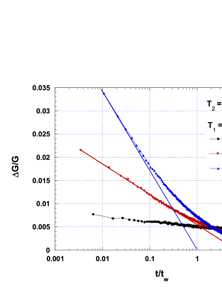
In order to reveal a T dependence of the relaxation dynamics, the writing and the erasure of the dip have to be done at two different T GrenetEPJB07 . In Figure 6, the erasures at of memory dips formed during at different are compared. When , we get a “trivial” result, i.e. it takes a characteristic time of about to erase a dip formed during . But when the writing is done at , the situation is different. Beyond the change of the dip amplitude at short times, the characteristic erasure time, if any, is now larger than (the erasure curve corresponding to is indeed almost constant). Assuming that the same modes are involved in the writing and the erasure of the dip, these results indicate a slow down of the dynamics under cooling: the modes are slower at than at . Similar measurements performed in granular Al films below have revealed no T dependence of the characteristic erasure time: it is always equal to , whatever and GrenetEPJB07 . The results of Figure 6 also suggest that the memory of any visited at various T remains printed at lower T. Further investigations have confirmed that the broad “frozen” part of the dip shown in Figures 3 and 4 reflects the accumulation of memory during the cooling down.
Extensive studies performed in indium oxide and granular Al films have shown that these two systems display very similar glassy features: logarithmic conductance relaxation after a quench and memory dip in MOSFET devices whose dynamics is essentially T independent OvadyahuPRL07 ; GrenetEPJB07 . Since these features were observed in micro-crystalline, amorphous and granular samples, it was tempting to believe that they should be rather universal. A first breach in this universal picture was recently opened by conductance measurements on discontinuous films of metals FrydmanEPL12 . In such films, a memory dip is present but its dynamics is strongly T dependent: the dip is frozen below a temperature T* which is determined by the highest T experienced by the sample, suggesting that a well defined activation energy dominates the dynamics of the system. Since discontinuous films of metals have a very specific (maze) microstructure, it may not be surprising to observe also a specific T dynamics of their memory dip.
Our results demonstrate that non-universal behaviors are not limited to “exotic” microstructures. In a-NbSi films, the dynamics of the memory dip is also found to be T dependent. But in contrary to discontinuous films of metals, the dip responds to changes down to 4.2K, suggesting that its dynamics is governed by a large distribution of activation energies. Why amorphous NbSi films do not behave like amorphous indium oxide films is a challenging question. According to specific heat measurements MarnierosPhysicaB99 , the charge carrier densities of (weakly) insulating a-NbSi films lie in the range of . Such values are similar to the largest charge carrier densities reported in indium oxide films OvadyahuPRL98 . A more promising issue might be to consider the ionic character of the two systems. Indium oxide and NbSi are expected to be respectively ionic and covalent alloys, a difference which should strongly influence the potentiel lanscape and the statistics of the localized states.
In summary, our electrical measurements on a-NbSi films have revealed out-of-equilibrium and glassy features. A slow relaxation of the conductance is seen after a cool down of the films from room temperature to liquid helium and a conductance dip centred on the equilibrium gate voltage is observed in electrical field effect measurements. Compared to granular Al and indium oxide thin films, the dip is very wide, robust under a temperature increase and its dynamics seem to be strongly temperature dependent. Our findings strengthen the fact that important differences exist among the glassy features of disordered insulating systems. They are much more diverse that what was believed until recently and cannot be reduced to the prototypical case of indium oxide films. Theoretical models should also not be restrained to T independent tunneling dynamics. Where these differences come from is a crucial but so far unsolved question. In a-NbSi films, the electrical resistance can be tuned by changing the Nb content, the thickness or by annealing the films up to different temperatures CraustePRB13 . By testing the influence of these parameters on the electrical glassy properties, we have the unique opportunity to better understand their physical origin.
Acknowledgements.
Discussions with O. Crauste and A. Frydman are gratefully acknowledged.References
- (1) M. Ben-Chorin, D. Kowal and Z. Ovadyahu, Phys. Rev. B 44, 3420 (1991).
- (2) M. Pollak, M. Ortuño and A. Frydman, The Electron Glass (Cambridge University Press 2013).
- (3) T. Grenet, Eur. Phys. J. B 32, 275 (2003).
- (4) Z. Ovadyahu, Y.M. Xiong and P.W. Adams, Physical Review B 82 195404 (2010).
- (5) G. Martinez-Arizala, C. Christiansen, D. E. Grupp, N. Marković, A.M. Mack and A.M. Goldman, Phys. Rev. B 57, R670 (1998).
- (6) T. Havdala, A. Eisenbach and A. Frydman, Eur. Phys. Lett. 98, 67006 (2012). A frozen memory dip was indeed already observed 30 years ago in discontinuous gold films in C.J. Adkins, J.D. Benjamin, J.M.D. Thomas, J.W. Gardner, A.J. McGeown, J. Phys. C: Solid State Phys. 17, 4633 (1984).
- (7) Z. Ovadyahu, Phys. Rev. B 88 085106 (2013).
- (8) Z. Ovadyahu, Phys. Rev. Lett. 99, 226603 (2007).
- (9) A. Vaknin, Z. Ovadyahu and M. Pollak, Eur. Phys. Lett. 42, 307 (1998).
- (10) T. Grenet, J. Delahaye, M. Sabra and F. Gay, Eur. Phys. J. B 56, 183 (2007).
- (11) M. Grünewald, B. Pohlman, L. Schweitzer and D. Wurtz, J. Phys. C 15, L1153 (1982); M. Pollak and M. Ortuño, Sol. Energy Mater. 8, 81 (1982); J.H. Davies, P.A. Lee and T.M. Rice, Phys. Rev. Lett. 49, 758 (1982).
- (12) For recent Ref., see C.C. Yu, Phys. Rev. Lett. 82, 4074 (1999); D.N. Tsigankov et al., Phys. Rev. B 68 184205 (2003). M. Müller and L. Ioffe, Phys. Rev. Lett. 93, 256403 (2004); V. Malik and D. Kumar, Phys. Rev. B 69, 153103 (2004); D.R. Grempel, Europhys. Lett. 66, 854 (2004); E. Lebanon and M. Müller, Phys. Rev. B 72, 174202 (2005); A.M. Samoza et al., Phys. Rev. Lett. 101, 056601 (2008); M. Goethe and M. Palassini, Phys. Rev. Lett. 103 045702 (2009); A. Amir, Y. Oreg, Y. Imry, Annual Review of Condensed Matter Physics 2 235 (2011).
- (13) A. Vaknin, Z. Ovadyahu and M. Pollak, Phys. Rev. Lett. 81, 669 (1998).
- (14) T. Grenet and J. Delahaye, Phys. Rev. B 85, 235114 (2012).
- (15) O. Crauste, A. Gentils, F. Couëdo, Y. Dolgorouky, L. Bergé, S. Collin, C. A. Marrache-Kikuchi, and L. Dumoulin Phys. Rev. B 87, 144514 (2013).
- (16) The conductance relaxations of two 12.5nm thick NbSi films deposited on sapphire with and without the SiO underlayer were measured after a quench from room T to 4.2K. We found the same logarithmic decrease with the sample amplitude in both cases. Moreover, field effect measurements on 12.5nm thick films without any SiO overlayer give similar glassy features to what is described below on 2.5nm thick film with a SiO overlayer.
- (17) J. Delahaye, J. Honoré, and T. Grenet, Phys. Rev. Lett. 106, 186602 (2011).
- (18) A. Vaknin, Z. Ovadyahu and M. Pollak, Phys. Rev. B 65 134208 (2002).
- (19) Z. Ovadyahu and M. Pollak, Phys. Rev. B 68 184204 (2003).
- (20) Z. Ovadyahu, Phys. Rev. B 73 214204 (2006).
- (21) The conductance minimum can be moved at 300K to new values after long stays under different .
- (22) A. Frydman, private communication.
- (23) Z. Ovadyahu and M. Pollak, Phys. Rev. Lett. 79 459 (1997).
- (24) A. Vaknin, Z. Ovadyahu and M. Pollak, Phys. Rev. Lett. 84 3402 (2000).
- (25) The characteric erasure time is defined as the intercept between the extrapolated short time logarithmic dependence and the abscissa axis.
- (26) A. Amir, Y. Oreg, and Y. Imry, Phys. Rev. Lett. 103, 126403 (2009).
- (27) S. Marnieros, L. Bergé, A. Juillard and L. Dumoulin, Physica B 259-261, 862 (1999). See also : S. Marnieros, Ph.D. thesis, Paris 11 University, Orsay, France (1998).