The Electron Glass in a three-dimensional system
Abstract
We report on non-equilibrium transport features observed in experiments using three-dimensional amorphous indium-oxide films. It is demonstrated that all the features that characterize intrinsic electron-glasses which heretofore were seen in two-dimensional samples are also observed in field-effect measurements of systems that exhibit three-dimensional variable-range-hopping. In particular, a memory-dip is observed in samples configured with gate. The memory-dip width and magnitude support models that associate the phenomenon with the Coulomb-gap. The memory-dip and the glassy effects disappear once the quenched disorder in the system is reduced and the system becomes diffusive. This happens when the Ioffe-Regel dimensional parameter k exceeds 0.3 which is the critical value for the metal-to-insulator transition in all versions of the amorphous indium-oxides [Phys. Rev. B 86, 165101 (2012)]. This confirms that being in the Anderson localized phase is a pre-requisite for observing the memory-dip and the associated glassy effects. The results of the gating experiments suggest that the out-of equilibrium effect caused by inserted charge extend over spatial scales considerably larger than the screening length.
pacs:
72.80.Ng 73.61.Jc 72.20.EeI Introduction
The out-of-equilibrium transport properties of several Anderson insulators exhibit glassy features such as slow relaxation, slow approach to a steady state, ageing, and other memory effects. These non-equilibrium features were theoretically anticipated and are believed to result from the interplay between disorder and interactions 1 ; 2 ; 3 . This glassy phase, commonly referred to as electron-glass, arises from the competition between quench disorder and Coulomb interactions. It is a generic phenomenon that ought to apply to all degenerate Fermi systems with localized states interacting via a Coulomb potential. Experimental evidence for glassy effects, with slow relaxation of many seconds, has been somewhat scarce and was only reported in two-dimensional (2D) systems 4 , with thickness d180-200Å.
In this work we extend the study to thick amorphous indium-oxide (InO) films that, for sufficiently strong disorder, exhibit 3D hopping conductivity at liquid helium temperatures. The out-of equilibrium properties of these samples exhibit glassy effects characteristic of previously studied electron-glasses These include logarithmic relaxation of the conductance following excitation by a variety of means, and a memory-dip (MD) that has all the earmarks of intrinsic electron-glasses.
The memory-dip disappears at the metal-insulator transition of the material, consistent with the conjecture that the glassy phase is a property peculiar to the Anderson insulating phase.
Of special focus in this work is the question of how the insertion of charge into an interacting electronic system takes it out of equilibrium, and in particular how far the disturbance created in the process propagates into the system. We describe the results of a special protocol involving a combination of excitation agents to deal with these questions. It is shown the perturbation due to charge-insertion propagates deeper into the system than the screening length. The implications of these results to the slow dynamics of the electron-glass are discussed.
II Experimental
II.1 Samples preparation and characterization
Several batches of amorphous indium-oxide (InxO) films were prepared in this study. These were e-gun evaporated onto room-temperature substrates using 99.999% pure In2O3 sputtering target pieces. Two types of substrates were used; 1mm-thick microscope glass-slides, and 0.5m SiO layer thermally grown on 100 silicon wafers. The Si wafers were boron-doped (and exhibited P-type conductivity) with bulk resistivity 210cm, deep into the degenerate regime. These wafers were used as the gate electrode in the field-effect experiments. The microscope glass-slides were mostly used for optical characterization and for Hall-Effect measurements.
Deposition was carried out at the ambience of (1-3)10 Torr oxygen pressure maintained by leaking 99.9% pure O through a needle valve into the vacuum chamber (base pressure 10 Torr). Rates of deposition used for the samples reported here were typically 0.6-0.9 Å/s. Under these conditions, the InO samples had carrier-concentration n in the range (7-8)10cm as measured by Hall-Effect at room temperatures. Film thickness in this study was 75020Å. Rate of deposition and thickness were measured by a quartz thickness monitor calibrated using optical interference measurements on thick MgF films.
As-deposited samples had room-temperature resistivity in excess of 10cm which, for the low temperature studies, had to be reduced by several orders of magnitude. This was achieved by thermal annealing. A comprehensive description of the annealing process and the associated changes in the material microstructure are described elsewhere 5 ; 6 ; 7 . For completeness, we give here a brief summary of the changes occurring during the annealing process.
The main effect of annealing is a 10% increase of material density. The thickness shrinkage upon annealing was directly measured by x-ray interferometry and indirectly as an increase of refractive index 7 . In addition, the visibility of the x-ray interference was highly enhanced following extended annealing, presumably due to the smoothing-out potential-fluctuations 6 . The main change observed in the optical properties of the material is a decrease of the optical-gap 7 . This apparently reflects the enhanced inter-atomic overlap associated with the density increase, leading in turn to wider bands.
The annealing protocol that was used in the current study was as follows: After deposition and initial conductance measurement that, in the initial stages, required the use of electrometer (Keithley 617), the sample was attached to a hot-stage at a constant temperature T, typically 5-10 degrees above room temperature. The resistance R of the sample was observed to slowly decrease over time. Ta was raised by few degrees whenever over 24 hours was less than 1% (and the value of the resistance was still higher than desired). To obtain a sample with that was useful for the measurements reported here took 10-20 thermal cycles. The annealing temperature Ta was limited to 360K to minimize the risk of crystallization. Results of measurement on the series of samples reported in this study were generated from two batches of deposition. The samples used for the low temperature measurements were made from deposited 1mm wide strips. These were cut into 2mm long pieces and indium-contacts were pressed at their ends for electrical connections. Sample length L was typically 1mm.
Hall Effect measurement were carried out on samples that were patterned in a 6-probe configuration using stainless-steel masks. These were prepared during the same deposition as the strips used for the low temperature transport measurements. A standard Hall-bar geometry was used with the active channel being a strip of 1 mm wide, and 10 mm long. The two pairs of voltage probes (that doubled as Hall-probes), were spaced 3 mm from one another along the strip. This arrangement allowed us to assess the large scale uniformity of the samples, both in terms of the longitudinal conductance and the Hall effect. Excellent uniformity was found on these scales; resistivities of samples separated by 1 mm along the strip were identical to within 5%. No change (within the experimental error of 3%) was observed in the hall effect due to annealing (tested for samples with room temperature resistivity smaller than 0.4cm which was the highest in the samples studied in this work).
II.2 Measurements techniques
Conductivity of the samples was measured using a two-terminal ac technique employing a 1211-ITHACO current pre-amplifier and a PAR-124A lock-in amplifier. Except when otherwise noted, measurements reported below were performed with the samples immersed in liquid helium at T=4.1K maintained by a 100 liters storage-dewar, which allowed long term measurements of samples as well as a convenient way to maintain a stable temperature bath. The ac voltage bias was small enough to ensure linear response conditions (judged by Ohm’s law being obeyed within the experimental error).
As in a previous study 6 , we use in this work as a dimensionless measure of disorder: k=(9n) (R=e). This is based on free-electron expressions using the measured room-temperature resistivity and the carrier-concentration n, obtained from the Hall-Effect measurements, as parameters. More details of preparation and characterization of InO samples are given elsewhere 5 ; 6 ; 7 .
Optical excitation was accomplished by exposing the sample to AlGaAs diode (operating at 0.880.05m), placed 15mm from the sample. The diode was energized by a computer-controlled Keithley 220 current-source. The samples were attached to a probe equipped with calibrated Ge and Pt thermometers and were wired by triply-shielded cables to BNC connectors at room temperatures. The effective capacitance of the wires was 20pF but the sample-gate capacitance in the MOSFET-like samples used for the field effect measurements was an order of magnitude larger. This still allowed the use of 40-75Hz ac technique except when the sample resistance exceeded 20M. In the latter case a frequency of 4.8Hz had to be used with some compromise on the signal-noise ratio.
Fuller details of measurement techniques are given elsewhere 8 .
III Results and discussion
III.1 Hopping conductivity and current-voltage characteristics
The behavior of the near-equilibrium (conductance) and steady-state (current-voltage characteristics) properties of the 750Å indium-oxide films used in this work was typical of a variable-range-hopping (VRH) mechanism. Conductance versus temperature G plots of two samples are shown in Fig.1.
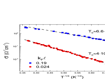
At the 4-35K temperature range G(T) of these samples is consistent with a Mott-type VRH for a three-dimensional (3D) system 9 . Using the theoretical expressions 9 ; 10 for G(T)[-(T/T)], the associated localization length may be obtained from 8 kT3(n) where k is the Boltzmann constant and n is the material’s thermodynamic density of states (DOS) at the chemical potential. For indium-oxide with carrier-concentration n810cm n210ergcm which then gives 14Å and 26Å for the samples depicted in Fig.1. The hopping length r(T) [(T/T)] for these samples is 140Å and 170Å respectively at the lowest temperature studied here (T=4.1K), consistent with 3D variable-range-hopping. It should be remarked that these VRH expressions are based on simplified models 11 and therefore our estimates for and r may be off by a certain factor. Note however, that our estimate of for the more disordered sample in Fig.1 is close to the Bohr radius for indium-oxide (10Å), which is what one expects the localization-length to be for a deeply insulating sample, so our estimates of are probably not so bad.
Another characteristic manifestation of hopping conductivity is the sensitivity of G to an applied electric field. In Fig.2 such a behavior is shown for 3 samples having different degrees of disorder (labeled by their k value).
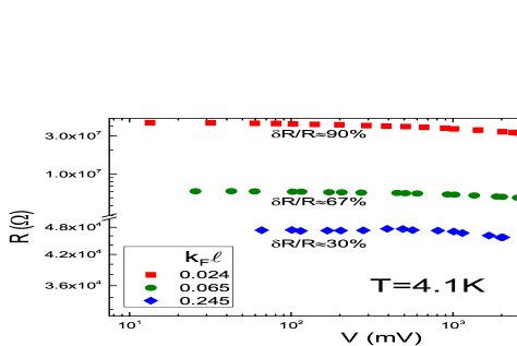
The data in this figure illustrates the dependence of G on voltage. Theories anticipate 12 ; 13 ; 14 ; 15 deviations from linear-response when the applied field F exceeds (kT)/eL where L is of the order of 14 r or the percolation radius 12 L. It is commonly found however that non-ohmicity sets-in at a considerably smaller F than can be attributed to any of these lengths 16 ; 17 . The current case is no exception; deviation from Ohm’s law are observable in these data in fields as small as 10Vm which imply length scales of several microns. Note also that the higher is the disorder (and thus the smaller are both r and L), the smaller is the voltage required to maintain Ohmic behavior. Based on the sample-size dependence for non-Ohmicity in a number of systems, it has been suggested that the anomalous sensitivity of disordered systems to applied fields result from the presence of long range potential fluctuations, which is also revealed in the dependence of non-Ohmic effects on sample-size 18 .
III.2 Out of equilibrium transport properties
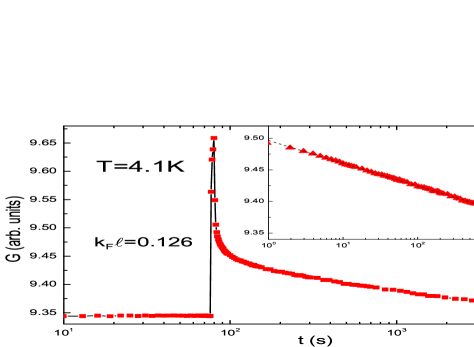
The first indication for non-ergodic behavior is the temporal evolution of G following a sudden cooling process, which is actually the initial stage of every new experiment in this field. All intrinsic electron-glasses exhibit G(t)G- a(t) law after a quench-cooling from room-temperature to a cold enough bath. This usually is carried out in stages; first, the sample, attached to a probe, is cooled to 80-100K and held there for few minutes to lower the heat capacity of the sample-stage and surrounding devices (thermometers, infrared-LED, etc.). Then, the probe is quickly lowered to the liquid helium bath. Measurement of the conductance relaxation versus time may commence once the attached thermometer confirms that a stable temperature has been reached. An example of a typical run is shown in Fig.3.
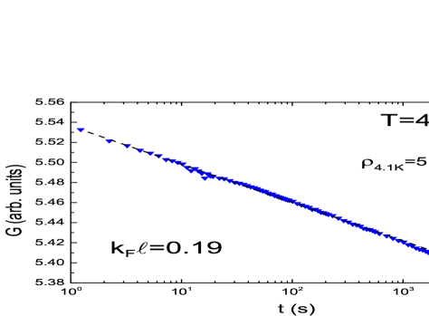
The prefactor a in G(t) is related to the magnitude of the nonequilibrium effects that may be expected for a given sample (relative to its ‘equilibrium’ conductance). As will be discussed below, this information may be useful when evaluating some aspects of the mechanism by which gating the system (or radiating it with infrared source) takes it far from the equilibrium.
Of the many ways to take the system out of the equilibrium the field-effect is arguably the least ”destructive” and the most widely used technique. The field-effect also exposes the identifying signature of the electron-glass - a memory-dip (MD) which appears a minimum in the conductance versus gate voltage G(V) at the gate voltage where the system was allowed to relax. It has been conjectured by several authors 19 ; 20 ; 21 that the MD is a reflection of the Coulomb gap 22 ; 23 ; 24 ; inserting (removing) particles to (from) the system randomizes the electronic system thus destroying the Coulomb-gap (if randomization is complete) and enhancing the conductance. Indeed many of the experimentally observed features seem to be accounted for by this approach 4 . There are questions however as to the underlying excitation mechanism, in particular, it is interesting to know what is the spatial range of the disturbance introduced by a sudden change of the gate voltage. In the next few paragraphs these issues will be discussed using data for the infrared excitation and field effect measurements.
The field effect of one of the studied samples is shown in Fig.4 at different temperatures.
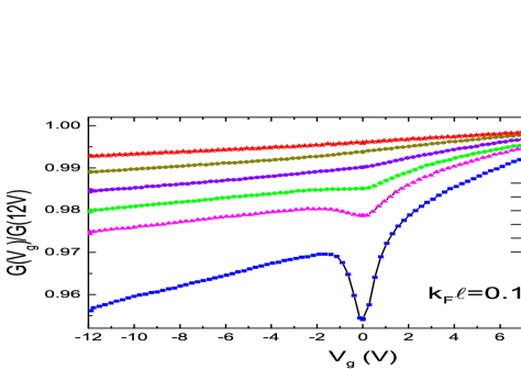
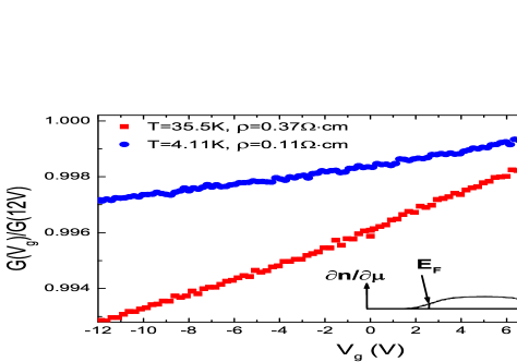
These data, taken on one of the samples depicted in Fig.1, illustrates the evolution of the field effect traces G(V) with temperature. Each curve is composed of an asymmetric (with respect to the equilibrium gate voltage) G(V), reflecting the thermodynamic density of states, and a MD that quickly diminishes in magnitude with temperature. The overall behavior is qualitatively similar to the previously studied temperature dependence of a 2D systems 8 ; 25 . However, the larger range of the V scan here reveals that the modulation produced by the MD extends much further than the ‘half-height’ width consistent with a point made earlier 26 . It also suggests that the thermodynamic part of G(V) is a somewhat concave curve presumably due to a disorder-modified n at the tail of the conduction-band. The Fermi energy E associated with n810cm is near the bottom of the conduction band as illustrated in the schematic drawing in Fig.5. The figure shows G(V) plots for two samples measured under conditions where the MD contribution is negligible and it is interesting to note that the average slope is stronger for the more disordered sample (even though it was measured at a higher temperature).
We have used such a non-linear extrapolated curve as a baseline in estimating the relative magnitude G/G of the MD for a given G(V) as illustrated for example in Fig.6 for one of the samples. The inset to the figure depicts the dependence of the MD magnitude on the sample resistivity (all measured with the same sweep rate at the bath temperature of 4.1K and 24-30 hours after their cool-down).
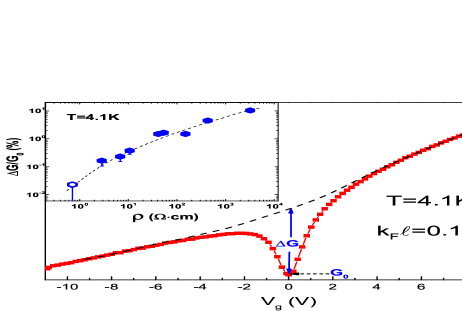
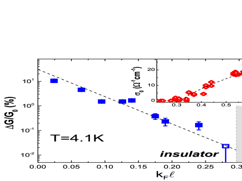
The data in the inset show that the MD magnitude vanishes, faster than a power-law, as decreases. Note that the least resistive sample in this series is assigned with an empty symbol and a downward-going error-mark to indicate that its very small MD has a borderline value in terms of our signal-noise ratio. This sample is actually near the transition to the metallic phase; its k is 0.28 which is within the critical value for this system (k)=0.30.2. Indeed, as illustrated in Fig.7, G/G is an exponential function of k suggesting that the MD (and the associated non-ergodic effects) are peculiar to the insulating phase and vanish at the metal-insulator transition where the system crosses over to the diffusive regime.
This is one of the main results of the work.
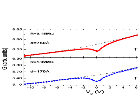
The typical shape and width of the MD in these 3D samples turn out to be remarkably similar to these of a 2D samples of amorphous indium-oxide with comparable carrier-concentration. A comparison between the field effect of two and three-dimensional samples is given in Fig.8.
The nearly identical MD width of the thin versus thick samples is consistent with that the screening-length taken as (n is the relevant scale for assigning an energy scale to the V associated with the MD. In this procedure, used in 4 ; 27 , =(V)C/[e(n)] where C is the sample-to-gate capacitance (per unit area), e is the electron-charge, (n) is the material DOS at the Fermi energy, and V is the range in the G(V) plot modulated by the interaction underlying the MD (presumably, the Coulomb interaction). Note that is the shift of the chemical potential (relative to the band-edge) associated with V.
We digress now to describe another way to drive the system out of the equilibrium; excitation by an electromagnetic field, specifically using infrared radiation. Exciting the system by exposure to infrared radiation will serve as a tool in a more elaborate gating experiments described below.
The IR-protocol has been used 28 on several electron-glasses with different degree of efficiency in terms of randomizing the electronic space-energy configuration (or, simply stated, destroying the Coulomb gap). A plausible route by which IR exposure destroys the Coulomb gap is a two-step process 28 : First, electrons are excited from a localized site to a spatially-overlapping excited state (most likely, an extended state above the mobility edge). Then, a multi-phonon non-radiative process relaxes the system involving sufficiently high energy to overcome the Coulomb gap. Such events should efficiently randomize the electronic configuration. Naturally, there is also a heating effect accompanying the IR radiation, including indirect heating through the sample immediate environment (substrate, sample-stage, the helium bath being heated by the IR LED-case, etc.). It was however demonstrated experimentally that the MD may be completely washed-out by a brief exposure to IR while heating could be ruled out as a significant factor 29 . The heating effect may be separated from the optical excitation part: Moderate heating (raising the bath temperature by T/T1), induces a slow process requiring a long time for the randomization to become appreciable 30 . This is so because only the high energy phonons in the Bose-Einstein distribution tail are relevant for the process. The degree of randomization may be tested by performing a quick G(V) sweep; absence of the MD indicates complete randomization.
The results of two IR protocols, one where the IR exposure is brief, and the other where it is allowed to operate on the system for an extended time are shown in Fig.9 and Fig.10.
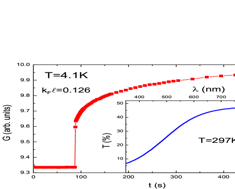
The inset In Fig.9 confirms that the relaxation of the excess conductance created by the IR burst has a logarithmic time dependence with essentially the same slope as that of the quench-cooling process, and in particular, it differs from the ”persistent-photoconductivity” phenomena well known in semiconductors 31 in that it apparently decays to its near-equilibrium value without the need to wait an astronomical time or raise the bath temperature to regain the pristine, near-equilibrium conductance. However, only in rare cases is it possible to completely wash-out the MD with just a brief IR burst. To achieve a complete randomization, required for the experiment described in the next paragraph, we employ the ‘extended IR-protocol’ shown in Fig.10. Here the IR radiation is kept for few minutes while G is monitored and is observed to monotonously increase. The situation is qualitatively similar to that encountered with either, the ‘stress-protocol’ or when the bath temperature is raised by a small T, in both cases the excitation involves generation of phonons 30 . The IR-protocol is very efficient; it destroys the MD in a matter of minutes under a moderate change of G in the excitation stage, which is not possible with any of the ”thermal” methods. Using the IR for erasing the MD allows us to learn about the spatial range of the disturbance created by changing the gate voltage with a much better time resolution than possible with the quench-cooling protocol (where one has to wait longer for the ambient temperature to reach its stationary value). The protocol involved in these experiments is explained next, and the results of this protocol for a particular sample are shown in Fig.11.
Starting from a near-equilibrium state with the sample under V=0, the IR source is turned on for 10 minutes. Then, V is quickly swept to V=10.8V while G(V) is recorded. The gate voltage is now quickly swept back and parked at V=0 for a certain time, allowing the sample to resume the build-up of a memory-dip at this gate voltage. Next, another V sweep is taken and a new G(V) is obtained, now exposing a ”half-MD”. (In these experiments we measure just the positive V range of the G(V) trace for the sake of minimizing the time the system is disturbed by the ”exploratory” sweeps). The process is then repeated at different time intervals.
Note first that the conductance at V=0 decreases logarithmically for both G(t,V=0) taken by the field-effect sweeps and G(t) for the quench-cooling protocol. Moreover, both relaxations proceed at essentially the same rate (in terms of G/decade). This demonstrates that the extended IR-protocol could be as efficient as the cooling-protocol in randomizing the entire volume of the system. The IR protocol is however much more convenient, quick and less susceptible to cause sample-damage than the thermal recycling involved in the cooling-protocol.
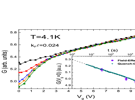
Turning now to the details of the main plot it is of interest to find out what is the range in G(V) over which the modulation due to the MD is appreciable. Adopting the scheme proposed in 26 , we take this range to be defined by the gate-voltage V* where the G(t,V) plots merge with the ‘thermodynamic’ curve. The signal-to-noise ratio in the data of Fig.10 (measured at low frequency because of the relatively large R of this particular sample), makes it difficult to put a value for V*. The IR+gate protocol was therefore repeated on samples with smaller resistivities and the results of the combined IR+gate protocol for two of them are shown in Fig.12.
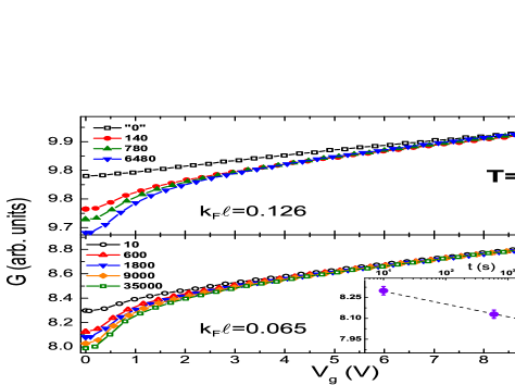
There are two feature revealed by these data. The first is that the modulation associated with the MD extends to V of the order of 6-7 volts, which is about an order of magnitude higher than estimated from the ‘half-height’ width that was the basis of the energy-scale estimate of Vaknin et al 25 . This extended range may also be recognized from the data in Fig.4 above. As pointed out in 26 this result makes the range in energy associated with the MD in line with the expectation of models based on the Coulomb-gap being the mechanism underlying the memory-dip 19 ; 20 ; 21 .
The second feature is more intriguing: The G(t,V) traces in Fig.11 and Fig.12 converge to common value for VV*, independent of the time that elapsed since the system began relaxing after being randomized by either the quench-cooling or the IR-protocol. During this time, the system was relaxing at V=0 except for the brief sojourns made by sweeping V towards 11-12V, that interrupted the relaxation by inserting new charges into the sample. The time independence of the G(t,VV*) traces therefore suggests that the gate sweep affects the entire volume of the sample.
This is not a trivial result: It might have been expected that, since the time of sweep is shorter than the ”Maxwell-time”, the excess charge induced by V resides in the layer of extent , the Thomas-Fermi length (which is 10Å in this system), at the sample-spacer interface, and the parts of the sample that are outside of the Coulomb interaction range cannot be aware of the disturbance caused by V. The sample conductance would then continue to relax uninterrupted by the gate. This will then result in G(t) traces that for VV* obey a logarithmic relaxation like G(t,V=0) albeit with a smaller slope (a behavior seen in granular films thicker than 10nm 32 ). Our results, where the excitation by charge insertion is as complete as quench-cooling for such thick films, is hard to reconcile with such a simple Coulomb-induced mechanism by which the system gets out of equilibrium. If the range of excitation was limited to the spatial range of the Coulomb interaction, the gate excitation might have been progressively less effective for film thickness exceeding the hopping length, which is the natural screening length in VRH.
It is natural to expect that above a certain film thickness the gate-protocol will be less effective, and studying thicker films would be of interest. It is not clear however that it is the stationary screening-length that is the relevant length-scale. This scenario ignores the many-body aspects of the process of charge insertion into an interacting system. Pollak was the first to recognize the complexity of the situation in his Coulomb-gap paper 23 . The many-body processes that accompany inserting charge into the interacting system are complicated; some transitions are induced by direct Coulomb interactions but polarization fields, may induce further transitions via dipole forces to lower the system energy 23 . In other words, the disturbance due to the added charge propagates through the system via both, Coulomb interaction causing direct transitions, and by ‘after-shock’ events of various nature moving the disturbance further into the system. A similar scenario, depicting the spread of the disturbance due to the inserted-charge as ‘avalanches’, was recently simulated by Palassini and Goethe 33 .
The problem is further compounded by the inhomogeneous nature of the medium, which is an inherent property of the hopping regime. The widely disparate values of local conductivities of which the medium is composed introduces a wide spectrum of times involved in the process of charge spreading. The time it takes the medium to approach equal potentiality, while apparently 34 still shorter than the V sweep-time, is distributed over a wide spectrum and cannot be simply related to the Maxwell-time associated with the measured sample conductivity.
In sum, we presented data on the transport properties of thick InO films. In their insulating phase ( k0.3) these films exhibit variable-range-hopping conductivity and current-voltage characteristics that are commonly found in other insulating systems at low temperatures. Field effect measurements reveal a well developed memory-dip which is the identifying feature of all intrinsic electron-glasses 26 . Following excitation, by either, quench-cooling, exposure to IR radiation, or a sudden change of carrier-concentration, they exhibit logarithmic relaxation characteristic of other electron-glasses. Their non-equilibrium transport features disappear at the metal-insulator transition. This complements the observation made on 2D systems where the glass phase is likewise restricted to the strongly localized regime.
Experiments with the combined IR exposure and gate excitation protocol reveal that inserting charge into the electron-glass is effective in ‘rejuvenating’ the system over a spatial-range considerably larger than the hopping-length. This seems to suggest that this is a multi-stage process involving many-body effects similar to that treated by Levitov and Shytov for a diffusive system 35 . The localization of the electronic states and the inhomogeneous nature of the medium make such a treatment a challenging task.
In discussing the reasons for the sluggish relaxation of electron-glasses 4 it was suggested that building up the Coulomb-gap from the out of equilibrium, random distribution, involves many more sites than those participating in dc transport. The long range over which the inserted charge affects occupation of localized sites found it this work suggests that the contribution of ‘dead-wood’ regions to the relaxation may be substantial. Local dynamics in these regions is orders of magnitude slower than that of the sites that are part of the current-carrying-network. As long as the latter can communicate, directly or indirectly, with sites in the dead-wood regions, the time it takes the Coulomb gap to establish itself will be influenced by these regions and therefore their effect on the relaxation dynamics of the system has to be considered.
Acknowledgement 1
This research has been supported by a grant administered by the Israel Academy for Sciences and Humanities.
References
- (1) M. Grünewald, B. Pohlman, L. Schweitzer, and D. Würtz, J. Phys. C, 15, L1153 (1982).
- (2) J. H. Davies, P. A. Lee, and T. M. Rice, Phys. Rev. Lett., 49, 758 (1982); ibid, Phys. Rev. B 29, 4260 (1984).
- (3) M. Pollak and M. Ortuño, Sol. Energy Mater., 8, 81 (1982); M. Pollak, Phil. Mag. B 50, 265 (1984); Ariel Amir, Yuval Oreg, and Yoseph Imry, Phys. Rev. B 77, 165207 (2008); ibid. Annu. Rev. Condens Matter Phys. 2, 235 (2011); For a recent review and relevant literature see: M. Pollak, M. Ortuño and A. Frydman, ”The Electron Glass”, Cambridge University Press, 2013.
- (4) Z. Ovadyahu, Phys. Rev. B 88, 085106 (2013).
- (5) Z. Ovadyahu, B. Ovryn and H.W. Kraner, J. Elect. Chem. Soc. 130, 917 (1983); Z. Ovadyahu, J. Phys. C: Solid State Phys., 19, 5187 (1986).
- (6) U. Givan and Z. Ovadyahu, Phys. Rev. B 86, 165101 (2012).
- (7) Z. Ovadyahu, Phys. Rev B 47, 6161 (1993).
- (8) A. Vaknin, Z. Ovadyahu, and M. Pollak, Phys. Rev. B 65,134208 (2002).
- (9) N. F. Mott and A. E. Davis, Electronic Processes in Non-Crystalline Materials, (Oxford University) (1971).
- (10) C. H. Seager and G. E. Pike, Phys. Rev. B 10, 1435 (1974).
- (11) M. H. Brodsky and R. J. Gambino, Journal of Non-Crystalline Solids, 8-10, 739 (1972).
- (12) R. M. Hill, Philos. Mag. 24, 1307 (1971)
- (13) B. I. Shklovskii, Fiz. Tekh. Poluprovodn. 6, 2335 (1972) [Sov.Phys. Semicond. 6, 1964 (1973)]; B. I. Shklovskii, Fiz. Tekh. Poluprovodn. 6, 2335 (1972) [Sov.Phys. Semicond. 6, 1964 (1973)]; B. I. Shklovskii, Fiz. Tekh. Poluprovodn. 10, 1440 (1976) [Sov.Phys. Semicond. 10, 855 (1976)].
- (14) M. Pollak and I. Riess, J. Phys. C9, 2339 (1976).
- (15) N. Apsley and H. P. Hughes, Philos. Mag. 31, 1327 (1975).
- (16) T. F. Rosenbaum, K. Andres, and G. A. Thomas, Solid State Commun., 35, 663 (1980)..
- (17) S. M. Grannan , A. E. Lang, E. E. Haller, and J .W. Beeman, Phys. Rev. B 45 4516 (1992 ); Ning Wang, F. C. Wellstood, B. Sadoulet, E. E. Haller, and J. Beeman, Phys. Rev. B 41, 3761 (1990).
- (18) D. Kowal and Z. Ovadyhau, Physica C, 468, 322 (2008).
- (19) C. C. Yu, Phys. Rev. Lett., 82, 4074 (1999); C. C. Yu Phil. Mag. B, 81, 1209 (2000).
- (20) Eran Lebanon, and Markus Mueller, Phys. Rev. B 72, 174202 (2005); M. Müller and E. Lebanon, J. Phys. IV France, 131, 167 (2005).
- (21) Y. Meroz, Y. Oreg and Y. Imry, EPL, 105, 37010 (2014).
- (22) M. Pollak, Discuss. Faraday Soc. 50, 13 (1970).
- (23) G. Srinivasan, Phys. Rev. B 4, 2581 (1971).
- (24) A L Efros and B I Shklovskii , J. Phys. C 8, L49 (1975); A. L. Efros, J. Phys. C: Solid State Phys 9, 2021 (1976).
- (25) A. Vaknin Z. Ovadyahu, and M. Pollak, Europhys. Letters 42, 307 (1998).
- (26) Z. Ovadyahu, Phys. Rev. B 78, 195120 (2008).
- (27) A. Vaknin, Z. Ovadyahu, and M. Pollak, Phys. Rev. Lett., 81, 669 (1998).
- (28) Z. Ovadyahu, Phys. Rev. B 83, 235126 (2011).
- (29) V. Orlyanchik, A.Vaknin, Z. Ovadyahu, and M. Pollak, Phys. Stat. Sol., b230, 61 (2002).
- (30) Z. Ovadyahu, Phys. Rev. B 73, 214208 (2006).
- (31) See for example: Elena Vateva and Diana Nesifzva, Journal of Non-Crystalline Solids, 90 497 (I987).
- (32) J. Delahaye, J. Honor´e, T. Grenet, Phys. Rev. Lett.,106, 186602 (2011).
- (33) Matteo Palassini and Martin Goethe, Journal of Physics: Conference Series 376, 012009 (2012). A previous simulation work on screening was done by: S. D. Baranovskii, B. I. Shklovskii, and A. L. Efros, Zh. Eksp. Teor. Fiz. 87, 1793 (1984) [JETP, 60, 1031 (1984)].
- (34) Measurements of the charging current during the gating process (Fig.4 in 8 ) show that, at least most of the charge, gets in faster that the temporal-resolution of the field-effect experiments.
- (35) L.S. Levitov, and A. V. Shytov, Pisma Zh. Eksp. Teor. Fiz. 66, 200 (1997) [JETP Lett. 66, 214 (1997)].