Magnetoresistance of disordered graphene: from low to high temperatures
Abstract
We present the magnetoresistance (MR) of highly doped monolayer graphene layers grown by chemical vapor deposition on 6H-SiC. The magnetotransport studies are performed on a large temperature range, from = 1.7 K up to room temperature. The MR exhibits a maximum in the temperature range K. The maximum is observed at intermediate magnetic fields ( T), in between the weak localization and the Shubnikov-de Haas regimes. It results from the competition of two mechanisms. First, the low field magnetoresistance increases continuously with and has a purely classical origin. This positive MR is induced by thermal averaging and finds its physical origin in the energy dependence of the mobility around the Fermi energy. Second, the high field negative MR originates from the electron-electron interaction (EEI). The transition from the diffusive to the ballistic regime is observed. The amplitude of the EEI correction points towards the coexistence of both long and short range disorder in these samples.
I Introduction
Graphene is a newly discovered electronic material which attracts a lot of attention, for both potential applications and unique physical properties Geim (2011). For electronics, the improvement of the graphene quality requires the identification of the main sources of scattering which limit the mobility and this is usually done by transport experiments Tikhonenko et al. (2008); Ponomarenko et al. (2009); Monteverde et al. (2010); Guignard et al. (2012). At intermediate magnetic fields, between the realms of weak localization and quantum Hall effect, recent measurements highlighted the role of the electron-electron interaction (EEI) on the magnetoconductivity.Kozikov et al. (2010); Jouault et al. (2011); Jobst et al. (2012); Iagallo et al. (2013) A complete theory of EEI in graphene is still missing, but it is possible to use the knowledge accumulated in more conventional two-dimensional systems like thin metal films or semiconductor heterostructures, for which EEI has been theoretically and experimentally studied over more than three decades Altshuler and Aronov (1985); Bergmann (1984); Mirlin et al. (2001); Polyakov et al. (2001); Minkov et al. (2003); Goh et al. (2008). The quantum correction due to the EEI differs at low and high temperatures. When the effective interaction time, , is larger than the transport time , the electrons experience many collisions during their interaction: they are in a diffusive regime and the correction of the zero-field conductivity follows a logarithmic dependence on the temperature. When , electrons collide at most with one impurity. This ballistic regime leads to linear-in- corrections to the zero-field conductivity.
A first complete theory, unifying both regimes, was developed Zala et al. (2001) but is only valid if impurities can be considered as point-like scatterers. This condition is satisfied in Si metal-oxide-semiconductor field effect transistor (MOSFET) Pudalov et al. (2003); Shashkin et al. (2002) and in some semiconductor heterostructures, where carrier scattering is dominated by background impurities Coleridge et al. (2002); Proskuryakov et al. (2002). In graphene, the validity of this theory is questionable as the dominant scattering depends on both the graphene quality and the characteristics of the environment. Peres (2010) In this paper, we will rely on a more recent theory Gornyi and Mirlin (2004) which predicts the EEI correction at all temperatures for both short and long ranges disorder. Besides, EEI in graphene is specifically sensitive to the type of disorder, both in the diffusive Kozikov et al. (2010); Jobst et al. (2012) and ballistic regimes with unusual temperature dependencies. In particular, in the ballistic regime, EEI depends on the impurity type Cheianov and Fal’ko (2006) and can give indications on the microscopic nature of disorder in graphene. Up to now, most of the EEI measurements in graphene have focused on the diffusive regime Kozikov et al. (2010); Jouault et al. (2011); Jobst et al. (2012); Iagallo et al. (2013). The systematic study of EEI correction in this material, from the diffusive to the ballistic regime, associated with quantitative and qualitative comparisons with models of disorder, is still lacking. This is the scope of this paper.
II Methods
The samples are large and homogeneous single graphene layers obtained by chemical vapor deposition using propane-hydrogen mixtures.Michon et al. (2010, 2013) Depending on the growth conditions, either the samples are hole-doped and the graphene lies on a hydrogen-passivated SiC surface, or they are -doped and the graphene lies on a carbon-rich buffer layer. Riedl et al. (2009); Jabakhanji et al. (2014). Because of their large size, their good spatial homogeneity, these samples are especially well suited for the analysis of weak localization and EEI.
After the growth, Raman Spectra are recorded using an Acton spectrometer fitted with a Pylon CCD detector and a 600 grooves/mm grating. The samples are excited with a 532 nm (2.33 eV) continuous wave frequency doubled Nd:Yag laser through a 100 objective (numerical aperture 0.9). The full width at half maximum of the focused laser spot is about 400 nm.
Electrical measurements are performed on or 20 m-wide Hall bars processed by electron beam lithography. The Hall bar geometry has been chosen to minimize the current deflection, and follows the technical guidelines which are in use for metrological measurement of the quantum Hall effect. The distance between adjacent lateral probes corresponds to the sample width. The ohmic contacts are fabricated by metal deposition of Pd/Au with an ultra-thin Ti sublayer. The samples are covered by PMMA for additional protection. The magnetoresistivities are measured by lock-in amplifiers with low-frequency currents ( Hz, A) in a variable temperature insert from K up to room temperature. Magnetic fields in the range 0-8 T are used.
In total, we investigated five samples, whose parameters are given in Table 1. Samples S1, S2 and S5 have been done with similar growth procedures. The SiC substrate is their case is hydrogen passivated, and the graphene is -doped. Samples S3 and S4 have been done with another growth procedure, at a higher temperature. The graphene is -doped and resides on a carbon-rich interface. For details, see Ref. Jabakhanji et al. (2014). This paper presents mainly the results obtained for samples S1 and S2. The data obtained for samples S3-S5 lead to similar conclusions and are discussed in the last section.
| Sample | |||||
|---|---|---|---|---|---|
| S1 | 6.9 | 2770 | 3500 | 79 | 17 |
| S2 | 7.4 | 2560 | 3700 | 71 | 14 |
| S3 | -2.0 | 3000 | 1800 | 50 | 18 |
| S4 | -3.1 | 2300 | 2400 | 50 | 14 |
| S5 | 6.2 | 2400 | 3400 | 70 | 18 |
III Results
The inset of Fig. 1(a) shows the zero-field resistivity of sample S1. From 300 K down to 30 K, it decreases with . This is related to the slight mobility increase from up to cm2V-1s-1 between K and K, while the hole density remains constant for this temperature range and is equal to cm-2. Below K, the resistivity saturates at , which gives a constant carrier mobility = cm2V-1s-1 and a transport scattering time fs.
Figure 1(a) shows the longitudinal magnetoresistivity for sample S1, measured at several temperatures up to = 80 K. Above T, Shubnikov-de Haas (SdH) oscillations emerge. The analysis of the damping of the oscillations, as detailed in the Appendix, gives a quantum scattering time of = 17 fs. The large ratio 4.5 at K reveals the presence of long-range disorder. Either long range scattering governs both and , or there is a mixed disorder situation where long and short range scatterings dominate and respectively. In both cases, the presence of long range disorder indicates that Ref. Gornyi and Mirlin (2004) is appropriate for the analysis of the EEI interaction.
Below 30 K, shows the typical features of EEI in the diffusive regime: it is almost perfectly parabolic and its curvature decreases logarithmically with . Moreover, all curves taken at different cross at , as expected by the theory. Altshuler and Aronov (1985) Between 30 K and 80 K, remains parabolic but increases with as phonon scattering is not negligible. Above 80 K, is not parabolic anymore and a flat region starts to develop at low fields . Gornyi and Mirlin (2004); Li et al. (2003)
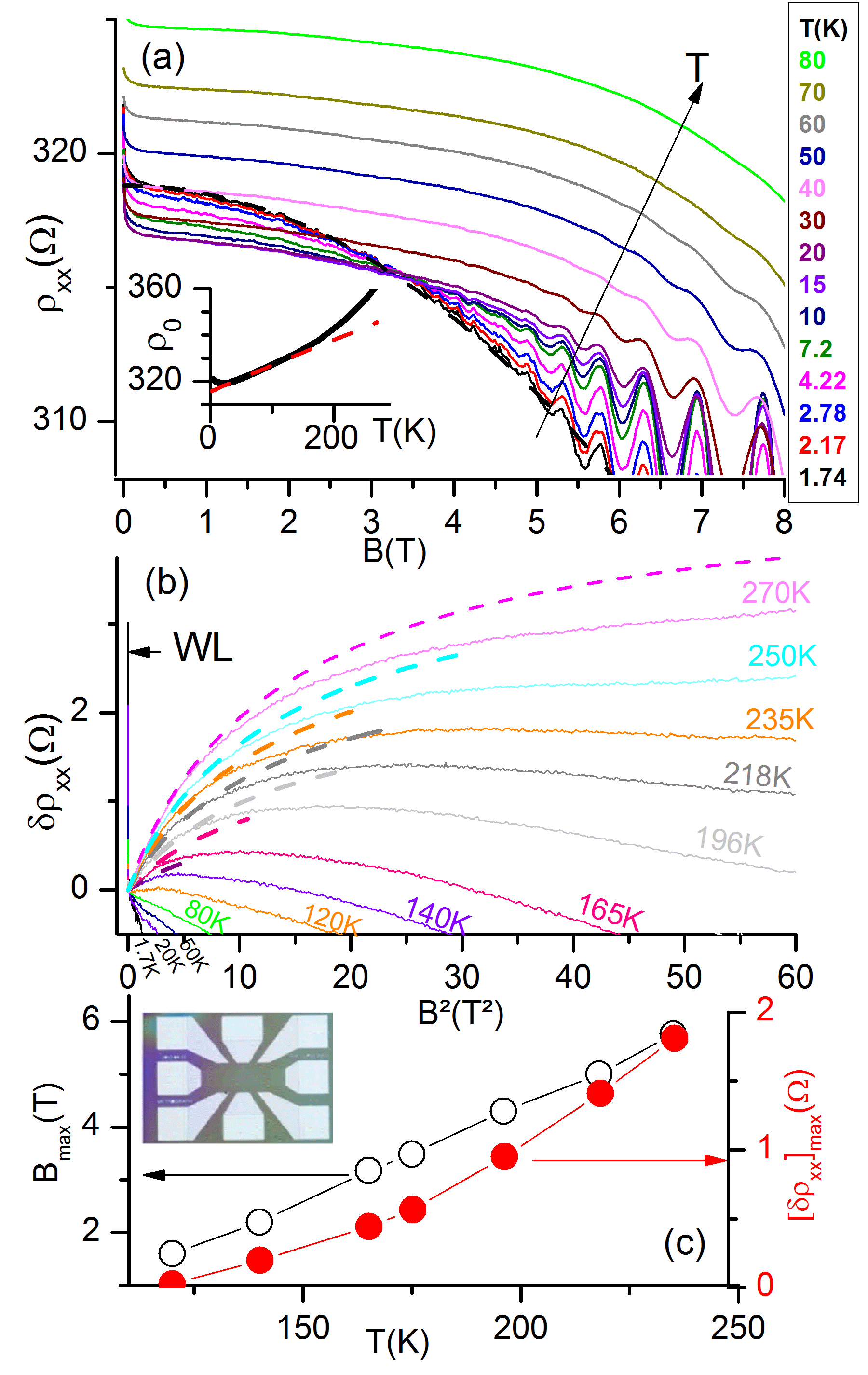
The MR data at higher have been drawn in Fig. 1(b) as vs , where . The magnetic field reference = 300 mT has been chosen to minimize the effects of weak localization which is visible at lower . Above 80 K, an unexpected feature appears: the magnetoresistance is positive at low magnetic field, reaches a maximum and then decreases at higher field. The magnetic field position and the amplitude of this resistance maximum are plotted in Fig. 1(c). The peak position shifts linearly from T to T as a function of the temperature with a slope of T/K. This value is very close to the condition which gives a slope equal to T/K. As is one of the conditions required (with ) to observe the EEI correction in the ballistic regime in Ref. Gornyi and Mirlin (2004), it is legitimate to attribute the negative MR (NMR) on the high- side to EEI, but the positive MR (PMR) at low fields also needs an explanation.
Finally, on almost the whole temperature range, a weak localization (WL) peak is also visible at 300 mT. The attribution of this peak to WL is straightforward, as it gives a correction to the resistivity with the expected amplitude and temperature dependence: . Kechedzhi et al. (2007) At the contrary, there is no sign of weak antilocalization (WAL). While WAL can also give rise to a positive magnetoresistance, both WAL and WL should disappear when increases. This was experimentally verified by Tikhonenko et al. Tikhonenko et al. (2008) who observed that at K WAL disappears due to rapid dephasing of the electron trajectories. In our work, the amplitude of the positive magnetoresistance increases continuously with the temperature and consequently cannot be attributed to WAL.
IV Discussion
IV.1 Magnetoresistance maxima
We first compare our results with previous investigations of MR maxima in other semiconductor structures. Kuntsevich et al. reported the existence of a similar maximum of the magnetoresistivity in the ballistic regime in various Si and GaAs two dimensional electron gases.Kuntsevich et al. (2009) They showed that the maximum presents a universal behavior vs temperature, which we also retrieve for our samples: (i) it is a small effect, less than ( in our case, which corresponds to a conductivity correction of the order of ), (ii) it appears for not too-low temperatures (, in this work) and, (iii) the MR maximum grows and moves to higher field as increases, in accordance with Figs. 1(c). Furthermore, the authors pointed out discrepancies between their experimental results and the available theory of Sedrakyan and Raikh, which predicts a non-monotonic behavior of the magnetoresistance.Sedrakyan and Raikh (2008) This theory predicts a -independent maximum in the magnetoresistivity at , and a decrease of the amplitude of the maxima when increases. These predictions do not correspond to our experimental situation, see Fig. 1(c). Quasiclassical memory effects are also known to lead to strong PMR in the presence of smooth long-range disorder or mixed disorder.Mirlin et al. (1999); Polyakov et al. (2001) However, this effect is temperature independent. Finally, a MR maximum was recently detected in epitaxial graphene, see Fig. 4 of Ref. Iagallo et al. (2013) but its interpretation in terms of EEI corrections led to anomalous values of the interaction parameter.
IV.2 PMR and thermal averaging
We attribute the resistance maximum to a competition between a PMR at low field induced by energy averaging within the temperature window around , and the NMR due to EEI which persists at high fields. In the framework of the relaxation time approximation, the conductivities and are given by:Das Sarma et al. (2011); Alekseev et al. (2013)
| (1) |
where the brackets correspond to
| (2) |
is the energy with respect to the Dirac point, is the Fermi distribution function. The magnetoresistance is then calculated as This expression will give rise to PMR if cannot be taken out of the brackets in the above equations, i.e. if depends on . Then, for our experimental situation and at low magnetic fields, , where the factor arises due to the weak -dependence of the mobility near the Fermi energy. Alekseev et al. (2013)
To show this on a more formal level, we model the PMR by introducing scattering by phonons and ionized impurities. Graphene phonon scattering is given by Hwang and Das Sarma (2008):
| (3) |
where eV is the expected deformation-potential coupling constant, Hwang and Das Sarma (2008); Kozikov et al. (2010) gcm-2 is the graphene mass density and m/s the phonon velocity. Hwang and Das Sarma (2008) Ionized impurity scattering can be calculated within the Thomas-Fermi approximation: Das Sarma et al. (2011)
| (4) |
Here, is the interaction parameter, is the averaged dielectric constant of the environment, the concentration of ionized impurities. The mobility , where is the cyclotron mass, is calculated by using the Matthiessen rule: Within this model, the experimental temperature dependence of the resistivity is well reproduced between 1.7 K and 150 K, as indicated by the fit reported in the inset of Fig. 1(a). The deviation from the fit remains small at higher temperatures and does not exceed 6%. The overall weak and linear increase of the resistivity with confirms that the graphene is well decoupled from the phonon modes of the interface, as expected when the SiC interface has been hydrogenated. Jabakhanji et al. (2014) Fig. 1(b) shows that the correction can also fit satisfactorily the amplitude of the PMR, as well as its slope at low . A direct estimate of from the theoretical dielectric constants of SiC ( =9.66) and PMMA () leads to . This gives good fits with as the fitting parameter. Nevertheless, this overestimates the PMR by 25% at room temperature. To get an even better agreement we used both and as fitting parameters. The best fits shown in Fig. 1(a) and (b) have been obtained for and . The largest part of the PMR comes from the screening term in . If this term is neglected, there is no PMR induced by ionized impurities and the model fails as the PMR induced by phonon scattering alone is too small. Other mechanisms have been considered: polar optical phonons from the PMMA Fratini and Guinea (2008) give a very small PMR. Very little is known on the phonons of the SiC/graphene hydrogenated interface. Phonons of the non-hydrogenated SiC/graphene interface give, by a deformation potential, a dependence () Ray et al. (2012), which suggests that in the case of hydrogenated interface, this mechanism does not contribute to the magnetoresistance. Short range and resonant scatterers have not been included for simplicity in the model. They give a relative PMR five times larger than the one observed. Combining all this, ionized impurities are one of the most probable sources of the observed PMR.
IV.3 NMR and EEI correction
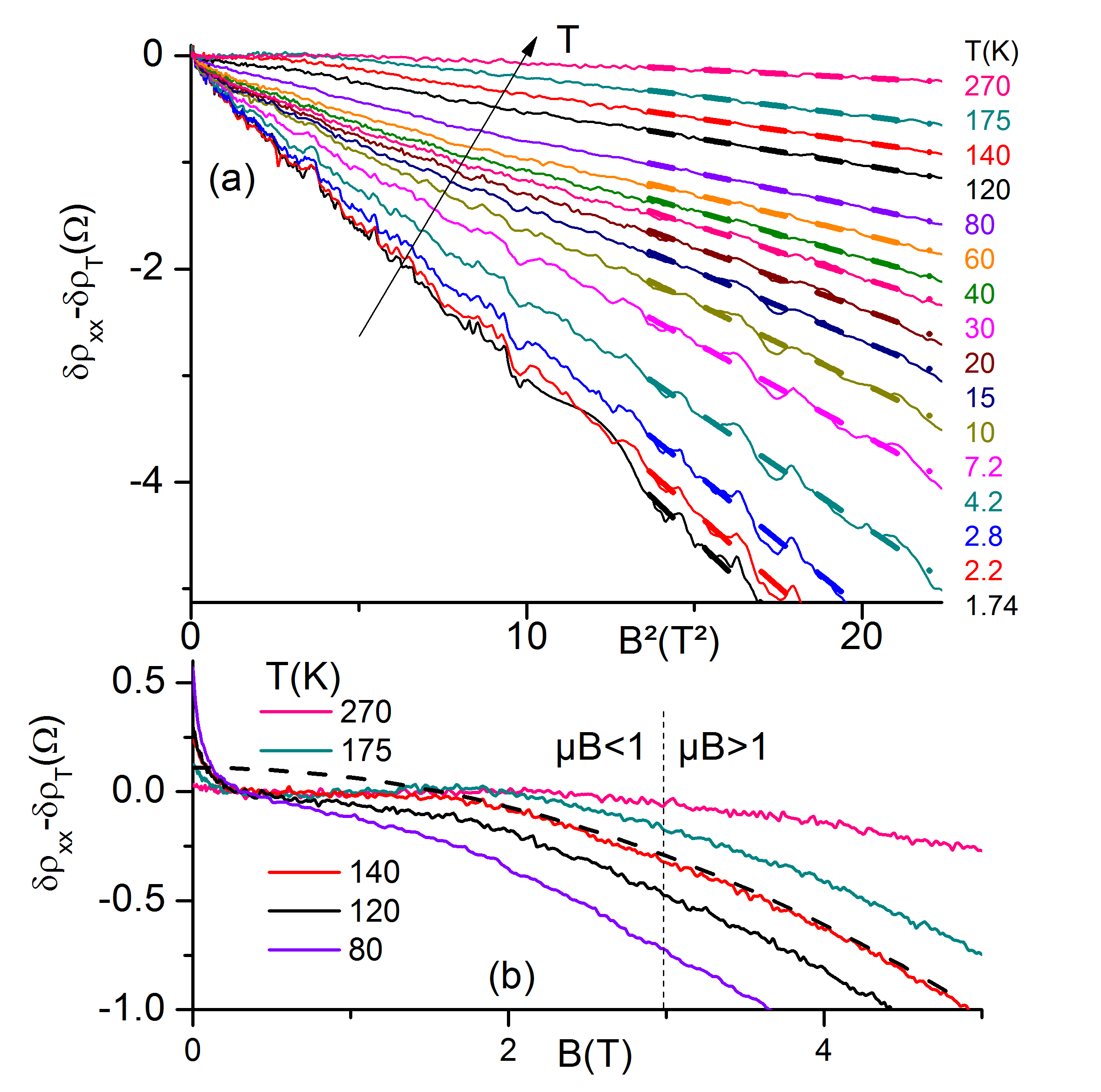
We can now extract the EEI correction at all temperatures, by subtracting the term from the magnetoresistivity , see Fig. 2. At ( K) and ( T), the corrected curves become flat, as shown in panel (b). This is one of the key features predicted in Ref. Gornyi and Mirlin (2004): when the ballistic regime is approached and the disorder is smooth, the parabolic EEI corrections are strongly suppressed at . For , EEI correction is preserved and all curves can be fitted by parabola. The fits are shown as thick dashed lines and their slopes give the dimensionless curvature :
| (5) |
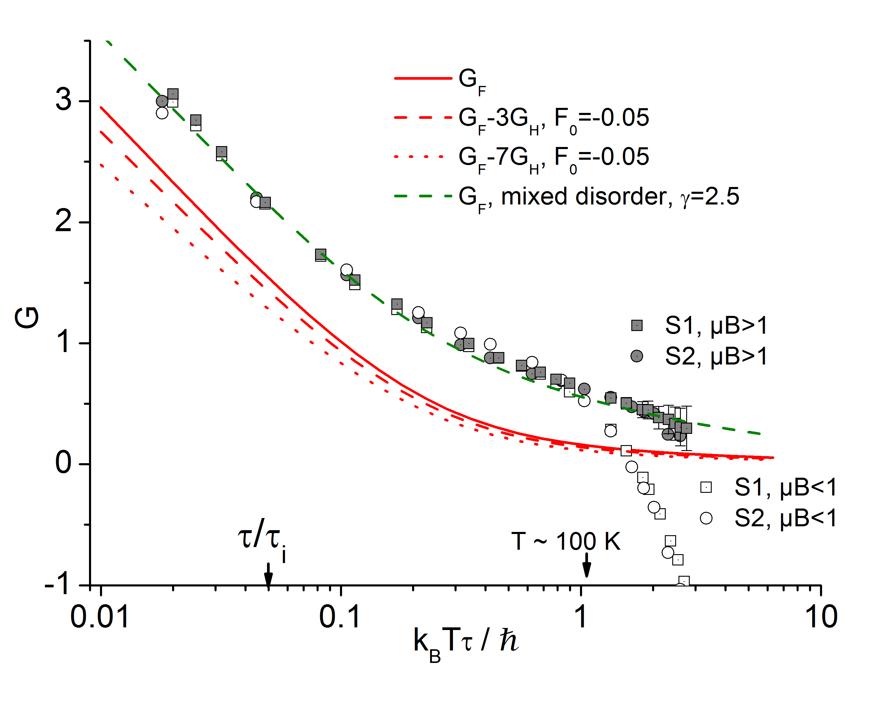
The curvature extracted from Fig. 2 is plotted in Fig. 3 for samples S1. The curvature of S2 is also indicated for comparison. The thermal correction plays a role only above . It then introduces uncertainties which are reported with error bars for sample S1. The raw MR coefficient at , without subtracting , is also plotted. The two coefficients at low and strong fields coincide at and diverge only at higher .
The theoretical curvature is given by , where is the exchange contribution, the Hartree contribution and the number of multiplet channels participating to the EEI. and are calculated following Ref. Gornyi and Mirlin (2004). The positive term can only reduce both the curvature and the slope of the bare term. The exchange term only, as plotted in Fig. 3, is already below the data points, with a slope in the diffusive regime similar to the experimental one. Therefore the Hartree term is too small to be detected in our experiments. This conclusion is reinforced by the constant slope observed around . In graphene is expected to change from 3 to 7 when exceeds and this should modify the curvature. Kozikov et al. (2010); Jobst et al. (2012) The corrections expected for and and are plotted in Fig. 3. depends on the Fermi liquid constant which is estimated by the formula: While this formula was first proposed in Ref. Kozikov et al. (2010) to explain low values of the experimental , it could still overestimate . Indeed, it gives for , a value which gives too small slopes with respect to the experimental data, see Fig. 3. The change of slope at is therefore attributed to the transition from the diffusive to the ballistic regime.
We comment now on the vertical shift observed in Fig. 3 between experiment and . In the case of mixed long range and short range disorders, the interaction induced curvature is increased by a factor , where is defined in Ref. Gornyi and Mirlin (2004) and is a prefactor which we take equal to , not , is the transport relaxation time of the smooth disorder only. From the best fit (green curve), we get . We assume that , where is the mean free time due to short range white noise potential and the factor 2 comes from the suppression of the backscattering due to the conservation of the pseudospin. This gives 100 fs with a corresponding length = 50 nm.
Another mechanism of classical origin can also increase the MR curvature Mirlin et al. (2001) and gives the observed amplitude of the observed MR for a mixed disorder situation. Li et al. (2003) However, this mechanism is temperature independent while experimentally decreases at high temperature, see Fig. 3.
IV.4 Raman
This distance is comparable to the distance between structural defects extracted from Raman spectroscopy. A typical Raman spectrum for sample S1 is presented in Fig. 4. To estimate the mean distance between the defects, we can calculate the intensity ratio of the and peaks which are observed in Raman spectroscopy. We then use the formula Cançado et al. (2011):
| (6) |
where is the energy of the laser beam in eV, and are the integrated intensities of the and bands respectively. The ratio is , which corresponds to an average distance nm.

IV.5 More extensive comparison with the litterature
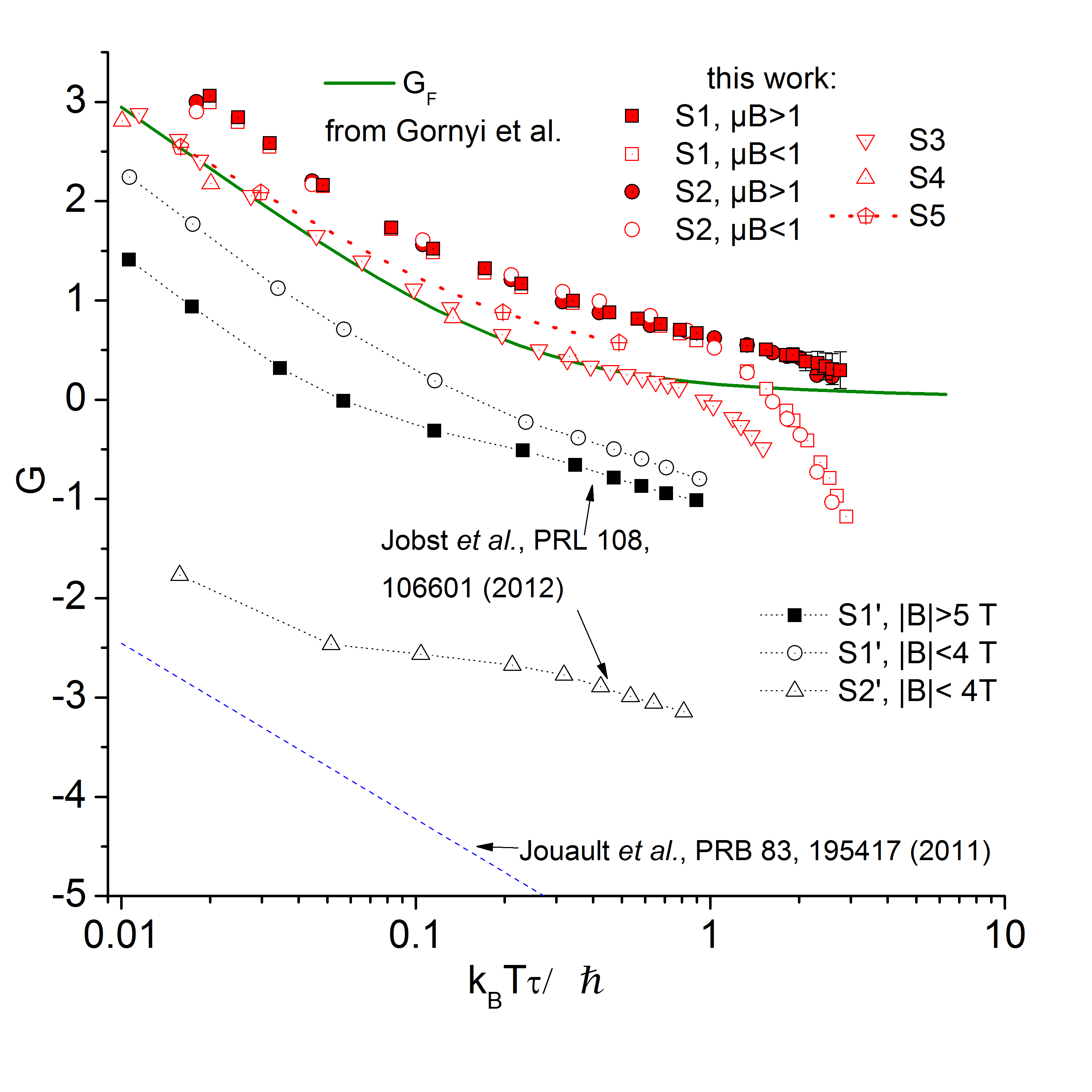
The magnetoresistances of the five samples S1-S5 have been studied and their curvatures are reported in Fig. 5. All samples have , with the exception of sample S3, for which . For samples S3, thermal averaging completely dominates the EEI correction at room temperature, on the whole magnetic field range. Samples S4 and S5 have been studied up to K only. A difference in the curvature below and above could be detected only for samples S1 and S2. For comparison, additional data taken from Ref. Jobst et al. (2012) and Jouault et al. (2011) are also reported in Fig. 5. The curve from Ref. Jouault et al. (2011) corresponds to an average of the two main samples studied in this reference.
All the curves in Fig. 5 are approximately identical. First, with the exception of the curve from Jouault et al. (2011), all curves in Fig. 5 have a change of their slopes around . For our samples, we attribute this change to the transition from the diffusive to the ballistic regime, as predicted by the theoretical curve.
Second, in the diffusive regime, the curves have the same slope for . However, they correspond to samples with different dielectric environment. In particular, samples from Ref. Jouault et al. (2011) are not covered by PMMA, while the samples of this work are. This should lead to variations of the slope via the Hartree term . Therefore, the influence of is probably too small to be detected. This in turn reinforces the attribution of the slope change to the diffusive-ballistic transition, and not to a modification of the number of multiplet channels participating to EEI.
Third, the curves differ mainly from the theoretical expectation by a vertical shift. Curves shifted downwards are probably prone to parasitic positive magnetoresistance induced for instance by current deflection or improper geometry. Curves shifted upwards are more intriguing. The enhanced negative curvature may result from the additional presence of short-range scatterers, as discussed previously.The very good agreement between and the theory is possibly fortuitous, as both parasitic PMR and NMR can be present and compensate for each other.
V conclusion
In conclusion, the magnetoresistance of monolayer graphene has been studied from 1.7 K to room temperature. The MR is well described by a recent theory of EEI valid for both diffusive and ballistic regimes. The overall enhanced negative curvature of the magnetoresistance points toward a situation of mixed disorder. This observation is sustained by additional Raman analysis. For graphene on SiC, the dominant scattering probably depends on the quality of the substrate. Finally, the dominance of short range scattering in our samples is in accordance with recent publications, where it is found that the mobility increases at low carrier density for epitaxial graphene. Farmer et al. (2011); Satrapinski et al. (2013)
VI Acknowledgement
We thank I. Gornyi for enlightening discussions. This work was partly supported by the ANR project MetroGraph ANR-2011-NANO-004-06.
References
- Geim (2011) A. K. Geim, Rev. Mod. Phys. 83, 851 (2011).
- Tikhonenko et al. (2008) F. V. Tikhonenko, D. W. Horsell, R. V. Gorbachev, and A. K. Savchenko, Phys. Rev. Lett. 100, 056802 (2008).
- Ponomarenko et al. (2009) L. A. Ponomarenko, R. Yang, T. M. Mohiuddin, M. I. Katsnelson, K. S. Novoselov, S. V. Morozov, A. A. Zhukov, F. Schedin, E. W. Hill, and A. K. Geim, Phys. Rev. Lett. 102, 206603 (2009).
- Monteverde et al. (2010) M. Monteverde, C. Ojeda-Aristizabal, R. Weil, K. Bennaceur, M. Ferrier, S. Guéron, C. Glattli, H. Bouchiat, J. N. Fuchs, and D. L. Maslov, Phys. Rev. Lett. 104, 126801 (2010).
- Guignard et al. (2012) J. Guignard, D. Leprat, D. C. Glattli, F. Schopfer, and W. Poirier, Phys. Rev. B 85, 165420 (2012).
- Kozikov et al. (2010) A. A. Kozikov, A. K. Savchenko, B. N. Narozhny, and A. V. Shytov, Phys. Rev. B 82, 075424 (2010).
- Jouault et al. (2011) B. Jouault, B. Jabakhanji, N. Camara, W. Desrat, C. Consejo, and J. Camassel, Phys. Rev. B 83, 195417 (2011).
- Jobst et al. (2012) J. Jobst, D. Waldmann, I. V. Gornyi, A. D. Mirlin, and H. B. Weber, Phys. Rev. Lett. 108, 106601 (2012).
- Iagallo et al. (2013) A. Iagallo, S. Tanabe, S. Roddaro, M. Takamura, H. Hibino, and S. Heun, Phys. Rev. B 88, 235406 (2013).
- Altshuler and Aronov (1985) B. L. Altshuler and A. G. Aronov, Electron-Electron Interactions Disordered Systems Modern Problems in Condensed Matter Science (North-Holland, Amsterdam, 1985).
- Bergmann (1984) G. Bergmann, Weak localization in thin films (1984).
- Mirlin et al. (2001) A. D. Mirlin, D. G. Polyakov, F. Evers, and P. Wölfle, Phys. Rev. Lett. 87, 126805 (2001).
- Polyakov et al. (2001) D. G. Polyakov, F. Evers, A. D. Mirlin, and P. Wölfle, Phys. Rev. B 64, 205306 (2001).
- Minkov et al. (2003) G. M. Minkov, O. E. Rut, A. V. Germanenko, A. A. Sherstobitov, V. I. Shashkin, O. I. Khrykin, and B. N. Zvonkov, Phys. Rev. B 67, 205306 (2003).
- Goh et al. (2008) K. E. J. Goh, M. Y. Simmons, and A. R. Hamilton, Phys. Rev. B 77, 235410 (2008).
- Zala et al. (2001) G. Zala, B. N. Narozhny, and I. L. Aleiner, Phys. Rev. B 64, 214204 (2001).
- Pudalov et al. (2003) V. M. Pudalov, M. E. Gershenson, H. Kojima, G. Brunthaler, A. Prinz, and G. Bauer, Phys. Rev. Lett. 91, 126403 (2003).
- Shashkin et al. (2002) A. A. Shashkin, S. V. Kravchenko, V. T. Dolgopolov, and T. M. Klapwijk, Phys. Rev. B 66, 073303 (2002).
- Coleridge et al. (2002) P. T. Coleridge, A. S. Sachrajda, and P. Zawadzki, Phys. Rev. B 65, 125328 (2002).
- Proskuryakov et al. (2002) Y. Y. Proskuryakov, A. K. Savchenko, S. S. Safonov, M. Pepper, M. Y. Simmons, and D. A. Ritchie, Phys. Rev. Lett. 89, 076406 (2002).
- Peres (2010) N. M. R. Peres, Rev. Mod. Phys. 82, 2673 (2010).
- Gornyi and Mirlin (2004) I. V. Gornyi and A. D. Mirlin, Phys. Rev. B 69, 045313 (2004).
- Cheianov and Fal’ko (2006) V. V. Cheianov and V. I. Fal’ko, Phys. Rev. Lett. 97, 226801 (2006).
- Michon et al. (2010) A. Michon, S. Vezian, A. Ouerghi, M. Zielinski, T. Chassagne, and M. Portail, Appl. Phys. Lett. 97, 171909 (2010).
- Michon et al. (2013) A. Michon, S. Vezian, E. Roudon, D. Lefebvre, M. Zielinski, T. Chassagne, and M. Portail, J. Appl. Phys. 113, 203501 (2013).
- Riedl et al. (2009) C. Riedl, C. Coletti, T. Iwasaki, A. A. Zakharov, and U. Starke, Phys. Rev. Lett. 103, 246804 (2009).
- Jabakhanji et al. (2014) B. Jabakhanji, A. Michon, C. Consejo, W. Desrat, M. Portail, A. Tiberj, M. Paillet, A. Zahab, F. Cheynis, F. Lafont, et al., Phys. Rev. B 89, 085422 (2014).
- Li et al. (2003) L. Li, Y. Y. Proskuryakov, A. K. Savchenko, E. H. Linfield, and D. A. Ritchie, Phys. Rev. Lett. 90, 076802 (2003).
- Kechedzhi et al. (2007) K. Kechedzhi, E. McCann, V. I. Fal’ko, H. Suzuura, T. Ando, and B. L. Altshuler, The European Physical Journal Special Topics 148, 39 (2007), ISSN 1951-6355.
- Kuntsevich et al. (2009) A. Y. Kuntsevich, G. M. Minkov, A. A. Sherstobitov, and V. M. Pudalov, Phys. Rev. B 79, 205319 (2009).
- Sedrakyan and Raikh (2008) T. A. Sedrakyan and M. E. Raikh, Phys. Rev. Lett. 100, 106806 (2008).
- Mirlin et al. (1999) A. D. Mirlin, J. Wilke, F. Evers, D. G. Polyakov, and P. Wölfle, Phys. Rev. Lett. 83, 2801 (1999).
- Das Sarma et al. (2011) S. Das Sarma, S. Adam, E. H. Hwang, and E. Rossi, Rev. Mod. Phys. 83, 407 (2011).
- Alekseev et al. (2013) P. S. Alekseev, A. P. Dmitriev, I. V. Gornyi, and V. Y. Kachorovskii, Phys. Rev. B 87, 165432 (2013).
- Hwang and Das Sarma (2008) E. H. Hwang and S. Das Sarma, Phys. Rev. B 77, 115449 (2008).
- Fratini and Guinea (2008) S. Fratini and F. Guinea, Phys. Rev. B 77, 195415 (2008).
- Ray et al. (2012) N. Ray, S. Shallcross, S. Hensel, and O. Pankratov, Phys. Rev. B 86, 125426 (2012).
- (38) The value of has been determined to adapt the formula proposed in Ref. 22 to low values of .
- Cançado et al. (2011) L. G. Cançado, A. Jorio, E. H. M. Ferreira, F. Stavale, C. A. Achete, R. B. Capaz, M. V. O. Moutinho, A. Lombardo, T. S. Kulmala, and A. C. Ferrari, Nano Letters 11, 3190 (2011), eprint http://pubs.acs.org/doi/pdf/10.1021/nl201432g.
- Farmer et al. (2011) D. B. Farmer, V. Perebeinos, Y.-M. Lin, C. Dimitrakopoulos, and P. Avouris, Phys. Rev. B 84, 205417 (2011).
- Satrapinski et al. (2013) A. Satrapinski, S. Novikov, and N. Lebedeva, Applied Physics Letters 103, 173509 (2013).
- Lifshitz and Kosevich (1956) I. M. Lifshitz and A. M. Kosevich, Sov. Phys. JETP 2, 636 (1956).
- Gusynin and Sharapov (2005) V. P. Gusynin and S. G. Sharapov, Phys. Rev. B 71, 125124 (2005).
VII Appendix: fits of the SdH oscillations
We fitted the SdH oscillations of the samples using the Lifshitz-Kosevich Lifshitz and Kosevich (1956); Gusynin and Sharapov (2005) formula in which only the first harmonic is retained:
| (7) |
Here is the Dingle factor: , is temperature amplitude factor: with =; is the quantum time, is the Fermi energy, is the cyclotron frequency, is the cyclotron mass, is a phase factor and an integer. The phase determines the nature of the carriers. For a graphene layer: and . For two dimensional massive carriers: and . For three dimensional massive carriers, and .
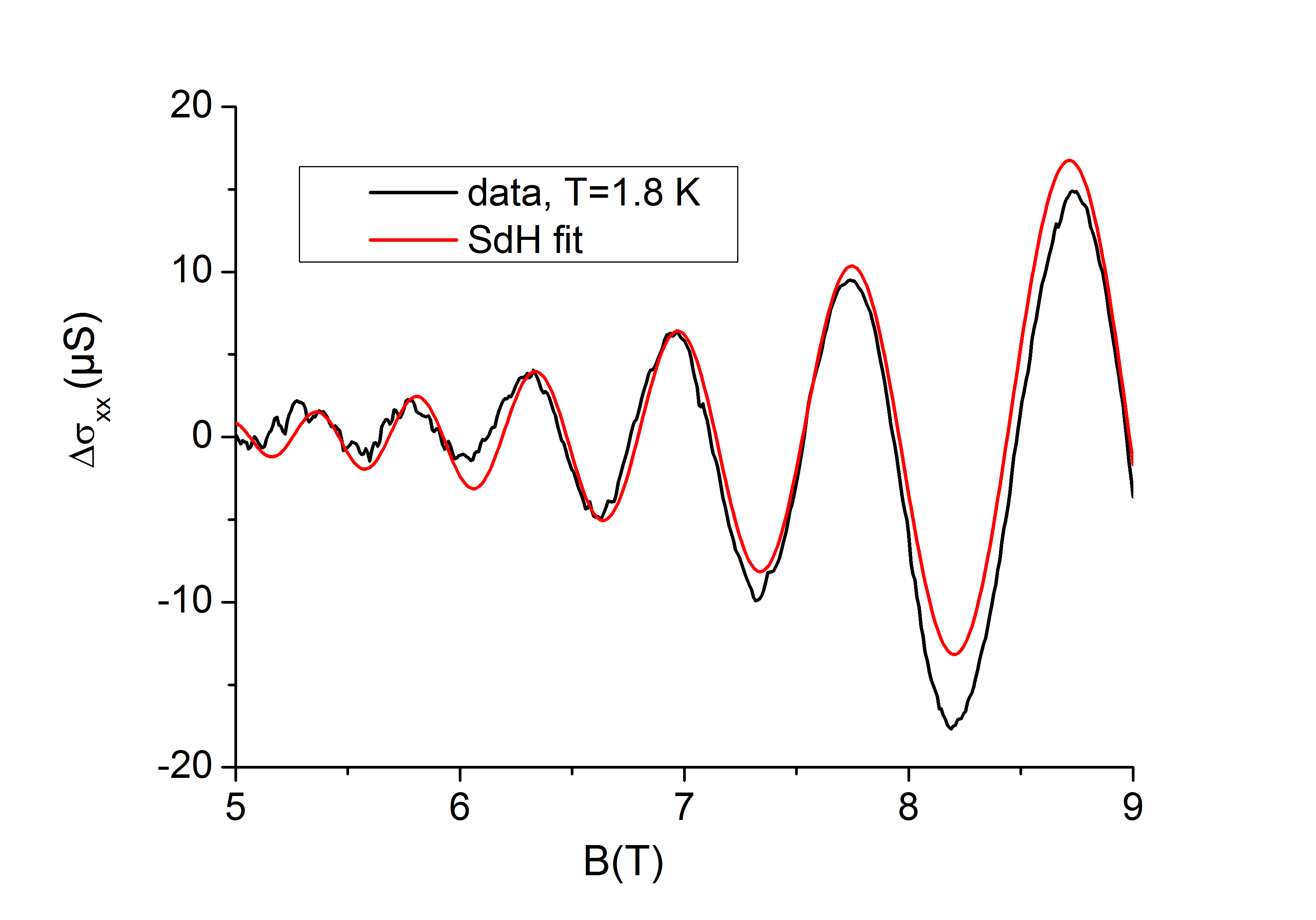
The best fit for sample at = 1.7 K is reported in Fig. 6. It gives and 17 fs.