Spin-helical Dirac states in graphene induced by polar-substrate surfaces with giant spin-orbit interaction: a new platform for spintronics
Abstract
Spintronics, or spin electronics, is aimed at efficient control and manipulation of spin degrees of freedom in electron systems. To comply with demands of nowaday spintronics, the studies of electron systems hosting giant spin-orbit-split electron states have become one of the most important directions providing us with a basis for desirable spintronics devices. In construction of such devices, it is also tempting to involve graphene, which has attracted great attention because of its unique and remarkable electronic properties and was recognized as a viable replacement for silicon in electronics. In this case, a challenging goal is to make graphene Dirac states spin-polarized. Here, we report on absolutely new promising pathway to create spin-polarized Dirac states based on coupling of graphene and polar-substrate surface states with giant Rashba-type spin-splitting. We demonstrate how the spin-helical Dirac states are formed in graphene deposited on the surface of BiTeCl. This coupling induces spin separation of the originally spin-degenerate graphene states and results in fully helical in-plane spin polarization of the Dirac electrons.
pacs:
73.20.-r, 79.60.-iI Introduction
Graphene is a fascinating material, which has attracted great attention because of its unique electronic properties GN_NatMat2007 ; Castro_RevModPhys2009 . In graphene spintronics, many efforts were made to realize a robust control of electron spins by, e.g., magnetoelectric coupling or spin-orbit interaction (SOI) Zutic_RevModPhys2004 ; Awschalom_NatPhys2007 ; Zhang_PRL2009 . Main hopes were pinned on the SOI effect, which can be directly observed Kato_Sci2004 ; Wunderlich_PRL2005 .
Some interesting phenomena, such as quantum spin Hall effect KaneMele_PRL2005 , quantum anomalous Hall effect Qiao_PRB2010 , and other phenomena were predicted in graphene. However, the intrinsic spin-orbit splitting in pristine graphene is proved to be too weak to produce an observable effect and to realize practical applications KaneMele_PRL2005 ; Yao_PRB2007 ; Gmitra_PRB2009 . The major challenge in graphene spintronics is to make graphene Dirac states spin-polarized. In principle, it can be realized by applying an extrinsic SOI, i.e., by placing the grapnene in a proper medium with a strong spin-orbit coupling. Numerous previous works, both experimental and theoretical, have been aimed at enhancement of graphene SOI via adatoms deposition Castro_PRL2009 ; Abdelouahed_PRB2010 ; Qiao_PRB2010 ; Weeks_PRX or growth of graphene on metal substrates Dedkov_PRL2008 ; Varykhalov_PRL2008 ; Heer_JPhD2010 ; Li_JPCM2011 ; Marchenko_NatCom2012 .
In the present paper, we propose a new pathway to manipulate the electronic and spin properties of graphene by its depositing on a polar-substrate surface possessing a giant Rashba-type spin-split surface state. We state that one of the efficient mechanisms responsible for appearance of spin-polarised Dirac states in graphene is the coupling of two two-dimensional (2D) electron systems: Dirac electrons of graphene and Rashba electrons of the mentioned surface state. To corroborate our statement, we have chosen the most suitable 2D Rashba-electron system formed by electons in the surface state at the Te-terminated surface of bismuth tellurohalides. Here, on the base of relativistic density functional theory (DFT) calculations, we show that graphene deposited on BiTeCl is the system with unique electronic properties, in which the strong hybridization of Dirac and Rashba electrons gives rise to spin-helical Dirac states.
II Method
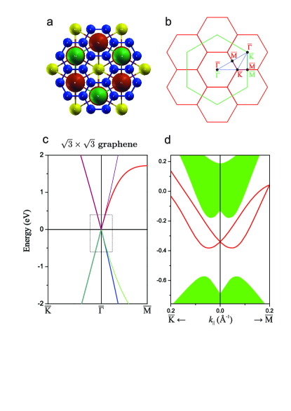
Our calculations were based on DFT as implemented in the Vienna ab initio simulation package VASP, VASP1 ; VASP2 . The generalized gradient approximation (GGA) of Perdew, Burke, and Ernzerhof (PBE) GGA_PBE to the exchange correlation (XC) potential has been implemented. The interaction between the ion cores and valence electrons was described by the projector augmented-wave method PAW1 ; PAW2 . The Hamiltonian contained the scalar relativistic corrections, and the spin-orbit coupling was taken into account by the second variation method Koelling . To simulate BiTeCl substrate we consider a 24 atomic layer slab. Hydrogen monolayer was used to passivate the chlorine side of the slab as was described in Ref. Eremeev_PRL . The positions of atoms in the graphene layer and within three outermost atomic layers of the BiTeCl slab were optimized including SOI self-consistently. The distance between the substrate and the graphene layer was found to be of Å. The atoms of the deeper layers were kept fixed at the bulk crystalline positions. The -point mesh of was used for the Brillouin zone of the surface unit cell.
III Results
Recently, it was shown that the Te-terminated surface of non-centrosymmetric hexagonal-structured polar-semiconductor compounds BiTe(Cl,Br,I) meet requirements for spintronics applications, since these systems hold a giant Rashba spin splitting of a free-electron-like surface state at the point Eremeev_PRL ; Crepaldi_PRL ; Landolt_PRL ; Eremeev_JETPlett ; Sakano ; Eremeev_NJP . The mentioned bismuth tellurohalides are characterized by ionic bonding with large charge transfer from bismuth to halide- and tellutium-atomic layers. The spin-split surface states at the Te-terminated surface emerge by splitting off from the lowest conduction band, owing to the decreasing potential within the near-surface layers Eremeev_PRL , which is a consequence of strong ionicity. One can expect that deposition of graphene on BiTe(Cl,Br,I), can result in a strong interaction and hybridization of the Rashba and Dirac 2D electrons. In designing such systems, it is important to match the lattice parameters of the contacting materials. The in-plane hexagonal parameter of BiTeCl matches perfectly with the parameter of graphene. Thus, the deposited graphene should not undergo the in-plane strain [Fig. 1(a)]. In the structure, the Brillouin zone of graphene takes a third of the original one [Fig. 1(b)]. Under this folding, the -point Dirac cone of graphene appears as four-fold degenerate state [Fig. 1(c)] with linear dispersion in the vicinity of the Dirac point (Fig. 1(c), the dotted-line rectangle). Thus, both the Dirac state and the Rashba state of the pristine substrate [Fig. 1(d)] reside in the Brillouin zone center.
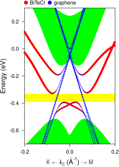
The interaction of the two 2D electron systems results in a strong modification of the spectra with respect to the constituents (Fig. 2). In the upper part of the gap, at large the Rashba states of BiTeCl are preserved, while at Å-1 both inner and outer branches of the Rashba states rapidly become strongly hybridized with graphene cone states, and already at Å-1 they are completely localized within the graphene layer, dispersing towards the Dirac point, which is immersed in the conduction band of the substrate bulk states. In the lower part of the gap, two of four graphene bands are hybridized with the substrate forming hole-like Rashba state near the valence band, which is completely localized within substrate layers in the vicinity of the point. Thus, hybridization of two graphene branches with the Rashba state of the BiTeCl substrate leads to a break of both branches of the Rashba states at small in such a way that its degeneracy point appears near the valence band or, to the contrary, the Rashba states break two graphene branches. Other two Dirac branches remain unchanged and localized in the graphene layer for all . As a result of these changes, in the middle part of the bulk band gap within the energy interval of 70 meV (see yellow stripe in Fig. 2) two almost degenerate Dirac states of graphene survive. The small SOI-induced -splitting for the Dirac cones is less then 0.002 Å-1.
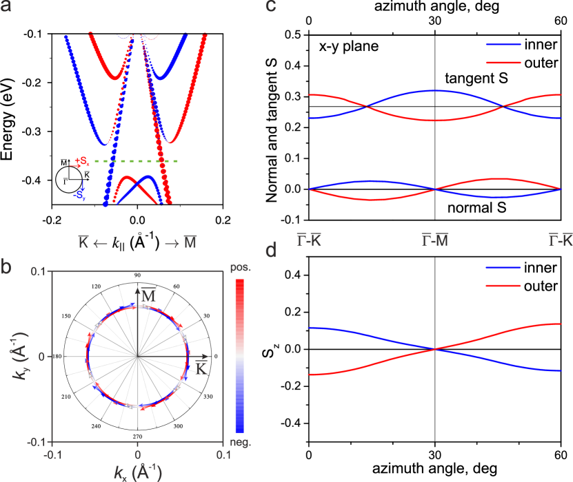
The spin structure of the surface states within the band gap is shown in Fig. 3(a). As seen in the figure, at large the Rashba branches preserve the spin polarization of the clean Te-terminated BiTeCl surface: they demonstrate counter-clockwise and clockwise in-plane helicity for the inner and outer branches, respectively. At Å-1, where due to hybridization the Rashba branches turn into the Dirac states and start to be localized at the graphene layer, the spin helicity of the graphene band hybridizing with the outer branch becomes the same as that of the inner branch. Consequently, both hybridized graphene bands have the counter-clockwise spin polarization. It certainly would mean that two remaining non-hybridized Dirac bands should be characterized by the clockwise spin polarization, as it is confirmed by the spin-resolved bands presented in Fig. 3(a). Thus, and this is the main issue of the present study, the hybridization between the graphene and substrate-Rashba-split 2D electrons provides the helical spin separation of the graphene Dirac states.
As was mentioned above, the most interesting feature of the graphene@BiTeCl spectrum is the energy window of 70 meV width, where the Dirac states of graphene exist only (see yellow stripe in Fig. 2). The two almost degenerate Dirac states have the same in-plane spin polarization, which can be clearly seen in Fig. 3(b), where spin-resolved constant energy contours in the middle of this energy window are shown. Both Dirac states, apart from the in-plane clockwise spin polarization, also demonstrate the presence of the out-of-plane spin component, which is intrinsic feature of the spin-polarized states at hexagonal surfaces. The detailed spin texture is illustrated in Figs. 3(c) and (d). Fig. 3(c) shows the azimuthal dependencies of the in-plane spin components in the tangent and normal directions to the inner and outer Dirac contours. One can see that the tangent component for both bands demonstrates variation around the value of 0.27, while the normal component experiences small variations near zero spin value. For both bands, the out-of-plane spin component [Fig. 3(d)] also varies near zero but the variations are significantly larger than those for the normal component. Nevertheless, the maximal out-of-plane spin values, which are observed along the directions, are three times smaller than the magnitude of the tangent in-plane spin component. Furthermore, the signs of both normal and out-of-plane spin components are opposite for the inner and outer almost degenerate Dirac contours, what results in a fully helical net in-plane spin polarization of the Dirac electrons.
IV Discussion
Apparently, the revealed possibility to create the helical spin-polarized Dirac electrons in graphene opens up new horizons in the graphene-based spintronics. The mentioned spin texture of the graphene Dirac states is important to come out as a consequence of the strong hybridization between graphene and giant Rashba-split states of the Te-terminated surface of the polar substrate BiTeCl. Due to excellent matching lattice parameters of BiTeCl and graphene, the graphene@BiTeCl system can be easily realized on practice. The reported energy interval of meV in the middle part of the projected bulk energy gap, where the spin-polarized Dirac states solely exist, is sufficiently enough for spintronics applications. However, it should be noted that this energy interval can be wider in a real system, since the band gap is normally underestimated within the DFT. As shown both by experiment Sakano and by the bulk calculations Rusinov , the bulk band gap in BiTeCl is a factor of two larger than that predicted by the DFT. In order to actively bring the spin-polarized Dirac states located in the middle part of the gap into play, the chemical potential of the system should be decreased by meV with respect to the Fermi level obtained in the present calculation. The chemical potential tuning can be realized by applying electric field or doping hole-donating adsorbates. The latter approach seems to be preferable. As was recently shown for Au/Si system, supporting Rashba-split surface state, the Fermi level position can be effectively tuned within the range of meV by choosing appropriate adsorbate species Bondarenko .
Except the spin-polarized Dirac states in the middle part of the gap, the surface states in upper and lower parts of the bulk gap may also be of considerable interest, because in the respective energy regions the helical Dirac states of graphene and Rashba spin-split states coexists. Various intriguing physical phenomena related to decay of elementary excitations in the states with different velocities can be expected.
We believe that our findings will stimulate further theoretical and experimental investigations of spin-polarized Dirac fermions which is a key matter for prospective spintronics applications.
V acknowledgements
We acknowledge partial support from the Basque Country Government, Departamento de Educación, Universidades e Investigación (Grant No. IT-756-13), the Spanish Ministerio de Ciencia e Innovación (Grant No. FIS2010-19609-C02-01), and the Ministry of Education and Science of Russian Federation (Grant No. 2.8575.2013).
References
- (1) A. K. Geim, K. S. Novoselov, Nat. Mater 6, 183 (2007).
- (2) A. H. Castro Neto, F. Guinea, N. M. R. Peres, K. S. Novoselov, A. K. Geim, Rev. Mod. Phys. 81, 109 (2009).
- (3) I. Žutić, J. Fabian, S. Das Sarma, Rev. Mod. Phys. 76, 323 (2004).
- (4) D. D. Awschalom, M. E. Flatte, Nat. Phys 3, 153 (2007).
- (5) Z. Zhang, C. Chen, W. Guo, Phys. Rev. Lett. 103, 187204 (2009).
- (6) Y. K. Kato, R. C. Myers, A. C. Gossard, D. D. Awschalom, Science 306, 1910 (2004).
- (7) J. Wunderlich, B. Kaestner, J. Sinova, T. Jungwirth, Phys. Rev. Lett. 94, 047204 (2005).
- (8) C. L. Kane, E. J. Mele, Phys. Rev. Lett. 95, 226801 (2005).
- (9) Z. Qiao, S. A. Yang, W. Feng, W.-K. Tse, J. Ding, Y. Yao, et al., Phys. Rev. B 82, 161414 (2010).
- (10) Y. Yao, F. Ye, X.-L. Qi, S.-C. Zhang, Z. Fang, Phys. Rev. B 75, 041401 (2007).
- (11) M. Gmitra, S. Konschuh, C. Ertler, C. Ambrosch-Draxl, J. Fabian, Phys. Rev. B 80, 235431 (2009).
- (12) A. H. Castro Neto and F. Guinea, Phys. Rev. Lett. 103, 026804 (2009).
- (13) S. Abdelouahed, A. Ernst, J. Henk, I.V. Maznichenko, and I. Mertig, Phys. Rev. B 82, 125424 (2010).
- (14) C. Weeks, J. Hu, J. Alicea, M. Franz, and R. Wu, Phys. Rev. X 1, 021001 (2011).
- (15) Yu. S. Dedkov, M. Fonin, U. Rüdiger, and C. Laubschat, Phys. Rev. Lett. 100, 107602 (2008).
- (16) A. Varykhalov, J. Saánchez-Barriga, A. M. Shikin, C. Biswas, E. Vescovo, A. Rybkin, D. Marchenko, and O. Rader, Phys. Rev. Lett. 101, 157601 (2008).
- (17) W. A. de Heer, C. Berger, X. Wu, M. Sprinkle, Y. Hu, M. Ruan, J. A. Stroscio, Ph. N. First, R. Haddon, B. Piot, C. Faugeras, M. Potemski, and J.-S. Moon, J. Phys. D: Appl. Phys. 43, 374007 (2010).
- (18) Z. Y. Li, Z. Q. Yang, S. Qiao, J. Hu, R. Q. Wu, J. Phys.: Condens. Matter 23, 225502 (2011).
- (19) D. Marchenko, A. Varykhalov, M. R. Scholz, G. Bihlmayer, E. I. Rashba, A. Rybkin, A. M. Shikin, and O. Rader, Nature Commun. 6, 1232 (2012).
- (20) S. V. Eremeev, I. A. Nechaev, Yu. M. Koroteev, P. M. Echenique, and E. V. Chulkov, Phys. Rev. Lett. 108, 246802 (2012).
- (21) A. Crepaldi, L. Moreschini, G. Auteè, C. Tournier-Colletta, S. Moser, N. Virk, H. Berger, Ph. Bugnon, Y. J. Chang, K. Kern, A. Bostwick, E. Rotenberg, O. V. Yazyev, and M. Grioni, Phys. Rev. Lett. 109, 096803 (2012).
- (22) G. Landolt, S. V. Eremeev, Y. M. Koroteev, B. Slomski, S. Muff, T. Neupert, M. Kobayashi, V. N. Strocov, T. Schmitt, Z. S. Aliev, M. B. Babanly, I. R. Amiraslanov, E. V. Chulkov, J. Osterwalder, and J. H. Dil, Phys. Rev. Lett. 109, 116403 (2012).
- (23) S. V. Eremeev, A. I. Nechaev, E. V. Chulkov, JETP Lett. 96, 437 (2012).
- (24) M. Sakano, M. S. Bahramy, A. Katayama, T. Shimojima, H. Murakawa, Y. Kaneko, W. Malaeb, S. Shin, K. Ono, H. Kumigashira, R. Arita, N. Nagaosa, H. Y. Hwang, Y. Tokura, and K. Ishizaka, Phys. Rev. Lett. 110, 107204 (2013).
- (25) S. V. Eremeev, I. P. Rusinov, A. I. Nechaev, E. V. Chulkov, New J. Phys. 15, 075015 (2013).
- (26) I. P. Rusinov, I. A. Nechaev, S. V. Eremeev, C. Friedrich, S. Blügel, and E. V. Chulkov, Phys. Rev. B 87, 205103 (2013).
- (27) L. V. Bondarenko, D. V. Gruznev, A. A. Yakovlev, A. Y. Tupchaya, D. Usachov, O. Vilkov, A. Fedorov, D. V. Vyalikh, S. V. Eremeev, E. V. Chulkov, A. V. Zotov, and A. A. Saranin, Scientific Reports 3, 1826 (2013).
- (28) G. Kresse, J. Hafner, Phys. Rev. B 48, 13115 (1993).
- (29) G. Kresse, J. Furthmüller, Comput. Mater. Sci. 6, 15 (1996).
- (30) J.P. Perdew, K. Burke, and M. Ernzerhof, Phys. Rev. Lett. 77, 3865 (1996); J.P. Perdew, K. Burke, and M. Ernzerhof, Phys. Rev. Lett. 78, 1396(E) (1997).
- (31) P.E. Blöchl, Phys. Rev. B 50, 17953 (1994).
- (32) G. Kresse, D. Joubert, Phys. Rev. B 59, 1758 (1999).
- (33) D.D. Koelling, B.N. Harmon, J. Phys. C 10, 3107 (1977).