Interplay between Mn-acceptor state and Dirac surface states in Mn-doped Bi2Se3 topological insulator
Abstract
We investigate the properties of a single substitutional Mn impurity and its associated acceptor state on the (111) surface of Bi2Se3 topological insulator. Combining ab initio calculations with microscopic tight-binding modeling, we identify the effects of inversion-symmetry and time-reversal-symmetry breaking on the electronic states in the vicinity of the Dirac point. In agreement with experiments, we find evidence that the Mn ion is in the -valence state and introduces an acceptor in the bulk band gap. The Mn-acceptor has predominantly –character, and is localized mainly around the Mn impurity and its nearest-neighbor Se atoms. Its electronic structure and spin-polarization are determined by the hybridization between the Mn –levels and the –levels of surrounding Se atoms, which is strongly affected by electronic correlations at the Mn site. The opening of the gap at the Dirac point depends crucially on the quasi-resonant coupling and the strong real-space overlap between the spin-chiral surface states and the mid-gap spin-polarized Mn-acceptor states.
pacs:
73.20.Hb, 73.20.At, 71.15.-m,I INTRODUCTION
Topological insulators (TIs), characterized by a non-trivial insulating gap
in the bulk and topologically protected helical states on the
boundaries, are a new frontier
in condensed matter physics and materials science Hasan and Kane (2010); Qi and Zhang (2011).
Topological surface states (TSSs) in three-dimensional (3D) TIs,
such as the Bi2Se3 family with a single Dirac cone,
have attracted particular attention Zhang et al. (2009).
While the TSSs are robust against time-reversal-invariant
perturbations, the breaking of time-reversal symmetry (TRS)
opens up an energy gap at the Dirac point. One way to explore
the response of the TSSs to TRS breaking is via magnetic ordering.
Apart from being a prerequisite for future spintronic applications,
the presence of magnetic order in 3D TIs manifests itself in novel quantum phenomena,
such as the quantum anomalous Hall effect Yu et al. (2010); Chang et al. (2013)
and the topological
magnetoelectric effect Qi et al. (2008).
A finite density of magnetic impurities
on a 3D TI surface
is expected to bring about a gapped magnetic phase, with magnetic moments
coupled by a surface-state-mediated exchange
interaction Liu et al. (2009); Checkelsky et al. (2012),
similar to the carrier-mediated exchange
coupling in dilute magnetic semiconductors (DMSs).
However, before one can identify the nature of magnetic interactions,
it is critical to understand the physics of individual magnetic dopants both in bulk and near
the surface of a 3D TI.
To date, there seems to be no consensus
in experimental and theoretical literature
on the behavior of different species of magnetic impurities in these systems.
Contrasting results have been reported regarding the chemical trends
and the magnetic state of the
impurities Niu et al. (2011); Henk et al. (2012a); Abdalla et al. (2013); Li et al. (2014), as well
as the presence or absence of the energy gap at the Dirac point upon
doping Chen et al. (2010); Scholz et al. (2012); Valla et al. (2012); Honolka et al. (2012); Schmidt et al. (2013).
For instance, scanning tunneling spectroscopy (STM) and angular resolved photoemission
spectroscopy (ARPES) experiments on Bi2Se3 family of 3D TIs
have demonstrated the opening of the gap by doping with Fe and Mn Chen et al. (2010); Wray et al. (2011); Hor et al. (2010); Xu et al. (2012).
However, more recent work reported striking robustness of the TSS in the
presence of magnetic dopants, such as Fe, Co and Gd Scholz et al. (2012); Honolka et al. (2012); Shelford et al. (2012); Valla et al. (2012).
Theoretical results also differ, with some density functional theory (DFT) calculations confirming the presence of the gap
at the Dirac point Li et al. (2012); Zhang et al. (2012); Henk et al. (2012b); Schmidt et al. (2011) and others suggesting different scenarios,
including a shift at the Dirac cone from the center of the Brillouin zone, Honolka et al. (2012); Henk et al. (2012a)
as well as strong dependence on the magnetization orientation and valence state across the transition-metal (TM) series Abdalla et al. (2013).
We should also note that there exist other possible mechanisms for magnetic ordering in 3D TI systems, different from
the carrier-mediated (RKKY) interaction Liu et al. (2009); Biswas and Balatsky (2010); Abanin and Pesin (2011); Efimkin and Galitski (2014) typical of DMSs.
It is known that in Bi2Se3 both the conduction and valence bands are formed by -orbitals and
that the spin-orbit interaction is strong, resulting in band inversion and an energy gap in the bulk. This leads to large matrix elements
of the spin-operator between the wave functions of conduction and valence bands and, as a consequence, to a large Van Vleck spin susceptibility Yu et al. (2010).
In contrast to DMSs, where this effect is usually small, in the Bi2Se3 family of 3D TIs this can lead to a ferromagnetic order even if the dopants
do not introduce free carriers into the host material such as Fe dopants.
Hence, possible mechanisms for magnetic interactions may vary depending on the nature of magnetic dopants and
different dopant species must be carefully examined.
For the important case of magnetic acceptors,
e.g. Mn on (111) Bi2Se3 surface, a detailed
microscopic description,
consistent with experimental observations,
is lacking.
There is a strong experimental evidence that Mn behaves
as a substitutional acceptor
in the Bi2Se3 family of 3D
TIs Hor et al. (2010); Choi et al. (2013); Janíček et al. (2008).
Typically, Mn substitutes Bi in Bi2Se3 in
the configuration, corresponding to the valence state,
giving rise to a spin .
Since the nominal valence of Bi is ,
this implies that substitutional Mn
impurities also introduce acceptor (hole) states in the
bulk gap of the host material, similarly to Mn in GaAs, a typical DMS.
These acceptor levels can be directly probed by STM Hor et al. (2010).
However, the nature of these states and their interplay with
the Dirac surface states
have not yet been analyzed theoretically.
In this work we investigate single substitutional Mn impurities
on the (111) surface of Bi2Se3, using
DFT and tight-binding (TB) models.
We find that
Mn+2 introduces a mid-gap acceptor state,
localized mainly on the impurity and
the nearest-neighbor (NN) Se atoms,
similar to a substitutional Mn in GaAs Mahani et al. (2014).
Our calculations demonstrate the importance
of electronic
correlations at the impurity site, which we model by a Hubbard
parameter Anisimov et al. (1991).
The parameter controls the position of the
impurity –orbitals, which in turn determines the hybridization
with the –orbitals of NN Se atoms and the acceptor spin-polarization.
Increasing
localizes the Mn –states, leading to an enhancement
in the Mn magnetic moment and a weakening of the – hybridization
and the acceptor polarization.
With the Mn placed on one of the surfaces of a finite slab,
the spin-polarized acceptor states
couple quasi-resonantly with the helical TSS at the same surface,
opening a gap of a few meV at the Dirac point. The magnitude of
the gap is significantly affected by
the strength of the – hybridization.
With the appearance of the energy gap,
the system exhibits a finite out-of-plane
magnetization Liu et al. (2009); Checkelsky et al. (2012).
The rest of the paper is organized as follows.
In Section II we discuss the details of the DFT
calculations and the TB model for magnetic and nonmagnetic impurities in Bi2Se3.
The results of DFT and TB calculations are presented in
Section III. In particular, we describe
modifications in the electronic bandstructure of a
Bi2Se3 slab, induced by doping,
and analyze the electronic and spin properties
of the acceptor states, associated with Mn impurities.
The role of the spin-polarized acceptor states in the opening of the gap at the
Dirac point is discussed. Finally, we draw some conclusions.
II Computational Models
The DFT calculations were performed using the
full-potential all-electron linearized augmented
plane waves method as implemented
in the WIEN2k package Blaha et al. (2001).
The generalized gradient approximation (GGA) is used for
exchange correlation functional Perdew et al. (1996).
We consider a surface supercell containing six quintuple layers (QLs)
of Bi2Se3. A Bi atom in the topmost Bi monolayer (ML)
is replaced by a Mn (Mn doping of 2%).
The direction of the magnetization is along [001] (-axis), which is perpendicular to the (111) surface.
A vacuum of 30 Bohr is added along the [001] direction to avoid supercell interaction.
The atomic positions in
the supercell have been fully relaxed.
We use four non-equivalent
-points in the Brillouin zone.
Electronic correlations at the impurity site are accounted for by means
of the (GGA+)-method.
In Section III we will consider explicitly the two cases and eV Mahani et al. (2014).
In addition to DFT calculations, to model the electronic structure of pristine Bi2Se3,
we use the sp3 Slater-Koster TB Hamiltonian with parameters
fitted to DFT calculations, which has been discussed extensively in
Ref. Kobayashi, 2011 and Pertsova and Canali, 2014.
An impurity is introduced in the TB Hamiltonian via a local modification of the on-site potential at the impurity site.
For a non-magnetic impurity,
the on-site energy is modified as
,
where is the index of the atom where impurity is located,
is the orbital index and is the spin;
is the spin-independent on-site energy
of atom in the pristine case and is a spin-independent potential shift.
For numerical calculations we choose a value =, which
generates a shift between the TSSs, corresponding to top and bottom surfaces, of the same order of magnitude as that obtained in our DFT
calculations. In the case of a magnetic impurity, we assume that, apart from an overall potential shift, the impurity
induces a local spin-splitting. Therefore the modified on-site energy of the impurity atom is written as ( for and for ;
the spin-quantization axis is along the -axis, perpendicular to the (111) surface of a Bi2Se3 slab). The spin-dependent part of the on-site potential,
, which is taken to be a fraction of ,
enforces a net out-of-plane magnetization and generates a small gap at the Dirac point of the TSS of the doped surface (top in our calculations).
This crude impurity model allows us to illustrate
the main features of the electronic bandstructure, associated with inversion symmetry (IS) and TRS breaking.
III Results and discussions
We start with the DFT bandstructure of a pristine Bi2Se3 slab, plotted
in Figs. 1(a)-(b), showing the expected conical TSS crossing at the Dirac point.
The TSS consists of two degenerate states,
one for each slab surface. For the particular slab considered, these states are
only slightly coupled, introducing a small ( meV) gap at the Dirac point.
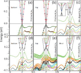
The DFT bandstructure of Mn dopants substituted on one (the TOP) of the slab surfaces
is plotted in Fig. 1(c), for the case .
It is characterized by the following features:
(i) the conical TSS belonging to the top surface (where the impurity resides) has been pushed up in energy.
The bottom TSS
is essentially unaffected by the impurity
[see also Figs. 1(d)-(e), where the bottom and top states are highlighted];
(ii) the two displaced conical TSSs exhibit avoided level crossings, with a gap of the order of meV,
at two symmetric -points with respect to ;
(iii) the Dirac point of the top (bottom) TSS is now
above (below) the Fermi energy (). For the top TSS there is an energy gap
of meV at the Dirac point [see the inset in Fig. 1(c)]. As we explain below, this
gap is caused by the TRS breaking due to magnetic doping.
For the bottom TSS the gap remains negligible, i.e. meV, as in the pristine case;
(iv) the states in the energy window ,
not belonging to the bottom TSS,
result from the complex hybridization of Mn –levels,
NN Se –levels
and the extended top TSS.
The meV gap at the Dirac point obtained in
our calculations matches reasonably well the meV
gap found experimentally for 1% Mn doping in Bi2Se3 Chen et al. (2010).
The energy gap is expected to increase for higher doping concentrations.
In order to explain some of these features,
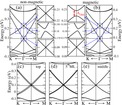
we employ the TB model for Bi2Se3, described in Section II.
Figures 2(a)-(b) show the bandstructure of 6QLs
of Bi2Se3 calculated with the TB model, where a non-magnetic or a magnetic impurity
is substituting Bi in the second ML below the surface.
In the non-magnetic case, as a result of asymmetric doping,
one of the two degenerate (for pristine Bi2Se3) conical TSSs,
corresponding to the doped surface,
is shifted up in energy. The TSS of the un-doped surface
remain nearly unaffected, as
expected for a relatively thick slab.
Since the TRS is preserved, the states at
have a two-fold degeneracy related to the opposite spins [top inset
in Fig. 2(a)]. However, the asymmetric doping
breaks the inversion symmetry (IS), therefore away from the degeneracy
is lifted and avoided crossings are formed at two symmetric -points,
producing a gap, which can be seen in the middle insets in Figs. 2(a) and (b)
(this gap should vanish in the limit of an infinitely thick slab).
The presence of the magnetization
breaks the TRS, which leads to the lifting of the
degeneracy at all –points. Indeed, in the magnetic case, in addition to the features related
to asymmetric doping, we find a gap at the Dirac point ()
for the TSS of the doped surface [top inset in Fig. 2(b)].
We focus specifically on three important regions in the
bandstructure, namely the Dirac point of the top surface
states [top inset in Fig. 2(b)], which interact with
impurity, the Dirac point of the bottom surface states
(unperturbed) [bottom inset in Fig. 2(b)], and
the avoided level crossings, which occur symmetrically on both
sides of the point and introduce a small gap
[middle inset in Fig. 2(b)]. The latter
feature, as well as the overall shape of the bandstructure consisting of two
shifted Dirac cones, is present in both non-magnetic and
magnetic cases. As we explain in detail below, it is caused
purely by IS breaking since the impurity is positioned on
only one of the surfaces of the slab.
However, the crucial difference between non-magnetic and
magnetic impurities is the opening of the gap at
the Dirac point of the TSS of the top surface, where the impurity is located.
This is a manifestation of the TRS breaking.
Note that the bottom TSS remain essentially unperturbed by the impurity in both cases.
We further investigate the effect of asymmetric doping by placing a non-magnetic impurity
at different positions in the slab [see Fig. 2(c)-(e)]. Note that in this case
the impurity substitutes Se and we use a 5QL slab; such configuration allows us to position
the impurity at the exact geometrical center of the slab, which is a Se monolayer (ML). We use a similar potential shift,
=, as in the
case of impurity substituting Bi. Placing the impurity close to one of the surfaces
shifts the corresponding Dirac cone
while the other one remains unchanged, provided that the slab is thick enough
so that the two surfaces do not interact strongly with each other [Fig. 2(c)].
As the impurity is moved further away from the surface, its interaction with the topological
surface states on the corresponding
surface decreases, reducing the shift of the Dirac-cone states [Fig. 2(d)].
Finally, when the impurity is placed in the middle of the slab, the IS is restored and
we find two degenerate Dirac cones with the position of the Dirac point coinciding with that
of the pristine slab.
Based on these calculations, we attribute similar features occurring
in the vicinity of the Fermi energy in the DFT bandstructure [See Fig. 1(c)]
to the IS breaking caused by asymmetric doping.
We now focus on the properties of the unoccupied electronic states,
appearing above the Fermi level in our DFT bandstructure
calculations [Figs. 1(c)-(f)]. There are three elements
contributing to these states, (i) the impurity levels
(Mn –orbitals), (ii) the Mn-acceptor states,
and (iii) the TSSs.
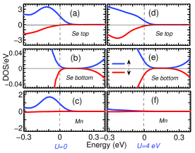
Figure 3 shows the
spin-resolved density of states (DOS) around the Fermi energy
for the –orbitals
of Se atoms on the top and bottom surfaces and
for the Mn –orbitals, for = and = eV.
The calculated magnetic moment of the Mn atom on the surface,
with spin orbit interaction (SOI), is 4.67 for = eV, indicating
that a substitutional Mn is close to its valence state.
Given the nominal valence state of Bi in Bi2Se3, we conclude
that the substitution of a Bi with a Mn introduces
an acceptor (hole) state. Its
wave function is localized primarily
on the surroundings of the dopant and, to a lesser degree, on the dopant itself.
For = some of the Mn –orbitals
appear close to the Fermi level [Fig. 3(c)],
in the same energy
range as the Se –orbitals,
leading to their hybridization.
Importantly, the top surface Se –states
around the Fermi level are visibly spin-polarized [Fig. 3(a)].
The -hybridized Se –orbitals above the Fermi level close to the Mn are
the main contributors to the Mn-acceptor (hole) states.
With increasing , the majority Mn –orbitals are pushed
deeper into the valence band [Fig. 3(f)],
decreasing the hybridization
with Se –orbitals on the top surface.
As a result, the Mn magnetic moment increases
by with respect to the value
and the spin-polarization of the top Se –states
decreases [Fig. 3(d)].
We find a similar dependence of the magnetic moment on electronic correlations
for Mn in the bulk, namely, 4.25
for = and 4.52 for = eV.
These results suggest that the discrepancy between recent DFT calculations,
reporting the values for the Mn
magnetic moment ranging from
4 Niu et al. (2011); Abdalla et al. (2013) to 4.58 Henk et al. (2012b, a)
for Bi2Se3 and Bi2Te3, might be originating
from different treatment of electron interactions
on the impurity site.
The appearance of these unoccupied states above the Fermi level,
spatially localized around the Mn,
is an indication of the acceptor level.
These states occur in the same energy range
eV
of the TSS of the top surface, and energetically are not far
from its Dirac point. This is crucial for the opening
of the gap.
In contrast, in the range eV, the bottom surface
states [Figs. 3(b) and (e)] are
essentially the TSS, with negligible coupling to the impurity wavefunction.
Their linear dispersion
is preserved and still detectable in
the bandstructure in Fig. 1(d).
To clarify the nature of the Mn-acceptor independently
of the TSS,
we perform calculations without SOI, which greatly simplifies
the electronic structure around the Fermi energy.
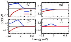
Figures 4(b)-(e) show the total DOS and
the partial DOS for the Mn impurity and surrounding Se atoms,
calculated without SOI.
We conclude that the peak in the total DOS (mainly majority spin)
right below the Fermi level, is predominantly due to the
Mn –levels and the NN Se
–levels, with a very small but finite contribution
from other Se atoms around the Mn [two Se atoms,
which are not NN to Mn, are indicated by arrows in Fig. 4(a)].
The highly spin-polarized character of the –states around
the Fermi level is a consequence of
the hybridization between the Mn orbitals and the NN Se orbitals.
Our calculations with = eV (not shown here) confirm
this observation. Similar to
the calculation with SOI (see Fig. 3),
for = eV the Mn -orbitals are more localized
and are pushed deeper into the valence band,
which reduces the – hybridization and decreases
the polarization of NN Se -states by a factor of two.
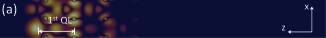
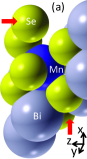
We now examine the spatial character of the Mn acceptor state,
which is directly accessible by STM experiments.
Figures 5(b)-(e) show simulated STM topographies
of Mn-doped Bi2Se3 in the vicinity of the (111)
surface. These images are obtained by plotting the
electronic local density of states (LDOS) around the Mn,
integrated in the energy
window eV (empty states) and eV (filled states)
around the Fermi level for =.
Figures 5(c) and (e) clearly show that the acceptor state is
predominately localized around the Mn and its three NN Se atoms.
The state is composed of three -like Se orbitals pointing to the Mn in the middle, visibly deformed by the hybridization.
It exhibits a characteristic triangular shape similar to the experimental STM topography observed at positive bias in
Mn-doped Bi2Te3 Hor et al. (2010).
The LDOS for filled states below the Fermi level [Figs. 5(b) and (d)] are much less affected
by the presence of the impurity.
The side view of the empty-state LDOS along the slab [Fig. 5(a)]
confirms that the states in the energy range eV are
predominantly localized around Mn and its NN Se atoms, which is a signature of the Mn-acceptor.
The figure also shows states that extend only within 1 QL from the surface, which is a typical
decay length of the TSS Pertsova and Canali (2014).
Clearly, the Mn-acceptor has a strong spatial overlap with the TSS of the top surface.
Furthermore, as shown above, these two states are quasi-degenerate in the energy range eV,
and therefore they couple strongly.
It is precisely the quasi-resonant coupling of the spin-chiral TSS with the spin-polarized Mn-acceptor
that ultimately opens a gap at the Dirac point. Strong support for this mechanism is provided by the observation that the gap decreases
from meV to meV when increases from 0 to 4 eV. Strong correlations at the impurity site decrease
the Mn – and Se –orbital hybridization, leading to a smaller spin-polarization of the acceptor.
Isolated spin-polarized Mn –levels
are further away both in energy and in space from the TSS at the Dirac point.
Therefore their spin-dependent potential alone is less effective in inducing the TRS breaking necessary to open a gap.
IV Conclusions
In conclusion, our calculations show, in agreement with
experiments Hor et al. (2010); Choi et al. (2013); Janíček et al. (2008), that
substitutional Mn impurities on Bi2Se3 surface
introduce spin-polarized acceptor states,
whose properties are similar to Mn-acceptors in GaAs.
The mechanism for
the opening of a gap at the Dirac point is provided by
the spatial overlap and the
quasi-resonant coupling between the Mn-acceptor
and the TSS
inside the bulk band gap of Bi2Se3.
The signatures of this coupling can be detected in STM experiments,
addressing specifically
magnetic dopants on a 3D TI surface.
The present study contributes to clarify the origin of surface-ferromagnetism
in transition-metal-doped Bi-chalcogenide thin films.
Finally, we should mention that recent infrared optical experiments in Mn-doped
Bi2Te3 thin films suggest that, despite the similarities to DMSs, carrier-independent
mechanisms such as super-exchange Niu et al. (2011) and the aforementioned enhanced Van Vleck spin
susceptibility Yu et al. (2010), might also be relevant for establishing
the ferromagnetic state Chapler et al. (2014). Specifically these experiments indicate that bulk charge
carriers control the optical response but do not seem to play a significant role in
mediating ferromagnetism. Note, however, that Mn-doped systems investigated in
Ref. Chapler et al., 2014 are always n-type rather than the expected p-type for substitutional Mn,
with the Fermi energy always located in the Bi2Te3 conduction band. The reason of this
fact is still unclear. In any case these systems are in a regime quite different from
the one studied in the present paper, where the position of Fermi energy is
characteristic of a p-type DMS.
Further experimental and theoretical
studies, addressing the role of bulk dopants and
the position of the Fermi level in the bulk band gap, are necessary to elucidate this point.
Acknowledgments
This work was supported by the Faculty of Technology at Linnaeus University, by the Swedish Research Council under Grant Number: 621-2010-3761, and the NordForsk research network 080134 “Nanospintronics: theory and simulations”. Computational resources have been provided by the Lunarc center for scientific and technical computing at Lund University.
References
- Hasan and Kane (2010) M. Z. Hasan and C. L. Kane, Rev. Mod. Phys. 82, 3045 (2010).
- Qi and Zhang (2011) X.-L. Qi and S.-C. Zhang, Rev. Mod. Phys. 83, 1057 (2011).
- Zhang et al. (2009) H. Zhang, C.-X. Liu, X.-L. Qi, X. Dai, Z. Fang, and S.-C. Zhang, Nature Physics 5, 438 (2009).
- Yu et al. (2010) R. Yu, W. Zhang, H.-J. Zhang, S.-C. Zhang, X. Dai, and Z. Fang, Science 329, 61 (2010).
- Chang et al. (2013) C.-Z. Chang, J. Zhang, X. Feng, J. Shen, Z. Zhang, M. Guo, K. Li, Y. Ou, P. Wei, L.-L. Wang, Z.-Q. Ji, Y. Feng, S. Ji, X. Chen, J. Jia, X. Dai, Z. Fang, S.-C. Zhang, K. He, Y. Wang, L. Lu, X.-C. Ma, and Q.-K. Xue, Science 340, 167 (2013).
- Qi et al. (2008) X.-L. Qi, T. L. Hughes, and S.-C. Zhang, Phys. Rev. B 78, 195424 (2008).
- Liu et al. (2009) Q. Liu, C.-X. Liu, C. Xu, X.-L. Qi, and S.-C. Zhang, Phys. Rev. Lett. 102, 156603 (2009).
- Checkelsky et al. (2012) J. G. Checkelsky, J. Ye, Y. Onose, and Y. Tokura, Nature Physics 8, 729 (2012).
- Niu et al. (2011) C. Niu, Y. Dai, M. Guo, W. Wei, Y. Ma, and B. Huang, Appl. Phys. Lett. 98, 252502 (2011).
- Henk et al. (2012a) J. Henk, M. Flieger, I. V. Maznichenko, I. Mertig, A. Ernst, S. V. Eremeev, and E. V. Chulkov, Phys. Rev. Lett. 109, 076801 (2012a).
- Abdalla et al. (2013) L. B. Abdalla, L. Seixas, T. M. Schmidt, R. H. Miwa, and A. Fazzio, Phys. Rev. B 88, 045312 (2013).
- Li et al. (2014) Y. Li, X. Zou, J. Li, and G. Zhou, The Journal of Chemical Physics 140, 124704 (2014).
- Chen et al. (2010) Y. L. Chen, J.-H. Chu, J. G. Analytis, Z. K. Liu, K. Igarashi, H.-H. Kuo, X. L. Qi, S. K. Mo, R. G. Moore, D. H. Lu, M. Hashimoto, T. Sasagawa, S. C. Zhang, I. R. Fisher, Z. Hussain, and Z. X. Shen, Science 329, 659 (2010).
- Scholz et al. (2012) M. R. Scholz, J. Sánchez-Barriga, D. Marchenko, A. Varykhalov, A. Volykhov, L. V. Yashina, and O. Rader, Phys. Rev. Lett. 108, 256810 (2012).
- Valla et al. (2012) T. Valla, Z.-H. Pan, D. Gardner, Y. S. Lee, and S. Chu, Phys. Rev. Lett. 108, 117601 (2012).
- Honolka et al. (2012) J. Honolka, A. A. Khajetoorians, V. Sessi, T. O. Wehling, S. Stepanow, J.-L. Mi, B. B. Iversen, T. Schlenk, J. Wiebe, N. B. Brookes, A. I. Lichtenstein, P. Hofmann, K. Kern, and R. Wiesendanger, Phys. Rev. Lett. 108, 256811 (2012).
- Schmidt et al. (2013) T. M. Schmidt, R. H. Miwa, and A. Fazzio, Journal of Physics: Condensed Matter 25, 445003 (2013).
- Wray et al. (2011) L. A. Wray, S.-Y. Xu, Y. Xia, D. Hsieh, A. V. Fedorov, Y. San Hor, R. J. Cava, A. Bansil, H. Lin, and M. Z. Hasan, Nature Physics 7, 32 (2011).
- Hor et al. (2010) Y. S. Hor, P. Roushan, H. Beidenkopf, J. Seo, D. Qu, J. G. Checkelsky, L. A. Wray, D. Hsieh, Y. Xia, S.-Y. Xu, D. Qian, M. Z. Hasan, N. P. Ong, A. Yazdani, and R. J. Cava, Phys. Rev. B 81, 195203 (2010).
- Xu et al. (2012) S.-Y. Xu, M. Neupane, C. Liu, D. Zhang, A. Richardella, L. A. Wray, N. Alidoust, M. Leandersson, T. Balasubramanian, J. Sánchez-Barriga, et al., Nature Physics 8, 616 (2012).
- Shelford et al. (2012) L. R. Shelford, T. Hesjedal, L. Collins-McIntyre, S. S. Dhesi, F. Maccherozzi, and G. van der Laan, Phys. Rev. B 86, 081304 (2012).
- Li et al. (2012) Z. L. Li, J. H. Yang, G. H. Chen, M.-H. Whangbo, H. J. Xiang, and X. G. Gong, Phys. Rev. B 85, 054426 (2012).
- Zhang et al. (2012) J.-M. Zhang, W. Zhu, Y. Zhang, D. Xiao, and Y. Yao, Phys. Rev. Lett. 109, 266405 (2012).
- Henk et al. (2012b) J. Henk, A. Ernst, S. V. Eremeev, E. V. Chulkov, I. V. Maznichenko, and I. Mertig, Phys. Rev. Lett. 108, 206801 (2012b).
- Schmidt et al. (2011) T. M. Schmidt, R. H. Miwa, and A. Fazzio, Phys. Rev. B 84, 245418 (2011).
- Biswas and Balatsky (2010) R. R. Biswas and A. V. Balatsky, Phys. Rev. B 81, 233405 (2010).
- Abanin and Pesin (2011) D. A. Abanin and D. A. Pesin, Phys. Rev. Lett. 106, 136802 (2011).
- Efimkin and Galitski (2014) D. K. Efimkin and V. Galitski, Phys. Rev. B 89, 115431 (2014).
- Choi et al. (2013) Y. H. Choi, N. H. Jo, K. J. Lee, H. W. Lee, Y. H. Jo, J. Kajino, T. Takabatake, K.-T. Ko, J.-H. Park, and M. H. Jung, Appl. Phys. Lett. 25, 206005 (2013).
- Janíček et al. (2008) P. Janíček, Č. Drašar, P. Lošták, J. Vejpravová, and V. Sechovskỳ, Physica B: Condensed Matter 403, 3553 (2008).
- Mahani et al. (2014) M. R. Mahani, M. F. Islam, A. Pertsova, and C. M. Canali, Phys. Rev. B 89, 165408 (2014).
- Anisimov et al. (1991) V. I. Anisimov, J. Zaanen, and O. K. Andersen, Phys. Rev. B 44, 943 (1991).
- Blaha et al. (2001) P. Blaha, K. Schwarz, G. K. H. Madsen, D. Kvasnicka, and J. Luitz, WIEN2k, An Augmented Plane Wave Plus Local Orbitals Program for Calculating Crystal properties (Vienna University of Technology, Austria) (2001).
- Perdew et al. (1996) J. P. Perdew, K. Burke, and M. Ernzerhof, Phys. Rev. Lett. 77, 3865 (1996).
- Kobayashi (2011) K. Kobayashi, Phys. Rev. B 84, 205424 (2011).
- Pertsova and Canali (2014) A. Pertsova and C. Canali, New J. Phys 16, 063022 (2014).
- Chapler et al. (2014) B. C. Chapler, K. W. Post, A. R. Richardella, J. S. Lee, J. Tao, N. Samarth, and D. N. Basov, Phys. Rev. B 89, 235308 (2014).