Electronic structure of spin frustrated magnets: Mn3O4 spinel and postspinel
Abstract
Mn3O4 is a spin frustrated magnet that adopts a tetragonally distorted spinel structure at ambient conditions and a CaMn2O4-type postspinel structure at high pressure. We conducted both optical measurements and ab initio calculations, and systematically studied the electronic band structures of both the spinel and postspinel Mn3O4 phases. For both phases, theoretical electronic structures are consistent with the optical absorption spectra, and display characteristic band-splitting of the conduction band. The band gap obtained from the absorption spectra is 1.91(6) eV for the spinel phase, and 0.94(2) eV for the postspinel phase. Both phases are charge-transfer type insulators. The Mn 3d g and O 2p form antibonding orbitals situated at the conduction band with higher energy.
pacs:
71., 75.47.Lx, 75.25.-jI Introduction
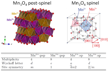
Manganese oxides have been exploited for a wide range of technological applications including electrode materials for batteries (MnO2) ammund00 , ultracapacitors for energy storage devices (MnO2) ammund00 , for the catalytic combustion of methane (Mn2O3) ramesh07 , and as electrochromic materials (Mn3O4) maru95 . Mn3O4 is a unique mixed-valence oxide that adopts a tetragonally distorted spinel structure (Figure 1) at ambient conditions amin26 ; xiao04 ; kimm11 ; bouch71 ; jensen74 ; char86 . This phase undergoes a structural phase transition at 15 GPa into a CaMn2O4-type phase, referred to as postspinel (Figure 1), which is quenchable to ambient pressure paris92 ; merlin10 ; hirai13 . Lattice, spin, and orbital degrees of freedom are strongly coupled in both phases hirai13 ; tack07 ; suzuki08 ; niiy13 ; kimm10 . Mn3O4 spinel undergoes three magnetic transitions ( K, K, K) jensen74 , exhibits pronounced magnetodielectric and magnetoelastic coupling tack07 ; suzuki08 ; niiy13 , and a quantum phase transition kimm11 ; kimm10 . It adopts three magnetic structures, (i) : a so-called Yafet-Kittel magnetic structure yafet52 in which Mn2+ and Mn3+ spins lie on the (1 -1 0) plane in a triangular spin configuration (Yafet-Kittel phase) bouch71 ; jensen74 ; char86 , (ii) : a conical jensen74 or sinusoidal char86 magnetic structure incommensurate with the chemical unit cell, and (iii) : a commensurate magnetic structure with the magnetic unit cell of the Yafet-Kittel phase doubled along the [1 1 0] direction. This complicated magnetic structure implies that Mn3O4 spinel is a spin frustrated magnet tack07 ; suzuki08 ; niiy13 ; kimm10 ; kuriki03 ; chung13 . Mn3O4 postspinel undergoes a giant atomic displacement near its = 210 K due to the coupled effect of the metastable structure with the orbital realignment of the Mn3+ ion hirai13 . Below 210 K, the postspinel phase of Mn3O4 adopts a magnetic structure in which Mn3+ spins align antiferromagnetically along the edge-sharing a axis, with a magnetic propagation vector k =[1/2,0,0] hirai13 . In contrast, Mn2+ spins are geometrically frustrated since they are situated at the center of a honeycomb arrangement of Mn3+ spins that are antiferromagnetically ordered, and exhibit a short-range magnetic order only below 55 K hirai13 .
Therefore, both of these phases are magnetically frustrated hirai13 ; tack07 ; suzuki08 ; niiy13 ; kimm10 ; kuriki03 ; chung13 , providing an important playground for systematically studying the electronic band structures of spin frustrated magnets nisoli13 . Electrical resistivity for the bulk polycrystalline samples are cm rozh66 for the spinel phase, and cm hirai13 for the postspinel phase. Previous studies on the band structure of Mn3O4 spinel are limited to theoretical studies using Hartree-Fock chart99 and density functional theory (DFT) calculations franch07 , which have significant disagreement in their results. While there are a few studies reported for thin film ( eV) dubal10 and nanoparticles ( eV) jhaa12 for Mn3O4 spinel, no optical studies have been reported for bulk polycrystalline and single crystalline samples of Mn3O4 spinel or postspinel.
In this study, we found that both phases of Mn3O4 possess characteristic band-splitting of the conduction band. Theoretical electronic structures are consistent with absorption spectra, where the band gap is 1.91(6) eV for the spinel phase and 0.94(2) eV for the postspinel phase. Both phases are charge-transfer type insulators. Mn 3d g and O 2p form antibonding orbitals situated at the conduction band with higher energy.
II Experiments
Polycrystalline samples of Mn3O4 spinel and postspinel were prepared at ambient and high pressure, respectively hirai13 . The spinel phase was prepared by heating MnCO3 (Alfa Aesar, 99.99 %) in air at 1400 K for 16 h. The postspinel phase was prepared by pressurizing the spinel phase up to 20 GPa using a cell fitted with polycrystalline diamond double toroidal anvils, followed by slow decompression to ambient pressure. Purity of the samples was examined by using synchrotron X-ray diffraction (XRD) ( nm) at beamline 16-BMD of the advanced photon source (APS), Argonne National Laboratory (ANL) hirai13 .
Total diffuse reflectance spectra of Mn3O4 spinel and postspinel were measured using a spectrometer equipped with an integrating sphere (Hitachi High-Tech, U-4100). Al2O3 powder was used as a standard reference. Then, the diffuse reflectance spectra were converted to absorption spectra using the Kubelka-Munk equation, (1-R)2/2R = /s, where R, and s denote reflectivity, absorption coefficient and scattering factor, respectively kubelk31 . The optical band gap was deduced from the linear extrapolation of absorption spectra with energy.
Ab initio calculations were performed using the plane-wave projector augmented-wave (PAW) method blochl94 ; kresse99 implemented in Vienna Ab initio Simulation Package (VASP) code kresse96 ; kress96 . Three different approximations to treat exchange-correlation potential were applied: (i) the generalized gradient approximation (GGA) by the Perdew-Becke-Ernzerhof (PBE) method perdew96 , (ii) the PBE plus a on-site Coulomb repulsion (U) term following the approach of Dudarev dudar98 for effective value of the Coulomb parameter ( = U-J, where J being an intra-atomic exchange parameter), and (iii) the hybrid functionals by the Heyd, Scuseria, and Ernzerhof (HSE06) method heyd03 , where correlation is described in GGA (PBE) and its exchange is a mixture of 25 % exact Hartree-Fock and 75 % PBE exchange. We used the lattice constants of a = 0.5756 nm and c = 0.9439 nm at 4.2 K bouch71 for the spinel phase and a = 0.3020 nm, b = 0.9842 nm, and c = 0.9568 nm at 60 K hirai13 for the postspinel phase, which were determined by neutron diffraction. We used the lattice constants at 60 K for the postspinel phase since the atomic coordinates could not be determined from neutron diffraction due to the contribution of short-range ordered Mn2+ spins hirai13 . Also a 2 supercell was constructed to investigate the magnetic structure of postspinel. The Brillouin zone was sampled by a 3 and a 3 Monkhorst-Pack grid monkh76 for the spinel and postspinel phases, respectively. A cutoff of 450 eV was chosen for the plane-wave basis set for both phases. Hellmann-Feynman forces were reduced until 0.5 eV nm-1 for the spinel phase, while the atomic coordinates for the postspinel phase were fixed at the initial input value due to its metastable nature hirai13 .
III Results and discussion
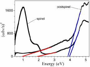
Figure 2 shows the absorption spectra of Mn3O4 spinel and postspinel, converted from diffuse reflectance spectra using the Kubelka-Munk equation kubelk31 . Red and blue lines are guide for estimating the optical band gap of the two energy levels of the conduction band in these phases. Ab initio calculations were also performed in order to obtain the theoretical band gap. Table 1 shows the experimental band gap from optical absorption spectra and the theoretical band gap from ab initio calculations for Mn3O4 spinel and postspinel. Both methods show a consistent band structure with characteristic band-splitting of the conduction band (Table 1 and Figure 3). The band gap obtained from optical absorption spectra is 1.91(6) eV for the spinel phase and 0.94(2) eV for the postspinel phase. The calculated band structure will be presented for both phases, and then their electronic structures will be further discussed.
| Methods | :sp (eV) | :sp (eV) | :psp (eV) | :psp (eV) |
|---|---|---|---|---|
| U-J=4 eV | 1.36 | 3.17 | 0.36 | 2.81 |
| U-J=5 eV | 1.46 | 3.47 | 0.55 | 3.40 |
| U-J=6 eV | 1.48 | 3.60 | 0.56 | 3.71 |
| HSE06 | 2.61 | 4.17 | 1.34 | 3.56 |
| Experimental | 1.91(6) | 3.96(9) | 0.94(2) | 3.86(6) |
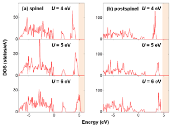
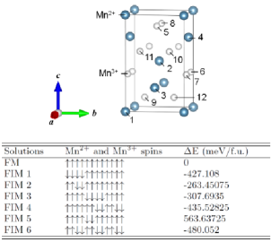
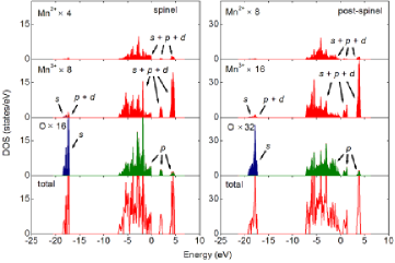
First, the band structure of Mn3O4 spinel will be discussed. Figure 3(a) shows the DOS calculated for Mn3O4 spinel with U-J = 4, 5, 6 eV. HSE06 calculations (Figure 4(a)) was conducted as well as PBE+U calculations, and all these calculations give a widely spread valence band and a characteristic band-splitting of the conduction band (Figure 3(a) and Figure 4(a)). This band-splitting of the conduction band is allowed since the work function of manganese oxides (e.g. MnO) is in a range of 4.6-6.6 eV toroker11 . The band gap and the energetically most stable magnetic structure (Figure 5, referred to as FIM 6 in a previous study chart99 ) of Mn3O4 spinel obtained from the ab initio calculations is consistent with Chartier et al chart99 and the previously reported cell-doubled magnetic structure below 33 K obtained from neutron diffraction studies bouch71 ; jensen74 ; char86 .
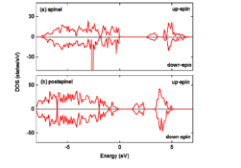
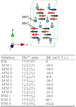
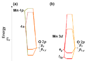
Next, the band structure of Mn3O4 postspinel will be discussed. The band gap of the postspinel phase (0.94(2) eV from optical absorption spectra) is about 1 eV smaller than that of the spinel phase (Table 1). Figure 3(b) and Figure 4(b) show the DOS calculated for Mn3O4 postspinel, where all the calculations give a wide valence band and characteristic band-splitting of the conduction band, similar to what was observed for the spinel phase. The two most stable magnetic structure calculated by this study (AFM 3 and AFM 7 in Figure 6) does not contradict with the short-range magnetic order of Mn2+ spins below 55 K since the canted Mn2+ spins allow ferromagnetic net magnetization hirai13 . The energy difference between AFM 3 and AFM 7 (Figure 6) is only 3.1 meV/f.u., which is comparable with the thermal fluctuation of meV at 55 K. Therefore, ab initio calculation demonstrates that Mn3O4 postspinel is a spin frustrated magnet and the small energy difference between two AFM solutions is in harmony with the experimentally observed short-range magnetic order below 55 K hirai13 . Since the calculated band gap is in good agreement with the optical absorption spectra and the most stable magnetic structure does not contradict with the neutron diffraction studies for both phases bouch71 ; jensen74 ; char86 ; hirai13 , the electronic band structure of Mn3O4 is further explored on the basis of ab initio calculation. Hereafter we will employ the up-spin DOS with U-J = 5 eV for the phases, since the selection of U-J parameter does not change its DOS structure to a great extent. Figure 7 demonstrates that Mn 3d orbitals are widely spread over the valence band, and they have significant overlap with the O 2p orbitals. Although the band width becomes narrower, this feature is maintained for the conduction band as well.
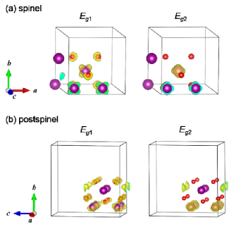
Mn3O4 spinel has a tetragonal symmetry (space group: I41/amd(141)), which results in the Mn 3d orbitals being split into three nondegenerate levels and a doubly degenerate level. Figure 8(a) shows the theoretical local charge density map of Mn3+O6 octahedra calculated for the two energy levels of the conduction band in Mn3O4 spinel. Since the theoretical DOS of Mn2+ electrons in the conduction band is very small, the theoretical DOS of Mn3+ electrons sufficiently represent the total DOS for Mn 3d electrons in the conduction band. The multiplicity, Wyckoff letter, and site symmetry for Mn3+ in Mn3O4 spinel are 8, d, and 2/m, respectively. Provided that the Mn 3d orbitals pointing toward the O atom are g and the rest are , the projection of charge distribution for Mn 3a electrons (Figure 8(a)) suggests that the conduction band with lower energy () corresponds to Mn 3d g, and the conduction band with higher energy () corresponds to Mn 3d (Figure 9).
Mn3O4 postspinel has an orthorhombic symmetry (space group: Pbcm(57)), which results in the Mn 3d levels being five nondegenerate levels. The multiplicity, Wyckoff letter, and site symmetry of Mn3+ in Mn3O4 postspinel are 8, e, and 1, respectively. Analogous to the spinel phase, the projection of charge distribution for Mn 3d electrons of Mn3O4 postspinel (Figure 8(b)) suggests that the conduction band with lower energy () corresponds to Mn 3d g, and the conduction band with higher energy () corresponds to Mn 3d (Figure 9). Therefore, for both phases, Mn 3d orbitals overlap with O 2p orbitals in the valence band at the lower energy level of g and . In other words, the Mn 3d levels split into bonding and antibonding levels forming hybridized orbitals with ligand O 2p orbitals. Both phases of Mn3O4 are charge-transfer type insulators with characteristic band-splitting of the conduction band (Figure 3 and Figure 7).
IV Conclusion
Electronic structures of Mn3O4 spinel and postspinel were systematically studied. Ab initio calculations and the optical measurements were performed on both phases, resulting in a consistent band structure with characteristic band-splitting of the conduction band. We obtained the band gap of 1.91(6) eV for the spinel phase, and 0.94(2) eV for the postspinel phase. Both phases of Mn3O4 are charge-transfer type insulators, and Mn 3d g and O 2p form antibonding orbitals situated at the conduction band with higher energy. Ab initio calculations also demonstrate that Mn3O4 postspinel is a spin frustrated magnet.
V Acknowledgements
This research is funded by the U.S. Department of Energy (DOE), Office of Basic Energy Sciences (BES). S.H. and W.L.M. are supported by the U.S. Department of Energy (DOE), Office of Basic Energy Sciences (BES), Division of Materials Sciences and Engineering, under Contact No. DE-AC02-76SF00515.
References
- (1) B. Ammundsen, J. Desilvestro, T. Groutso, D. Hassell, J. Metson, E. Regan, R. Steiner, and P. Pickering, J. Electrochem. Soc. 147, 4078 (2000).
- (2) K. Ramesh, L. Chen, F. Chen, Z. Zhong, J. Chin, H. Mook, and Y. Han, Catal. Commun. 8, 1421 (2007).
- (3) T. Maruyama and Y. Osaki, J. Electrochem. Soc. 142, 3137 (1995).
- (4) G. Aminoff, Z. Kristallogr. 64, 475 (1926).
- (5) Y. Xiao, D. E. Wittmer, F. Izumi, S. Mini, T. Graber, and P. J. Viccaro, Appl. Phys. Lett. 85, 736 (2004).
- (6) M. Kim, X. M. Chen, X. Wang, C. S. Nelson, R. Budakian, P. Abbamonte, and S. L. Cooper, Phys. Rev. B 84, 174424 (2011).
- (7) B. Boucher, R. Buhl, and M. Perrin, J. Phys. Chem. Solids 32, 2429 (1971).
- (8) G. B. Jensen and O. V. Nielsen, J. Phys. C 7, 409 (1974).
- (9) B. Chardon and F. Vigneron, J. Mag. Mag. Mat. 58, 128 (1986).
- (10) E. Paris, C. R. II Ross, and H. Olijnyk, Eur. J. Mineral. 4, 87 (1992).
- (11) M. Merlini, M. Hanfland, M. Gemmi, S. Huotari, L. Simonelli, P. Strobel, Am. Mineral. 95, 200 (2010).
- (12) S. Hirai, A.M. dos Santos, M.C. Shapiro, J.J. Molaison, N. Pradhan, M. Guthrie, C.A. Tulk, I.R. Fisher, and W.L. Mao, Phys. Rev. B 87, 014417 (2013).
- (13) R. Tackett, G. Lawes, B.C. Melot, M. Grossman, E.S. Toberer and R. Seshadri, Phys. Rev. B 76, 024409 (2007).
- (14) T. Suzuki and T. Katsufuji, Phys. Rev. B 77, 220402 (2008).
- (15) Y. Nii, H. Sagayama, H. Umetsu, N. Abe, K. Taniguchi, and T. Arima, Phys. Rev. B 87, 195115 (2013).
- (16) M. Kim, X. M. Chen, Y. I. Joe, E. Fradkin, P. Abbamonte, and S. L. Cooper, Phys. Rev. Lett. 104, 136402 (2010).
- (17) Y. Yafet and C. Kittel, Phys. Rev. 87, 290 (1952).
- (18) A. Kuriki, Y. Moritomo, S. Xu, K. Ohoyama, K. Kato, and A. Nakamura, J. Phys. Soc. Jpn. 72, 458 (2003)
- (19) J. –H. Chung, K. H. Lee, Y. –S. Song, T. Suzuki, and T. Katsufuji, J. Phys. Soc. Jpn. 82, 034707 (2013).
- (20) C. Nisoli, R. Moessner, and P. Schiffer, Rev. Mod. Phys. 85, 1473 (2013).
- (21) M. V. Rozhdestvenskaya, V. A. Mokievskii, and V. A. Stogova, Kristallografiya 11, 903 (1966).
- (22) A. Chartier, P. D’Arco, R. Dovesi, and V.R. Saunders, Phys. Rev. B 60, 14042 (1999).
- (23) C. Franchini, R. Podloucky, J. Paier, M. Marsman, and G. Kresse, Phys. Rev. B 75, 195128 (2007).
- (24) D.P. Dubal, D.S. Dhawale, R.R. Salunkhe, V.J. Fulari, and C.D. Lokhande, J. Alloys Compd. 497, 166 (2010).
- (25) A. Jha, R. Thapa, and K.K. Chattopadhyay, Mater. Res. Bull. 47, 813 (2012).
- (26) P. Kubelka and F. Munk, Z. Tech. Phys. (Leipzig) 12, 593 (1931).
- (27) P. E. Blochl, Phys. Rev. B 50, 17953 (1994).
- (28) G. Kresse and D. Joubert, Phys. Rev. B 59, 1758 (1999).
- (29) G. Kresse and J. Furthmiiller, Comput. Mater. Sci. 6, 15 (1996).
- (30) G. Kresse and J. Furthmüller, Phys. Rev. B 54, 11169 (1996).
- (31) J. P. Perdew, K. Burke, and M. Emzerhof, Phys. Rev. Lett. 77, 3865 (1996).
- (32) S. L. Dudarev, G. A. Botton, S. Y. Savrasov, C. J. Humphreys, and A. P. Sutton, Phys. Rev. B 57, 1505 (1998).
- (33) J. Heyd, G. E. Scuseria, and M. Ernzerhof, J. Chem. Phys. 118, 8207 (2003).
- (34) H. J. Monkhorst and J. D. Pack, Phys. Rev. B 13, 5188 (1976).
- (35) M. C. Toroker, D. K. Kanan, N. Alidoust, L. Y. Isseroff, P. Liao, and E. A. Carter, Phys. Chem. Chem. Phys. 13, 16644 (2011).