Magnetic field resistant quantum interferences in bismuth nanowires based Josephson junctions
Abstract
We investigate proximity induced superconductivity in micrometer-long bismuth nanowires connected to superconducting electrodes with a high critical field. At low temperature we measure a supercurrent that persists in magnetic fields as high as the critical field of the electrodes (above 11 T). The critical current is also strongly modulated by the magnetic field. In certain samples we find regular, rapid SQUID-like periodic oscillations occurring up to high fields. Other samples exhibit less periodic but full modulations of the critical current on Tesla field scales, with field-caused extinctions of the supercurrent. These findings indicate the existence of low dimensionally, phase coherent, interfering conducting regions through the samples, with a subtle interplay between orbital and spin contributions. We relate these surprising results to the electronic properties of the surface states of bismuth, strong Rashba spin-orbit coupling, large effective g factors, and their effect on the induced superconducting correlations.
73.63.-b, 74.45.+c, 74.78.-w, 74.78.Na
In the superconducting proximity effect, singlet pair correlations can penetrate quite far (on the micron scale) into a non superconducting (normal) conductor. This penetration, that can lead to supercurrents through normal conductors several micrometers long connected to two superconductors, results from quantum interference between all conduction channels in the sample. In a microscopic picture, the supercurrent is carried by Andreev states, combinations of time reversed electron and hole wavefunctions confined to the normal conductor. It is thus natural to consider that this interference is destroyed not only by inelastic scattering, but also by time reversal symmetry breaking. Indeed, a magnetic field is known to suppress the supercurrent via both orbital (Aharonov Bohm phase accumulation) and spin (Zeeman dephasing) effects. Nevertheless, supercurrents have been induced through ferromagnets. The oscillatory sign and decaying intensity of the supercurrent with increasing ferromagnet thickness is an illustration of the dephasing role played by the exchange field. On the other hand, the time reversal invariant spin orbit interactions, by imposing strong correlations between spatial and spin components of the induced Andreev pairs, offer new possibilities such as coupling between singlet and triplet pairing gorkov ; bergeret , arbitrary Josephson phase shifts in an exchange or a Zeeman field ( junction behavior) buzdin ; feinberg ; nazarov and the possible formation of Majorana fermions at the interface between semiconducting nanowires and superconducting electrodes frolov .
In this Letter, we probe the superconducting proximity effect in crystalline bismuth nanowires, a system with extremely high Rashba spin orbit coupling (SOC), connected to superconducting electrodes with standard s-wave pairing and a very high critical field . The complex interference pattern we measure, up to magnetic fields such that the Zeeman energy, , becomes of the order of the spin-orbit and Fermi energies (), uniquely reveals the role played by both spin and orbital degrees of freedom.
Bismuth is a semi-metal with rhombohedral structure whose bulk electronic properties have been extensively studied: three barely filled electron bands coexist with a single, nearly filled, heavy hole band. Bi’s strong atomic spin orbit energy leads to extremely high effective g factors (), that depend on the applied magnetic field direction. Moreover the semi-metallic character leads to unusually large Fermi wavelengths, hofman . Therefore in nanostructures only a few thick or wide, because of quantum confinement, the surface states rather than the bulk states should play a major role, in particular in the transport properties nikolaeva ; ning . Angle-resolved photoemission (ARPES) revealed electronic surface states in Bi with almost free electronic mass and nanometer-size . These states are remarkable in that the energy bands display a huge Rashba spin splitting, because of the loss of inversion symmetry at the surface combined with Bi’s high atomic SOC. ARPES of differently oriented Bi surfaces hofmanarpes and spin resolved ARPES Hirahara have found spin splitting energies of about 0.1 eV, as high as . The (111) surface, perpendicular to the rhombohedral axis, is particular because it possesses states on the top bilayer, that are decoupled from the bulk states. One dimensional quantum spin Hall states have even been predicted at the edge of these (111) surfaces murakami . Quite recently, scanning tunneling microscopy have indeed found 1D edge states around single crystalline bilayer islands on the top of BiSe or bulk Bi(111) crystals STM ; Yazdani . 1D topological states of (114) surfaces have also been seen by ARPES Bi114 . Thus 100 nm-wide Bi nanowires seem ideal to investigate the effect of SOC on the superconducting proximity effect, in a regime barely explored up to now, in which the spin-splitting energy of carriers is comparable to . In addition, the surface states ’ relatively high (between 10 and 100, depending on the surface orientation with respect to the magnetic field) Seradjeh , imply that can also reach and spin splitting energy at fields on the 10 T scale. Finally, the relative directions between the Zeeman and orbital fields can be varied, leading to even richer physics.
In the following, we present experiments on Bi nanowires connected to high superconducting electrodes that show striking differences with ordinary Josephson SNS junctions: the supercurrent persists up to magnetic fields as high as the of the electrodes (11 T). In some cases the field even enhances the critical current . In addition, we find oscillations of : some samples display both a periodic squid-like oscillation with a period in the hundred Gauss range and a higher, Tesla range, modulation, while in other samples only a strong high field modulation is found, with the complete extinction of at specific fields. These findings point to the existence of interfering Andreev pairs confined to a small number of conducting regions of low dimensionality. A subtle interplay between orbital and spin contributions is also required to explain the extent and period of interference. We discuss these unusual results in view of the properties of Bi’s surface states, the very strong Rashba SOC, and high anisotropic .
The Bi nanowires are electrochemically grown in the -wide pores of a polycarbonate track-etched membrane, and released by dissolution of the membrane (supplementary materials). X-ray diffraction and transmission electron microscopy demonstrate the high crystallinity of the few--long nanowires, with no high angle grain boundaries. An approximately 10 to 20 nm-thick external amorphous layer is also found, probably a protective residual polycarbonate coating. Given the nm-size of Bi’s surface states hofman , more than 100 conduction channels are expected at the surface of the wires. The nanowires are most likely faceted polyhedra, with each facet having a potentially different crystalline orientation. Thus some facets can be insulating murakamiPRB while others, such as (111) or (114) facets, may have very specific conduction properties. The nanowires are deposited onto an oxidized Si substrate with prepatterned electrodes. The superconducting contacts to the Bi nanowires, and connection to the electrodes, are realized in a dual electron and ion beam microscope equipped with a gas injection system: the focused Ga ion beam (FIB) decomposes a tungsten carbonyl vapor, producing a carbon and gallium-doped amorphous tungsten wire roughly 100 nm thick and wide. The superconductive properties of these wires are impressive, with a transition temperature , , and above 11 T at low temperature (LT) kasumov05 . The superconducting gap measured by scanning tunneling spectroscopy viera is meV. We have checked that SNS junctions with -long Au wires contacted in this way behave similarly to more conventionally fabricated SNS junctions chiodi . Because the FIB can be used to etch the Bi wire and coating at the contact before W deposition, this technique ensures a good, albeit not perfect, transparency. The contacts degrade with time, so the samples were cooled within hours of their connection, except for one sample (Bi3, see below) that was kept several weeks in vacuum at 300K after the first set of measurements, and whose resistance doubled.
We have investigated the LT resistance of ten such samples. Below the of the W electrodes, the resistance is mostly due to the two probe resistance of the Bi nanowires. Although the wires have similar dimensions, this resistance varies widely, between 1 and 30 k. Since the intrinsic resistance of the Bi wires is only expected to be few hundred (if one extrapolates reports on much longer wires of similar diameters nikolaeva ), this indicates that the wire/contact interface resistance dominates.
Proximity induced superconductivity gives rise to a resistance decrease below the of the W electrodes in five samples out of ten. A supercurrent, corresponding to a zero resistance state, is detectable in three samples. Two other samples display an incomplete proximity effect: the resistance drop is small (3 to 10 percent), and turns into a resistance increase (of about 10 percent) as the temperature is lowered further. The LT differential resistance of those two samples is peaked at low current, due to the interplay of interactions and a low transparency of the Bi/W interface morpurgo . These results are an indication that our Bi nanowires are not intrinsically superconducting, in contrast to the superconductivity below 1 K found in prior work on Bi nanowires chan . Those nanowires were unprotected against oxidation, resulting in more pronounced surface disorder than ours. Kobayashi et al. also found intrinsic superconductivity with and in highly disordered nanowires with nm-size grains, but no intrinsic superconductivity down to 0.5 K in oxide-free cristalline Bi nanowires kobayashi . There is however one report of intrinsic superconductivity in arrays of single crystal Bi nanowires grown, as ours, in polycarbonate membranes (but with a different electrolyte) ye08 , with and smaller than 0.5 T.

In the following we focus on the 3 samples with a detectable supercurrent, , and , all of which are 2 long. Their normal state resistances , measured below the W wires’ , are respectively 1, 13 and . We also present successive cool downs of , with changed orientations between wire and field. The sample is called since its room temperature resistance increased to , implying a worsening of the contact to the W electrodes. The zero bias resistance drops to zero below 0.8 K, and the differential resistance curves display a zero resistance state for currents below a switching current of , and for , and respectively, in zero magnetic field and at 100 mK. In the following, we equate this switching current and . We also extrapolate for even though it does not display a fully zero resistance state. The product ranges between 0.75 and 1.5 meV, the same order of magnitude as the superconducting gap of the W wires. This is consistent with what is expected of short Josephson SNS junctions with an induced gap of the order of the gap of the electrodes. The short junction behavior implies that the superconducting gap is less than 10 times the Thouless energy dubos . A Fermi velocity m/s yields a mean free path , which confirms the ballistic nature of transport through the wires. The temperature dependence of ’s differential resistance, and the Shapiro steps under irradiation at frequency f, that appear at the expected dc voltages , are shown in supplementary materials.
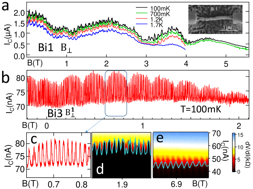
Our most striking result concerns the magnetic field dependence of (see Figs. 1 and 2, with the field perpendicular to the wires, and Fig. 3 with 3 different orientations). First, we find that the supercurrent persists up to very high fields: higher than 6 T for and , and 11 T for : in all cases those values are merely limited by the highest field achievable with the superconducting magnets used in the experiments. Second, of all three samples is strongly modulated by the magnetic field: two samples, and , display SQUID-like oscillations of , with a period of 800 G for and 140 G for . These rapid oscillations persist to high fields, up to 10 T for (not shown).
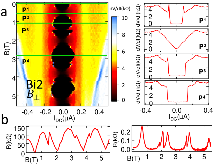
The critical current of is also modulated with a second period of about 0.3 T. Finally, is also modulated aperiodically on the Tesla scale for , and (see Figs. 1, 2 and 3). In samples without rapid SQUID-like oscillations, the high field modulation causes a full extinction of the supercurrent in and , with entire magnetic field intervals having zero supercurrent and finite resistance. We also explored 3 perpendicular field orientations for , including one along the wire axis (Fig. 3). The field modulation patterns of differ. High resistance peaks occur at different fields (8, 9 and 5 T, see Fig. 3). The small-period, squid-like oscillations of the first cool-down are not detectable in these subsequent cool downs.
We now discuss these complex interference patterns by considering field-induced phase shifts of the Andreev pairs wave functions, whose origin, involve either orbital or spin degrees of freedom. We first recall the generic field dependence of of ordinary SNS junctions, with a very high number of conduction channels. is strongly suppressed by magnetic field due to two different pair breaking mechanisms. In the semi-classical limit ( much smaller than all sample dimensions), orbital phase breaking is due to the Aharonov Bohm phase difference between different Andreev pairs that follow different trajectories through the N. This orbital dephasing suppresses the supercurrent at fields corresponding to a flux quantum through the sample, as observed experimentally e.g. in Au wires chiodi . In samples with a very small area perpendicular to the magnetic field, this orbital dephasing is weak, and the spin phase breaking caused by the Zeeman effect becomes noticeable. The Zeeman effect causes a phase difference between the electron and hole components of a given Andreev pair, given by on a trajectory of length ( is the time to cross the sample). Summing the contributions of all Andreev pairs trajectories, when the number of channels is large, yields an exponential supercurrent suppression with magnetic field.
All three Bi wires have an area perpendicular to the magnetic field of by , so that one flux quantum corresponds to a magnetic field of 50 G, three orders of magnitude smaller than the supercurrent extinction field found in the experiment. The persistence of supercurrents to fields as high as 10 T can only be understood if transport is confined to very few, quasi ballistic, 1D channels whose width should not exceed . These channels could be located along the edges of particular facets parallel to the nanowire axis cylinder . The small period (few 100 G), SQUID-like oscillations of in and , are then the manifestation of quantum interference between Andreev pairs belonging to two such 1D edge channels. Such topological edge states could be those of the (111) or (114) surfaces, or of others possessing similar topological properties. Since the period of the oscillation corresponds to the flux enclosed between the interfering channels, the measured periods of 140 G for and 800 G for would correspond to 1D channels along the samples axis, distant by 70 and 12 nm respectively. This interference pattern, that we interpret as due to the concentration of current along certain edges, recalls the recent observation of periodic oscillations of the Josephson current carried by spin Hall edge states in a 2D topological insulator connected to superconducting electrodes Yacoby .
We now discuss the supercurrent modulations at higher field, and argue that they are due to the difference between the electron and hole wavevectors of the Andreev pairs. The magnetic field, via , shifts the wavevectors of carriers of opposite spin at the Fermi level feinberg ; nazarov . Within linear approximation, the phase difference accumulated between the electron and hole components of opposite spin along a 1D ballistic trajectory of length is ioselevitch ; buzdin , with the field component along the spin orbit field. (Note the exact similarity to 1D ballistic superconducting/ferromagnetic/superconducting (SFS) junctions, buzdinRMP ). Typical Bi surface states parameters (3 and ) yield a characteristic modulation period in the Tesla range, so that we believe that the large field modulations of seen on all the samples are due to this spin dephasing effect. The difference in actual interference pattern of the various samples, as well as for the three field orientations of , is expected, given the anisotropy of the Bi facets and the corresponding different , that can vary by more than an order of magnitude. It is easy to reproduce the experimental data on by considering the interference between two channels of transmissions differing by a factor 8, enclosing a surface of the order of the sample area. One has to take for the weakly transmitting channel, yielding an amplitude modulation of the small-period orbital SQUID-like oscillations with a 0.3 T period, and a much smaller for the strongly transmitting channel mironov .
In this picture, the full extinction of the supercurrent at nearly periodic field values is attributed to the Zeeman-induced phase differences (with integer) between the electron and hole components of the supercurrent-carrying Andreev pairs. Such full extinction (complete destructive interference) is thus restricted to a single current-carrying channel. This seems to be the case in and , since they do not display SQUID-like oscillations (that require two channels). The behavior is especially dramatic around 5 T (Fig. 3 c and c’), with a zero bias resistance that peaks at a value even higher than the normal state resistance. A final important finding is the enhancement of by the magnetic-field. ’s critical current at 5 T is twice that of zero field (Fig. 2a and b). A similar but smaller increase between 0 and 0.75 T is also seen in (Fig. 1b). This increase of with field may be attributable to the strong SOC, as predicted in junctions buzdin ; mironov .
We have shown evidence of quantum interference in Bi nanowires-based Josephson junctions, that persist up to very high magnetic fields. Sample dependent periodic oscillations of the critical current reveal complex interference patterns involving both orbital and spin degrees of freedom between a small number of strongly confined 1D channels, possibly located at the edges between facets of different crystalline orientations along the wires. The physical origin of this confinement of induced superconductivity in such quasi one-dimensional channels is not yet well understood. One possibility is that the confinement is favored in the superconducting state by the high magnetic field, that is known to induce inhomogeneous superconductivity in 2D superconductors with large Rashba SOC Barzykin .
We acknowledge fruitful discussions with Alexei Chepelianskii, Michael Feigelman, Pavel Ioselevich, Pascal Simon, Sacha Buzdin and Sergey Mironov. This work is supported by a Franco-Russian RFBR grant 13-02-91058-CNRS. The LPS group benefits from financial support from CNRS and of the French national research agency (ANR SUPERGRAPH and MASH).
References
- (1) Lev P. Gor’kov and Emmanuel I. Rashba, Phys. Rev. Lett. 87, 037004 (2001).
- (2) F. S. Bergeret, A. F. Volkov, K. B. Efetov Rev. Mod. Phys. 77, 1321 (2005).
- (3) A.Buzdin, Phys. Rev. Lett. 101, 107005 (2008).
- (4) R. M. Lutchyn, J. D. Sau, and S. D. Sarma, Phys. Rev. Lett. 105, 077001 (2010). V. Mourik , K. Zuo, S. M. Frolov, S. R. Plissard, E. P. A. M. Bakk and L. P. Kouwenhoven, Science 336 1003 (2012).
- (5) A. A. Reynoso G. Usaj, C. A. Balseiro, D. Feinberg, and M. Avignon, Phys. Rev. B 86, 214519 (2012).
- (6) Tomohiro Yokoyama, Mikio Eto, Yuli V. Nazarov Phys. Rev. B 89, 195407 (2014.)
- (7) P. Hoffman, Progress in Surface Science 81 191245 (2006).
- (8) A. Nikolaeva , D. Gitsu, L. Konopko, M. J. Graf, and T. E. Huber Phys. Rev. B 77, 075332 (2008).
- (9) Wei Ning et al. arXiv:1404.5702
- (10) Yu. M. Koroteev G. Bihlmayer, J. E. Gayone, E. V. Chulkov, S. Bl’́igel, P. M. Echenique, and Ph. Hofmann Phys. Rev. Lett. 93, 046403(2004).
- (11) Hirahara et al. Phys. Rev. B 76, 153305 (2007).
- (12) Fang Yang, Lin Miao, Z. F. Wang, Meng-Yu Yao, Fengfeng Zhu, Y. R. Song, Mei-Xiao Wang, Jin-Peng Xu, Alexei V. Fedorov, Z. Sun, G. B. Zhang, Canhua Liu, Feng Liu, Dong Qian, C. L. Gao, and Jin-Feng Jia Phys. Rev. Lett. 109, 016801 (2012).
- (13) Ilya K. Drozdov, A. Alexandradinata, Sangjun Jeon, Stevan Nadj-Perge, Huiwen Ji, R. J. Cava, B. A. Bernevig, Ali Yazdani arXiv:1404.2598
- (14) J. W. Wells , J. H. Dil, F. Meier, J. Lobo-Checa, V. N. Petrov, J. Osterwalder, M. M. Ugeda, I. Fernandez-Torrente, J. I. Pascual, E. D. L. Rienks, M. F. Jensen, and Ph. Hofmann Phys. Rev. Lett. 102, 096802 (2009)
- (15) S. Murakami, Phys. Rev. Lett. 97, 236805 (2006).
- (16) Babak Seradjeh, Jiansheng Wu, and Philip Phillips, Phys. Rev. Lett. 103, 136803 (2009).
- (17) Zuxin Ye, Hong Zhang, Haidong Liu, WenhaoWu and Zhiping Luo, Nanotechnology 19, 085709, (2008).
- (18) A.Yu. Kasumov , K. Tsukagoshi, M. Kawamura, T. Kobayashi, Y. Aoyagi, K. Senba, T. Kodama, H. Nishikawa, I. Ikemoto, K. Kikuchi, V.T. Volkov, Yu.A. Kasumov, R. Deblock, S. Gueron, and H. Bouchiat Phys. Rev. B 72, 033414 (2005).
- (19) Guillamon, I. et al. New J. Phys. 10, 093005, (2008).
- (20) M. Wada, S. Murakami, F. Freimuth and G. Bihlmayer, Phys. Rev. B 83, 121310 (2011).
- (21) A. A. Golubov, M. Yu. Kupriyanov, and E. Iliichev, Rev. Mod. Phys. 76, 411 (2004).
- (22) F. Chiodi , M. Ferrier, S. Guéron, J. C. Cuevas, G. Montambaux, F. Fortuna, A. Kasumov, H. Bouchiat Phys. Rev. B 86, 064510 (2012).
- (23) P. Dubos , H. Courtois, B. Pannetier, F. K. Wilhelm, A. D. Zaikin, and G. Sch’́on Phys. Rev. B 63, 064502 (2001).
- (24) Mingliang Tian , Jian Wang, Qi Zhang, Nitesh Kumar,Thomas E. Mallouk, and Moses H. W. Chan, Nano Lett. 9, 3196 (2009).
- (25) H.T. Man, T.M. Klapwijk and A.F. Morpurgo arXiv:cond-mat/0504566v1
- (26) Mingliang Tian , Jinguo Wang ,Nitesh Kumar , Tianheng Han , Yoji Kobayashi , Ying Liu , Thomas E. Mallouk , and Moses H. W. Chan Nano Lett. 6 2773, (2006).
- (27) Sean Hart , Hechen Ren, Timo Wagner, Philipp Leubner, Mathias M hlbauer, Christoph Br ne, Hartmut Buhmann, Laurens W. Molenkamp, Amir Yacoby arXiv:1312.2559 arXiv:1403.2747
- (28) An alternative hypothesis could be that the nanowires behave as nearly perfect ballistic cylinders, with a quasi-full cancellation of the flux of a perpendicular magnetic field. But we doubt this ideal picture can realistically describe our samples, see ioselevitch .
- (29) P. Ioselevich, M. Feigelman (unpublished).
- (30) S. Mironov, A. Buzdin (unpublished).
- (31) A. I. Buzdin Rev. Mod. Phys. 77, 935 (2005).
- (32) V. Barzykin and L. P. Gorkov, Phys. Rev. Lett.89, 227002 (2002), O. V. Dimitrova and M. V. Feigel man, JETP Letters 78, 637 (2003).