The ONSEN Data Reduction System for the Belle II Pixel Detector
Abstract
We present an FPGA-based online data reduction system for the pixel detector of the future Belle II experiment. The occupancy of the pixel detector is estimated at . This corresponds to a data output rate of more than after zero suppression, dominated by background. The Online Selection Nodes (ONSEN) system aims to reduce the background data by a factor of 30. It consists of 33 MicroTCA cards, each equipped with a Xilinx Virtex-5 FPGA and DDR2 RAM. These cards are hosted by 9 AdvancedTCA carrier boards. The ONSEN system buffers the entire output data from the pixel detector for up to 5 seconds. During this time, the Belle II high-level trigger PC farm performs an online event reconstruction, using data from the other Belle II subdetectors. It extrapolates reconstructed tracks to the layers of the pixel detector and defines regions of interest around the intercepts. Based on this information, the ONSEN system discards all pixels not inside a region of interest before sending the remaining hits to the event builder system. During a beam test with one layer of the pixel detector and four layers of the surrounding silicon strip detector, including a scaled-down version of the high-level trigger and data acquisition system, the pixel data reduction using regions of interest was exercised. We investigated the data produced in more than 20 million events and verified that the ONSEN system behaved correctly, forwarding all pixels inside regions of interest and discarding the rest.
Index Terms:
Data acquisition, field programmable gate arrays, high energy physics instrumentation computing.I Introduction
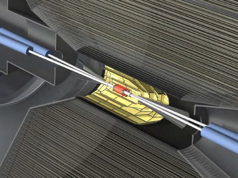
One of the goals of the Belle II experiment [1] is the improvement of the CP-violation parameter measurements made by its predecessor Belle. This makes a very precise determination of particle decay vertices necessary. For vertex measurement, Belle used four layers of double-sided silicon strip detectors in a barrel arrangement around the interaction point, called silicon vertex detector (SVD). In order to achieve a higher vertex resolution than Belle, Belle II will feature two additional layers of DEPFET [2] pixel detectors (PXD) very close to the beam pipe, surrounded by four SVD layers. This arrangement is shown in figure 1.
The inner PXD layer will have a radius of only . As a consequence of this very close proximity to the interaction point, the PXD will detect many hits from background events, mainly two-photon QED processes. The number of fired pixels per read-out cycle () from such processes will be in the order of for the whole detector, while only a small number of hits will belong to charged tracks from events relevant to the Belle II physics program. It is necessary to extract these signal hits from the much larger background, because the Belle II event builder system cannot cope with the PXD output data rate of over —more than 10 times that of all other subdetectors combined. With the PXD data alone, however, it is virtually impossible to distinguish signal hits from background hits.
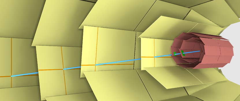
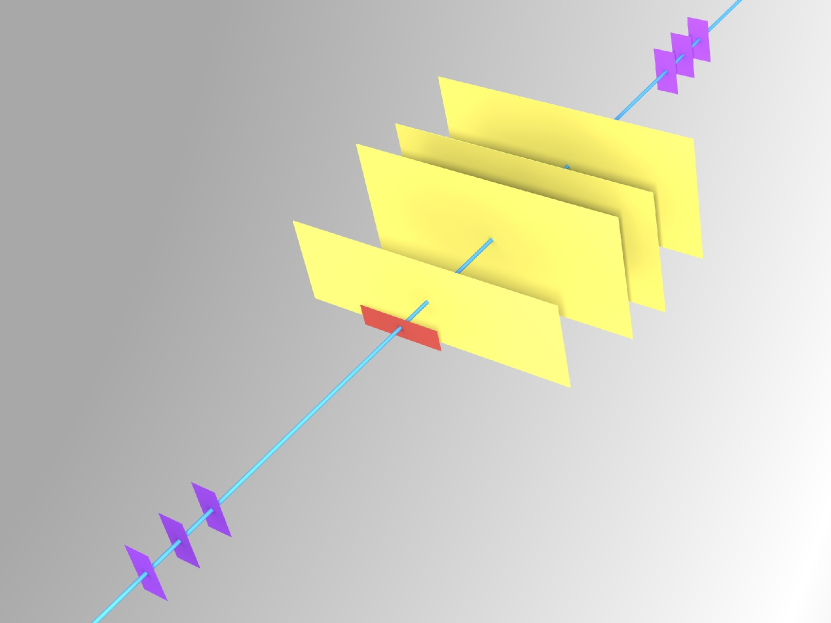
A distinction between background and signal becomes possible when data from the outer tracking detectors are taken into account: Particles produced in background processes typically have a low transversal momentum; their tracks reach the PXD, but not the SVD or the central drift chamber (CDC) surrounding it. The tracks from most relevant events, however, have a momentum high enough to reach at least the SVD. By reconstructing these tracks and finding their intercept with the layers of the PXD, rectangular areas can be determined, inside of which the corresponding hits on the PXD layers are expected. These areas are referred to as regions of interest (ROIs). The intercept of an extrapolated track with one of the PXD layers defines the center of an ROI on that layer. The ROI size depends on the uncertainty of the track reconstruction and extrapolation processes. The concept of ROI generation is illustrated in figure 2.
II Data Acquisition and ROI Generation
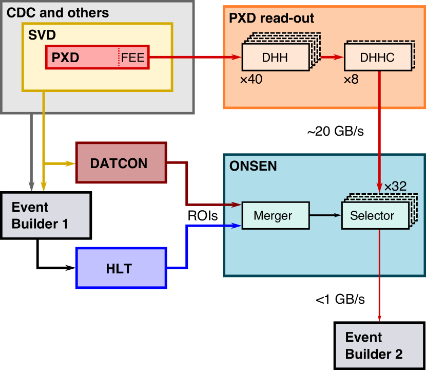
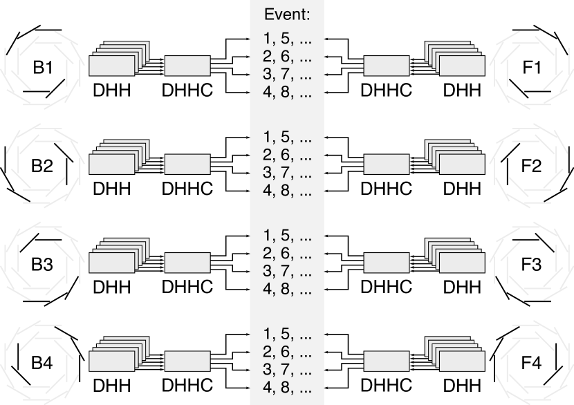
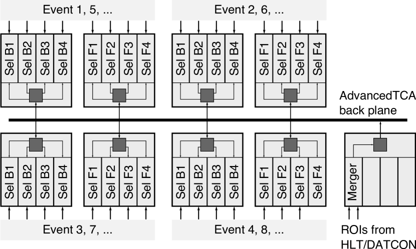
The data path for the PXD data and ROIs in Belle II is shown in figure 3. Each of the 40 PXD modules—so-called half-ladders—includes several ASICs as front-end electronics. They digitize the charge of each pixel, convert it to a zero-suppressed format, and store the digitized data in a buffer. Upon receiving a hardware trigger, a Data Handling Hybrid (DHH) [3] for each half-ladder reads these data out. The DHH is an FPGA board that is also responsible for initializing the ASICS of the half-ladder and setting configuration parameters, such as pedestal and threshold values. For every 5 DHHs, a DHH Controller (DHHC) performs a 5-to-4 multiplexing: It merges the data from 2 half-ladders of the inner PXD layer and 3 half-ladders of the outer PXD layer into a subevent (see figure 4a). Each of the 8 DHHCs then sends the merged data to the ONSEN system (see below) on one of its four output links, alternating between links on an event-by-event basis. This mechanism compensates for the higher occupancy closer to the beam pipe and effectively balances the load across the output links. The total number of output links from the PXD read-out system is 32.
Two independent subsystems of the Belle II DAQ chain create ROIs for an event:
-
1.
For events selected by the hardware triggers, the Event Builder 1 creates subevents with data from all detectors except the PXD. With this information, the high-level trigger (HLT)—a highly parallel PC farm—performs an online event reconstruction and makes a physics-level event selection (software trigger) [4]. The HLT extrapolates the tracks that were found during the event reconstruction step to the PXD and uses them for ROI generation. Depending on the event topology, a latency of up to 5 seconds is possible between the hardware trigger for an event and the response from the HLT, including software trigger and ROIs. Furthermore, the HLT output is unordered: Since the HLT processes many events in parallel, a recent event with a simple structure may already be finished, while an older, more complicated event is still being processed.
-
2.
The data concentrator (DATCON) is an FPGA-based online track reconstruction system that operates on the SVD data. The hardware platform is, for the most part, identical to that of the ONSEN system (see below). The tracking is based on a two-step approach: a sector-neighbor finder and a fast Hough transformation. The DATCON extrapolates reconstructed tracks and uses them to determine ROIs on the PXD planes, similar to the HLT. However, since it processes events in a pipelined fashion on FPGAs, the maximum processing time per event is around , and the output is ordered.
The existence of two separate ROI sources and the high latency of the HLT output make a system necessary that:
-
1.
receives and buffers the data output from the PXD;
-
2.
receives and buffers the ROIs generated by the DATCON;
-
3.
receives software triggers and ROIs from the HLT;
-
4.
matches all ROIs and data for an event as soon as the HLT ROIs have arrived; and
-
5.
performs the actual pixel data reduction, based on the combined ROIs from both sources.
The hardware platform for such a system must meet certain requirements, including: fast optical serial links for the reception of PXD data; gigabit Ethernet interfaces for both the reception of the software trigger and ROIs and the output of the reduced data; large memory, allowing the buffering of the PXD data; high memory and I/O bandwidth; and high-speed data processing capabilities.
III The ONSEN System
The Online Selection Nodes (ONSEN) system was developed to fulfill the requirements stated above. An earlier version of the system was described in a previous publication [5]. The hardware platform has since been upgraded, and many changes were made to data formats, implementation specifics, and the overall data flow concept. The new system was tested extensively in both laboratory and beam tests.
III-A Hardware
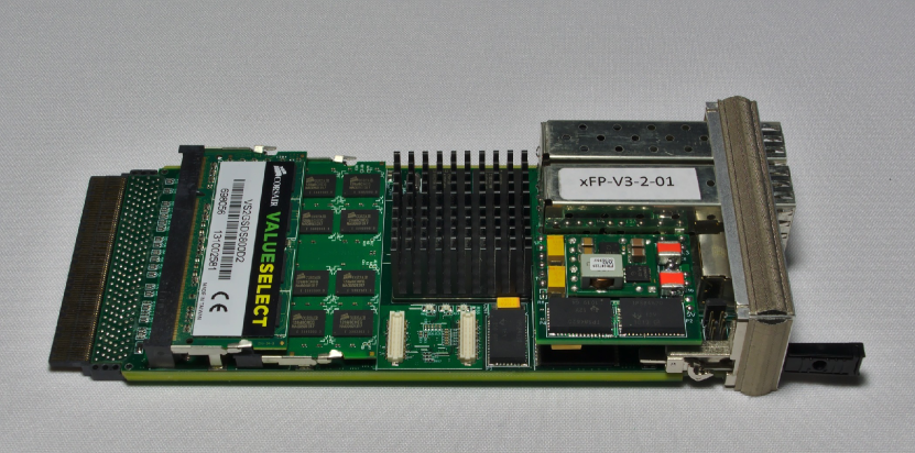
The hardware platform for the ONSEN system will consist of 33 xTCA-based FPGA Processor (xFP) cards [6] hosted by 9 AdvancedTCA carrier boards. It is a development of IHEP Beijing in collaboration with JLU Giessen. Figure 5a shows an xFP card of the third hardware revision. This is the final version, which will be used in the Belle II experiment. It features a Xilinx Virtex-5 FX70T FPGA with an embedded PowerPC CPU. Two DDR2 modules provide of RAM—enough to store the output of one DHHC for at least five seconds. An RJ45 port, used with the embedded Ethernet MAC of the Virtex-5, provides gigabit Ethernet connectivity. Four SFP+ cages connect to multi-gigabit serial transceivers of the FPGA. They can be equipped with different pluggable modules, each adding either an optical fiber interface, running at up to , or an additional RJ45 socket for gigabit Ethernet. Six more multi-gigabit transceivers are routed to the module’s AMC connector.
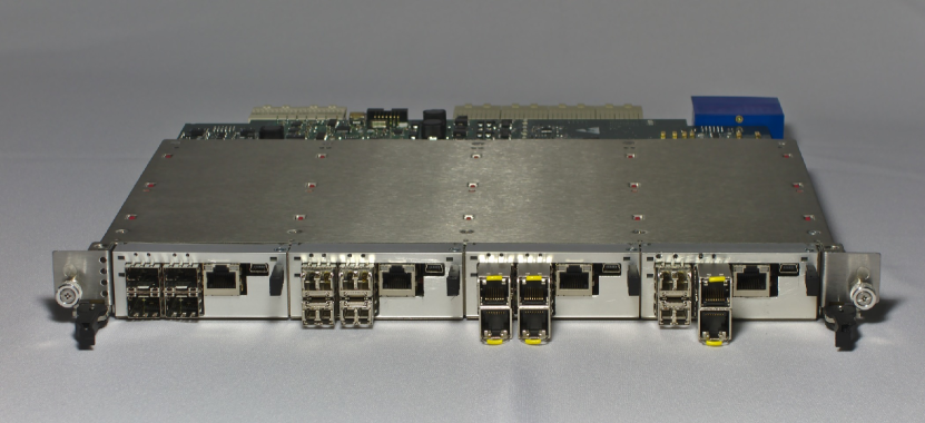
Figure 5b shows the “Compute Node” carrier board. It hosts four xFP cards and establishes a full-mesh interconnection between them, using the multi-gigabit links on the AMC connectors. In addition, the carrier board features a Virtex-4 FX60 FPGA that connects to the AdvancedTCA back plane with 16 multi-gigabit links and to each xFP card with four duplex LVDS ports. This FPGA acts as a switch: When multiple carrier boards, each equipped with one or more xFP cards, are used together in an AdvancedTCA shelf, the switch FPGAs allow the xFP cards to communicate with each other. Figure 4b shows how these channels will be employed in the ONSEN system for the distribution of ROIs in the system. This mechanism will be explained in more detail below.
III-B Implementation
Using the information from the HLT, the ONSEN system achieves the required data reduction factor of 30 in two steps: A positive software trigger decision is expected for about one-third of all events. If the HLT rejects an event, the ONSEN system discards all corresponding pixel data. This happens regardless of possible ROIs found by the DATCON, since the data from the other subdetectors is lost in case of a rejected trigger. By this mechanism, the software trigger reduces the average trigger rate from to , effectively dividing the output data rate by 3.
The ROIs for accepted events will cover approximately 1/10 of the sensitive PXD area. Since most PXD hits stem from background events, the ONSEN system reduces the output data rate by another factor of 10 by discarding hits that are not inside ROIs.
Two pairs of FPGA configurations for the 33 xFP cards and their associated carrier boards will be used in the ONSEN system:
-
1.
One of the 33 xFP cards acts as the merger node. It receives ROIs from the DATCON via optical fiber and stores them in RAM. A pointer to the stored information, along with the corresponding event number, is written to a look-up table. The merger node then waits for the HLT to send a software trigger decision, and possibly ROIs, for the same event. The connection between HLT and merger node is established via gigabit Ethernet, using an RJ45 SFP+ transceiver. As transport layer protocol, an FPGA implementation of either TCP (namely SiTCP [7]) or UDP will be used.
Upon receiving the software trigger decision and HLT ROIs for an event, the merger node reads back the corresponding DATCON ROIs from memory. It combines the ROIs from both sources into a single packet and transfers it to the switch FPGA on the carrier board.
The switch FPGA uses the back plane of the AdvancedTCA shelf to distribute the ROI packets to the other boards in the ONSEN system, which perform the actual selection of the pixel data. The switch FPGA performs a preselection: It only distributes the relevant ROI packets (i.e., those for the associated event numbers) to each of the other carrier boards. The preliminary mapping of PXD sections and event numbers to the individual boards in the ONSEN system is shown in figure 4b.
-
2.
The remaining 32 xFP cards are the selector nodes. They populate 8 carrier boards in groups of 4. Each selector node is connected to one of the output links of a DHHC via a optical fiber link. It receives the data from one of the eight PXD sections for one out of every four events. Eight selector nodes cover all sections of the PXD, so that the cards hosted by two carrier boards process the data for a complete event.
When a selector node receives the PXD data for an event, it writes them to RAM and stores the pointer and event number in a look-up table (much like the merger node does for the DATCON ROIs). After no more than 5 seconds, the merger node will have received and processed an HLT packet for the same event, and its switch FPGA will have distributed it over the AdvancedTCA back plane. The other switch FPGAs receive these packets and distribute them to the selector nodes. When the ROIs for an event arrive, the selector nodes read back the relevant pixel data from memory, filter them according to the ROI information, and send the reduced data to the Belle II Event Builder 2. For this connection, again, an RJ45 SFP+ transceiver and either SiTCP or UDP are used.
The logic for both merger and selector nodes has been implemented in VHDL and tested extensively. A Linux system, running on the embedded CPUs in the FPGAs of the xFP cards and carrier boards, is used for debugging, monitoring, and online configuration of the ONSEN system. It can be accessed over gigabit Ethernet via the RJ45 ports on the front panel of the xFP cards. Slow control functions of the FPGA logic are made available through registers on an embedded bus system. They are accessible via an EPICS daemon [8] running on the Linux system. This configuration allows the integration of the ONSEN system into the overall Belle II slow control scheme.
IV Beam Test in January 2014
During a four-week test at the DESY test beam facility in January 2014, modules of the Belle II PXD and SVD were used in conjunction for the first time. The setup for this test included a “radial slice” of the vertex detector: one PXD layer and four SVD layers, allowing to exercise data acquisition with both systems as well as online track reconstruction, ROI generation, data reduction, and event building. Figure 6 shows the detector configuration that was used during most runs: Beside the PXD and SVD modules, six layers of the EUDET pixel detector [9], available at the DESY test beam facility, were included as a “beam telescope” for alignment and verification purposes.
The momentum and rate of the electron or positron beam available in the test beam area could be varied by choosing different conversion targets, currents for the beam spread magnet, and collimator settings. Momenta of up to and rates of up to were available.
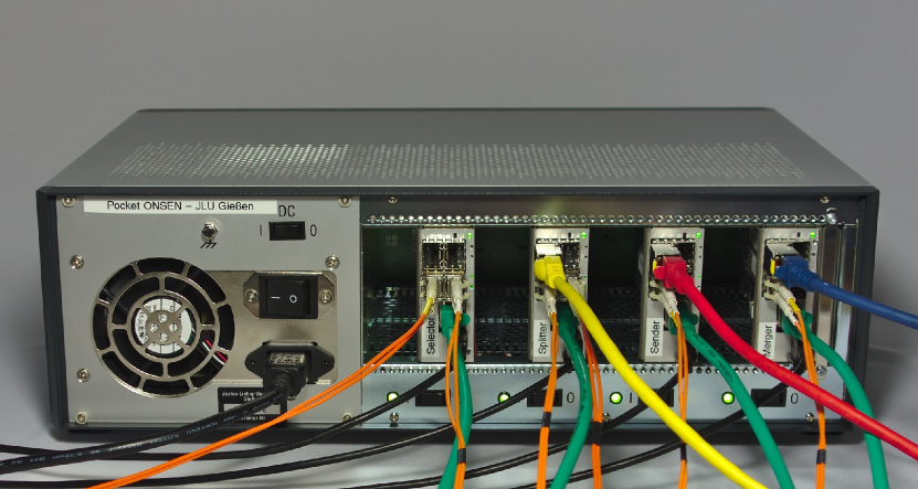
A scaled-down but fully functional “Pocket DAQ” system was set up for this test, including the HLT and event builder systems. Similarly, a “Pocket ONSEN” system was used to exercise the data reduction mechanism (see figure 7): Instead of an AdvancedTCA shelf with carrier boards, a MicroTCA shelf with individual xFP cards was used, allowing direct connections between the boards through the back plane without an intermediate switch.
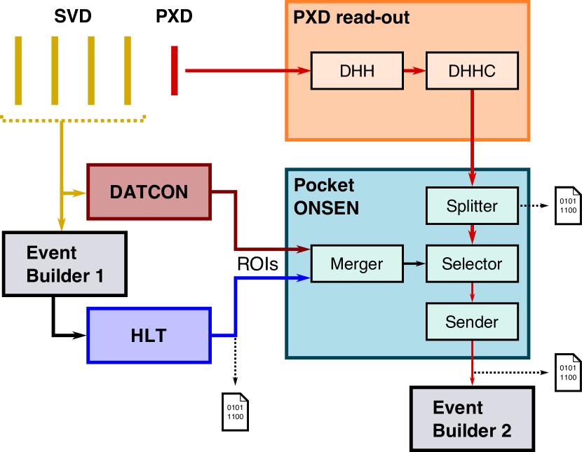
Figure 8 shows the data flow scheme of PXD and SVD data during the beam test. All subsystems relevant for the data acquisition were present (compare figure 3). For the read-out of the single PXD half-ladder, one DHH and one DHHC were required. The Pocket ONSEN system included a merger node and a selector node. Both modules had all core functions required in the final Belle II system, including: I/O, memory access, pointer handling, pixel data reduction, and basic slow control. Two additional modules were used in this test:
-
1.
An optional splitter node was inserted in the data path between the DHHC and the selector node. It forwarded the pixel data to the selector node and, in addition, forked it to a gigabit Ethernet output. A PC could be used to receive this data stream and save it to a file.
-
2.
The extensive use of debugging features in the selector nodes (mainly integrated logic analyzer cores) reduced the available FPGA resources. The considerable size of the SiTCP core therefore made it necessary to offload the gigabit Ethernet output of the reduced pixel data from the selector to an additional sender node. From selector to sender node, data was transferred via optical fiber.
The file forked from the splitter node contained the complete PXD output data, packed into a convenient data format by the PXD read-out system. Since this data was yet untouched by the actual data reduction mechanism, the file could be used for offline verification of the ONSEN system. In a similar fashion, the data output after the sender module (i.e., the PXD data after data reduction) and the output from the HLT (i.e., software trigger and ROI packets) were saved by inserting a PC in the Ethernet data stream between HLT, Pocket ONSEN, and Event Builder 2. That way, all input and output data streams of the ONSEN system (for runs in which the DATCON was not used) were recorded. By analyzing these files, it was possible to check whether the PXD hits were correctly forwarded or discarded by the ONSEN system.
A first connection test of the data acquisition chain included only the HLT, Pocket ONSEN, and Event Builder 2. Random triggers were generated at varying rates, for which the HLT created software trigger packets. It was verified that the merger and selector modules in the ONSEN system processed these packets correctly: Without PXD data for the triggers, the data from the HLT were packed in the ONSEN output format and passed through to the Event Builder 2, which was able to parse them and extract the correct trigger number. Besides validating the data transport mechanism and format consistency between the various DAQ subsystems, it could be shown that trigger rates of —more than the available test beam rates—could be handled by all systems. Note that this limit was not imposed by the ONSEN system; previous laboratory tests, using “dummy” data and trigger inputs, confirmed that the ONSEN system can cope with event rates above the final Belle II average trigger rate of .
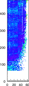
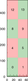
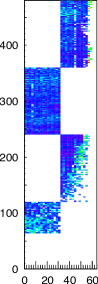
After the installation of the detectors and read-out systems in the test beam areas, first runs were taken with fixed ROI patterns. In particular, ROIs covering the entire PXD matrix were sent to the ONSEN system, so that no hits were discarded. After the complete DAQ chain had been established, noise data from the PXD (without beam and pedestal configuration) was recorded with varying ROI patterns. Figure 9 shows the results from such a run, which was used for a rough sanity check of the ONSEN system: It was shown that the ONSEN output only included PXD hits inside areas selected by ROIs.
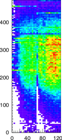
The first data taken with beam and “full frame” ROIs allowed the alignment of the various detector layers. The next step was the verification of the tracking algorithm and generation of real ROIs [10]. Figure 10 shows a hit map of data taken with real ROIs, after data reduction performed by the ONSEN system.
Altogether, more than 20 million events were recorded with all essential subsystems of the DAQ chain. An analysis of the recorded ONSEN input and output data files shows that the ONSEN system worked without errors: For all recorded events, all pixel hits selected by ROIs were sent to the Event Builder 2, and all other hits were discarded.
V Conclusion and Outlook
The ONSEN data reduction system is an essential part of the data acquisition system for the Belle II pixel detector. During the combined beam test of the Belle II vertex detector in January 2014, we showed that the ONSEN system is in a mature state, both in terms of hardware and FPGA firmware. The production of the remaining modules for the system is currently ongoing. Installation will start in 2015.
Acknowledgment
The authors would like to thank G. Korcyl of the Jagiellonian University, Kraków, for providing us with his FPGA implementation of the UDP protocol and for his continuing support in this regard.
References
- [1] T. Abe et al., “Belle II Technical Design Report,” ArXiv e-prints, Nov. 2010.
- [2] R. Richter et al., “Design and technology of DEPFET pixel sensors for linear collider applications,” Nucl. Instrum. Meth. A, vol. 511, no. 1–2, pp. 250–256, 2003.
- [3] D. Levit et al., “FPGA based data read-out system of the Belle II pixel detector,” presented at the 19th IEEE-NPSS Real Time Conf., Nara, Japan, May 2014.
- [4] R. Itoh, T. Higuchi, M. Nakao, S. Suzuki, and S. Lee, “Data flow and high level trigger of Belle II DAQ system,” IEEE Trans. Nucl. Sci., vol. 60, no. 5, pp. 3720–3724, Oct 2013.
- [5] B. Spruck et al., “The Belle II pixel detector data acquisition and reduction system,” IEEE Trans. Nucl. Sci., vol. 60, no. 5, pp. 3709–3713, Oct 2013.
- [6] J. Zhao et al., “A general xTCA compliant and FPGA based data processing building blocks for trigger and data acquisition system,” presented at the 19th IEEE-NPSS Real Time Conf., Nara, Japan, May 2014.
- [7] T. Uchida, “Hardware-based TCP processor for gigabit Ethernet,” IEEE Trans. Nucl. Sci., vol. 55, no. 3, pp. 1631–1637, June 2008.
- [8] Experimental physics and industrial control system. [Online]. Available: {http://www.aps.anl.gov/epics}
- [9] I. Rubinskiy, “An EUDET/AIDA pixel beam telescope for detector development,” Phys. Procedia, vol. 37, no. 0, pp. 923–931, 2012.
- [10] E. Paoloni et al., “Demonstrator of the Belle2 online tracking and pixel data reduction on the high level trigger system,” presented at the 19th IEEE-NPSS Real Time Conf., Nara, Japan, May 2014.