Fermi-edge transmission resonance in graphene driven by a single Coulomb impurity
Abstract
The interaction between the Fermi sea of conduction electrons and a non-adiabatic attractive impurity potential can lead to a power-law divergence in the tunneling probability of charge through the impurity. The resulting effect, known as the Fermi edge singularity (FES), constitutes one of the most fundamental many-body phenomena in quantum solid state physics. Here we report the first observation of FES for Dirac Fermions in graphene driven by isolated Coulomb impurities in the conduction channel. In high-mobility graphene devices on hexagonal boron nitride substrates, the FES manifests in abrupt changes in conductance with a large magnitude at resonance, indicating total many-body screening of a local Coulomb impurity with fluctuating charge occupancy. Furthermore, we exploit the extreme sensitivity of graphene to individual Coulomb impurities, and demonstrate a new defect-spectroscopy tool to investigate strongly correlated phases in graphene in the quantum Hall regime.
Experimental observation of interaction-driven many-body phenomena in graphene depends critically on background disorder, which in mechanically exfoliated graphene arises primarily from the trapped Coulomb impurities at the substrate or at the surface (adatoms or adsorbates) Castro Neto et al. (2009); Chen et al. (2008). The discovery of the fractional quantum Hall effect Du et al. (2009); Bolotin et al. (2009), broken symmetry states at zero filling factor Weitz et al. (2010), or spin-valley quantum Hall ferromagnetism Young et al. (2012), have all been achieved in high mobility suspended graphene devices or graphene on hexagonal boron nitride (hBN) substrates, where the influence of external disorder was minimized. However, the ability of graphene to screen an external impurity potential, not only determines the strength of electron-electron interaction and related physical properties such as the dielectric constant Wang et al. (2012) or the Fermi velocity Elias et al. (2011), it also induces another class of many body effects such as the Anderson orthogonality catastrophe Anderson (1967); Hentschel and Guinea (2007), local moment formation Uchoa et al. (2008); Cornaglia et al. (2009) and the Kondo effect Sengupta and Baskaran (2008); Chen et al. (2011); Dóra and Thalmeier (2007). This latter class of phenomena, where disorder itself plays a central role, remains poorly explored in graphene.
Some experimental attempts have now been made to probe many-body effects induced by disorder in graphene. These include scanning tunneling spectroscopy of isolated Coulomb impurities adsorbed on graphene Wang et al. (2012); Brar et al. (2011); Luican-Mayer et al. (2014), and quantum transport via localized states created by ion irradiation Chen et al. (2011). However, the structural integrity of graphene in the latter can be affected too adversely to identify many-body effects unambiguously. In this letter we report a striking new phenomenon in the electrical transport in high-mobility graphene, on hBN, which manifests in random telegraph switching in the electrical conductance with a large magnitude of at resonance. The switching is observable only within restricted windows of gate voltage, and the analysis of the switching rates suggests tunneling of charge, driven by attractive Coulomb interaction between the Dirac Fermions in graphene and unintentional Coulomb impurities located near one of the metallic contacts. We suggest that this remarkable effect represents the first evidence of a many-body transmission resonance via Fermi-edge singularity in graphene. Although FES is immensely important to many phenomena including X-ray absorption Ohtaka and Tanabe (1990), Kondo effect Anderson et al. (1970); Andrei et al. (1983) and transport in mesoscopic systems Cobden and Muzykantskii (1995); Geim et al. (1994), it has thus far never been observed in graphene, where the Dirac-fermionic charge carriers may play a nontrivial role Hentschel and Guinea (2007).
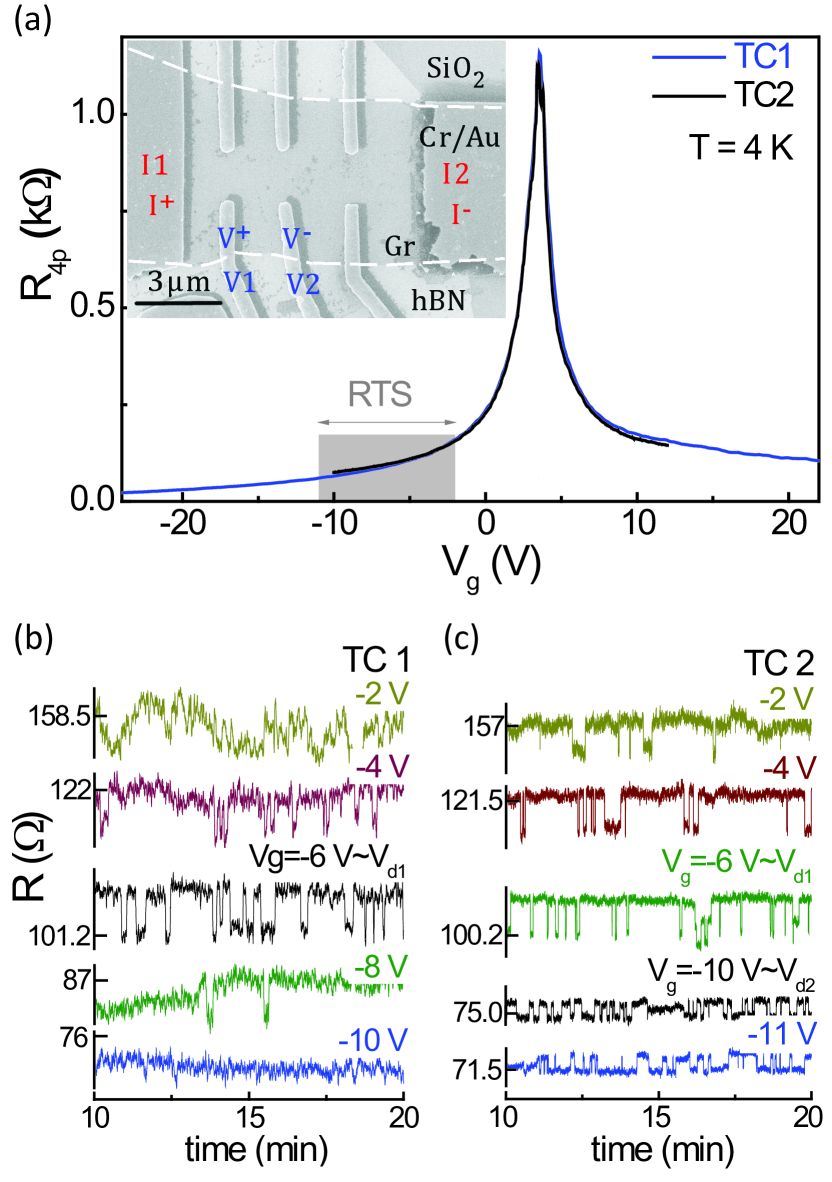
The graphene transistor explored in detail in this experiment was prepared on a hBN substrate, closely following the approach in Zomer et al. (2011). Details of the fabrication procedure can be found in the supplementary section. Fig. 1a (inset) shows an electron microscope image of the device used in our experiments. Resistance () vs. back gate voltage () characteristics shown in Fig. 1a reveal electron and hole mobility to be cm2/Vs and cm2/Vs, respectively. All measurements are carried out at K, with a small source-drain bias, , such that the system is maintained in thermal equilibrium. The key result of this work is the unexpected observation of a random telegraph signal (RTS) in (current leads: I1-I2, voltage leads: V1-V2 in Fig. 1a) as a function of time, detectable only over a certain range (shaded region in Fig. 1a). For low close to the Dirac point, the RTS becomes hard to isolate from the background noise, while for V the amplitude of the RTS was too small to detect. This explains why most earlier noise studies Pal et al. (2011, 2010); Pal and Ghosh (2009a); Pal and Ghosh (2009b) in low or moderate mobility graphene failed to explore the RTS in detail, where large noise dominates resistivity noise over a wide range of gate voltage ( V) on either side of the Dirac point.
In this experiment, we subject the device to several thermal cycles between K and K. This does not affect the characteristics significantly, but modifies the RTS characteristics. This is illustrated with two of the thermal cycles, denoted as TC1 and TC2 in Fig. 1, in which the RTS noise was most pronounced. The local enhancement of RTS amplitude and switching rate in both TC1 and TC2 (Fig. 1b, c) indicates a resonant defect level around V. An additional level appears at more negative for TC2 (Fig. 1c), causing detectable switching noise down to V. The observation of RTS in high-mobility graphene transistors is an important result, as it implies that its electrical properties can be significantly modified even by a single charge trap or impurity.
RTS has often been observed due to carrier number fluctuation in nanoscale or mesoscopic semiconductors with small number of carriers Kirton and Uren (1989), but this model fails here as the observed RTS amplitude ( %) is more than two orders of magnitude larger than the expected for charge exchange with a single defect at (hole) doping of cm-2 ( V). Mobility fluctuation due to a single two-level trap-state is not only a physically unlikely scenario, but it also yields assuming a reasonable Hooge parameter of Pal et al. (2011); Pal and Ghosh (2009b); Pal et al. (2010); Pal and Ghosh (2009a). Finally, no RTS is observed when voltage leads other than V1 are used to measure (see supplementary material for details), allowing us to conclude that the observed RTS is not intrinsic to graphene and is observed only when the Fermi energy of graphene aligns with the discrete energy level of a defect or impurity that is located close to the lead V1 (see schematic in Fig. 2c), presumably incorporated unintentionally during device fabrication.
Experiments with small silicon MOSFETs Cobden and Muzykantskii (1995) show that strong RTS can also occur due to intermittent occupancy fluctuation of an impurity in proximity to the conducting 2D channel where the channel and the charged impurity interact via an attractive Coulomb potential. When the impurity state is resonant with the Fermi energy of the channel, the interaction screens the charged impurity by forming a many-body bound state. This causes a power-law singularity Matveev and Larkin (1992), called the Fermi edge singularity, in the tunneling probability between the impurity state and the 2D channel, in a manner that is analogous to the Kondo effect with localized spins. Effectively, the interaction adds one conduction channel via the impurity state which, in the unitary limit, increases conductance by as much as (where is the level degeneracy) compared to when the impurity is neutral or repulsive.
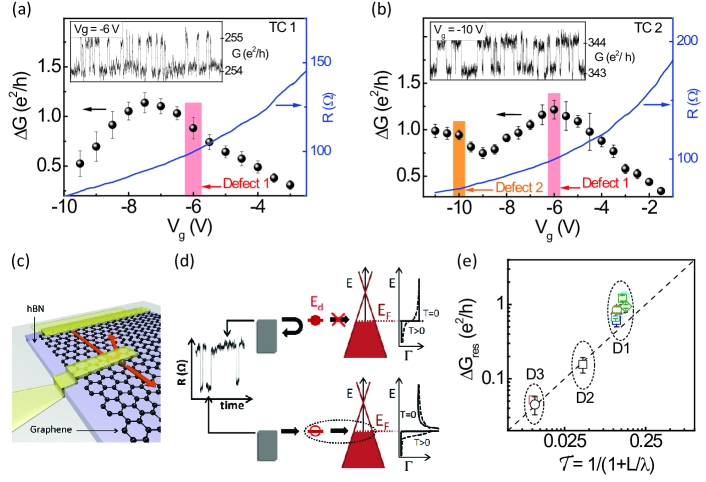
To explore this possibility in our devices, we analyze the RTS amplitude as a function of for both thermal cycles. The time series in the insets of Figs. 2a and 2b demonstrate the RTS to correspond to change in conductance at both resonances ( V and V). Figs. 2a and 2b show the average as a function of , where and are the high and low resistance states of the RTS, respectively. varies nonmonotonically with , and peaks at V (TC1 and TC2) and V (TC2), confirming the resonance-like behavior. Strikingly, the magnitude of the conductance change at resonance, is , and remains similar at all resonances, irrespective of impurity-specific details such as its location and coupling to graphene. Such a universality readily rules out a non-interacting mechanism of resonant tunnelling between the impurity state and graphene, but suggests a many-body effect with singular quasiparticle tunneling.
For a quantitative microscopic framework we assume screening of a Coulomb impurity located at the peripheral region of lead V1 (Fig. 2c). Intermittent tunneling out of a hole (i.e. capturing of an electron) causes a fluctuating attractive Coulomb potential between the impurity and the 2D hole gas in graphene. As schematically described in Fig. 2d, this corresponds to a time-dependent two-state fluctuation in the “contact” resistance, as the quasi-bound state of the charged defect and graphene incorporate one additional conduction channel. Including the scattering of carriers between the voltage leads, the net expected conductance change at resonance can be expressed as , where , is the transmission probability of charge between the leads Datta (1997). Here is the mean free path which can be readily estimated from the characteristics (see supplementary material for details), and is the separation between the leads.
In Fig. 2e we have compiled the measured against the experimentally estimated for all resonances observed in three different graphene devices. For the present high mobility device (D1), we observed 11 resonances spanning a range of V to V corresponding to ( nm), over all the thermal cycles. In addition, we performed a similar analysis for two other devices, denoted as D2 and D3, where graphene was deposited directly on the SiO2 substrate. The carrier mobility ( cm2/Vs) in these two devices is significantly lower, corresponding to nm, and they also displayed strongly suppressed (details of these devices and calculations can be found in the supplementary section). Most remarkably, as shown in Fig. 2e, the variation of the measured at all resonances in different devices falls close to (dashed line) with , arising from the two-fold spin and valley degeneracy in graphene. This result emphasizes that RTS due to interacting Coulomb impurities could be generic to graphene field-effect devices which, counterintuitively, becomes stronger as the mobility of the channel is increased.
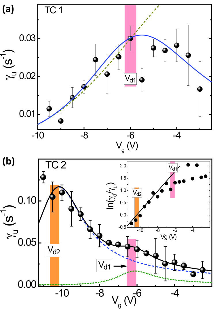
To further verify the role of interaction, we compute the emission () and capture () rate of charge (hole) from the defect state as the inverse lifetimes of the and resistance states, respectively (see Fig. 2d and supplementary material). In Fig. 3a and 3b we have plotted the dependence of on for thermal cycles TC1 and TC2, respectively. The -dependence of for thermal cycles TC1 and TC2 is shown in the supplementary material. The clear non-monotonic dependence of on confirms the failure of the non-interacting framework. In fact, we find that follows the singular transmission probabilities generalized for finite temperature (Fig. 3a, b) Cobden and Muzykantskii (1995); Matveev and Larkin (1992),
| (1) |
where to the leading order, with and being the defect energy and corresponding gate voltage, respectively. The parameter couples the energy difference to the offset in , and is obtained directly from the slope of as a function of in the vicinity of the resonances Cobden and Muzykantskii (1995), as shown in the inset of Fig. 3b. The analysis contains two fit parameters: (1) The defect potential , which was expectedly found close to the corresponding to and for each resonance, and (2) the interaction parameter , which was found to be for both resonances and thermal cycles. The interaction parameter governs the singularity in transition rate , and is a direct measure of the Coulomb interaction between the defect state and graphene ( represents the non-interacting case). The observed suggests a weak screening by graphene in spite of reasonably high doping ( cm-2) Hentschel and Guinea (2007). This is supported by the recent observation of low dielectric constant of graphene even on hBN substrates Wang et al. (2012), and affirms the importance of including electron-electron interaction in evaluating physical properties of graphene.
It is essential to comment on two key aspects of our experiment: First, the Coulomb impurities in our device can arise from both structural imperfections (such as edge defects or vacancies) or surface adsorbates, in particular transition metal adatoms, such as Cr or Au, perhaps incorporated during metallization. The latter scenario is supported by (1) proximity of the active impurities to one of the leads (voltage lead V1), and (2) occupation fluctuations of the 3d atomic clusters (cobalt trimers) adsorbed on graphene have been shown to occur in a similar range of gate voltage Wang et al. (2012). Secondly, resonances arising from bound state formation with singly charged impurities via atomic collapse can also be important Hentschel and Guinea (2007); Wang et al. (2013) considering a low dielectric constant for graphene Wang et al. (2012). However, the RTS we observe does not exhibit features exclusive to the Dirac fermions.
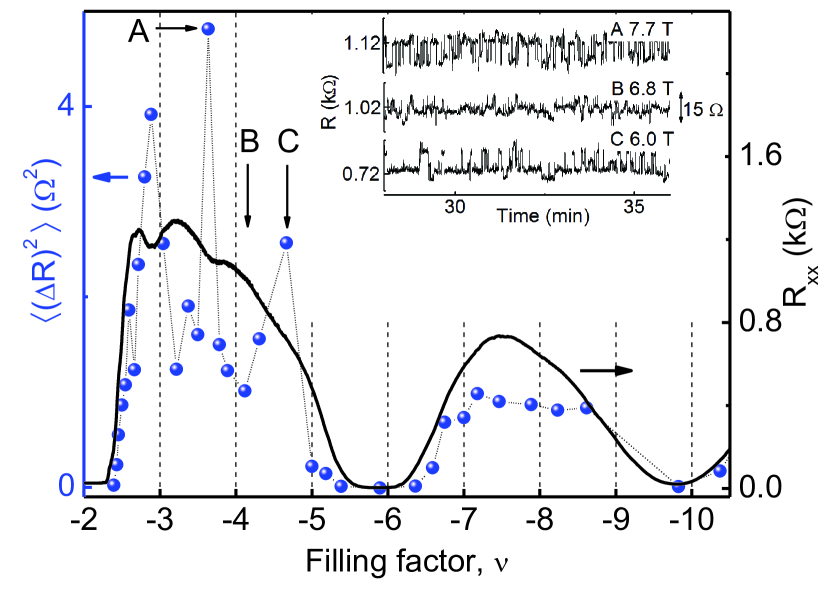
Subsequently, we employ the tunnel coupling between the Coulomb impurity and graphene as a spectroscopic tool to explore the Landau level (LL) structure in the integer quantum Hall regime, where Coulomb (exchange) interaction may result in new broken symmetry states Nomura and MacDonald (2006); Young et al. (2012); Weitz et al. (2010); Feldman et al. (2012). The proximity of the impurity to the graphene channel makes defect spectroscopy an extremely sensitive probe to the local density of states (LDOS) Main et al. (2000); Schmidt et al. (1997). In the experiment here, we measured the RTS at different magnetic fields (perpendicular to the plane of graphene) in the quantum Hall regime while keeping the Fermi level fixed at V (see typical traces in the inset of Fig. 4). The RTS in the quantum Hall regime differ strongly from the zero case and we find: (1) strong modulation in resulting from the wide variation in LDOS with , (2) appearance of multilevel structures, and (3) enhanced switching rate with multiple characteristic rates. The overall variance of the resistance, , was found to follow the Shubnikov-de Haas oscillations in longitudinal resistance, , (Fig. 4) confirming that the RTS is indeed sensitive to the LDOS, and that the RTS amplitude drops sharply when the Fermi energy moves to a gap Cobden and Muzykantskii (1995).
The striking observation in Fig. 4 is the clear suppression of the RTS [minima in ] at filling factor and -4 in the first LL, and moderately at and -8 in the second LL (the data at was corrupted during the measurements), suggesting removal of the four-fold spin-valley degeneracy even at as low as T. The averaged resistance, shows significantly weaker features at these fields establishing the superior sensitivity of single-defect noise spectroscopy in probing the LDOS. Recent transport experiments at high magnetic fields attributed the lifting of degeneracy at half and quarter fillings to an exchange-driven quantum Hall ferromagnetism in the SU(4) spin-valley space Young et al. (2012). The observation that the noise magnitude indicates lifting of degeneracy, at these filling factors, even for Zeeman energy , confirms strong orbital effect of Coulomb interaction in forming the gaps.
In conclusion, we have observed a new transmission resonance in high-mobility graphene transistors, which manifests as a random telegraph signal in conductance with amplitude as large as . Our analysis suggests this to be due to Fermi edge singularity caused by bound state formation between a local Coulomb impurity and charge carriers in graphene. Apart from demonstrating a new many-body quantum state in graphene, driven by individual Coulomb impurities, we have also employed this phenomenon to probe the modification in the local density of states of graphene by Coulomb interaction in the integer quantum Hall regime.
We thank Andre Geim for useful discussions. S.G. thanks the IISc Centenary Postdoctoral Fellowship for financial support. V.K. and A.N.P. thank CSIR for financial support. The authors thank the Department of Science and Technology for financial support.
References
- Castro Neto et al. (2009) A. H. Castro Neto, F. Guinea, N. M. R. Peres, K. S. Novoselov, and A. K. Geim, Rev. Mod. Phys. 81, 109 (2009).
- Chen et al. (2008) J.-H. Chen, C. Jang, S. Adam, M. S. Fuhrer, E. D. Williams, and M. Ishigami, Nat Phys 4, 377 (2008).
- Du et al. (2009) X. Du, I. Skachko, F. Duerr, A. Luican, and E. Y. Andrei, Nature 462, 192 (2009).
- Bolotin et al. (2009) K. I. Bolotin, F. Ghahari, M. D. Shulman, H. L. Stormer, and P. Kim, Nature 462, 196 (2009).
- Weitz et al. (2010) R. T. Weitz, M. T. Allen, B. E. Feldman, J. Martin, and A. Yacoby, 330, 812 (2010).
- Young et al. (2012) A. F. Young, C. R. Dean, L. Wang, H. Ren, P. Cadden-Zimansky, K. Watanabe, T. Taniguchi, J. Hone, K. L. Shepard, and P. Kim, Nat Phys 8, 550 (2012).
- Wang et al. (2012) Y. Wang, V. W. Brar, A. V. Shytov, Q. Wu, W. Regan, H.-Z. Tsai, A. Zettl, L. S. Levitov, and M. F. Crommie, Nat Phys 8, 653 (2012).
- Elias et al. (2011) D. C. Elias, R. V. Gorbachev, A. S. Mayorov, S. V. Morozov, A. A. Zhukov, P. Blake, L. A. Ponomarenko, I. V. Grigorieva, F. Novoselov, K. S.and Guinea, and A. K. Geim, Nat Phys 7, 701 (2011).
- Anderson (1967) P. W. Anderson, Phys. Rev. Lett. 18, 1049 (1967).
- Hentschel and Guinea (2007) M. Hentschel and F. Guinea, Phys. Rev. B 76, 115407 (2007).
- Uchoa et al. (2008) B. Uchoa, V. N. Kotov, N. M. R. Peres, and A. H. Castro Neto, Phys. Rev. Lett. 101, 026805 (2008).
- Cornaglia et al. (2009) P. S. Cornaglia, G. Usaj, and C. A. Balseiro, Phys. Rev. Lett. 102, 046801 (2009).
- Sengupta and Baskaran (2008) K. Sengupta and G. Baskaran, Phys. Rev. B 77, 045417 (2008).
- Chen et al. (2011) J.-H. Chen, L. Li, W. G. Cullen, E. D. Williams, and M. S. Fuhrer, Nat Phys 7, 535 (2011).
- Dóra and Thalmeier (2007) B. Dóra and P. Thalmeier, Phys. Rev. B 76, 115435 (2007).
- Brar et al. (2011) V. W. Brar, R. Decker, H.-M. Solowan, Y. Wang, L. Maserati, K. T. Chan, H. Lee, C. O. Girit, A. Zettl, S. G. Louie, et al., Nat Phys 7, 43 (2011).
- Luican-Mayer et al. (2014) A. Luican-Mayer, M. Kharitonov, G. Li, C.-P. Lu, I. Skachko, A.-M. B. Gonçalves, K. Watanabe, T. Taniguchi, and E. Y. Andrei, Phys. Rev. Lett. 112, 036804 (2014).
- Ohtaka and Tanabe (1990) K. Ohtaka and Y. Tanabe, Rev. Mod. Phys. 62, 929 (1990).
- Anderson et al. (1970) P. W. Anderson, G. Yuval, and D. R. Hamann, Phys. Rev. B 1, 4464 (1970).
- Andrei et al. (1983) N. Andrei, K. Furuya, and J. H. Lowenstein, Rev. Mod. Phys. 55, 331 (1983).
- Cobden and Muzykantskii (1995) D. H. Cobden and B. A. Muzykantskii, Phys. Rev. Lett. 75, 4274 (1995).
- Geim et al. (1994) A. K. Geim, P. C. Main, N. La Scala, L. Eaves, T. J. Foster, P. H. Beton, J. W. Sakai, F. W. Sheard, M. Henini, G. Hill, et al., Phys. Rev. Lett. 72, 2061 (1994).
- Zomer et al. (2011) P. J. Zomer, S. P. Dash, N. Tombros, and B. J. van Wees, Applied Physics Letters 99, 232104 (2011).
- Pal et al. (2011) A. N. Pal, S. Ghatak, V. Kochat, E. S. Sneha, A. Sampathkumar, S. Raghavan, and A. Ghosh, ACS Nano 5, 2075 (2011).
- Pal et al. (2010) A. N. Pal, A. A. Bol, and A. Ghosh, Applied Physics Letters 97, 133504 (2010).
- Pal and Ghosh (2009a) A. N. Pal and A. Ghosh, Applied Physics Letters 95, 082105 (2009a).
- Pal and Ghosh (2009b) A. N. Pal and A. Ghosh, Phys. Rev. Lett. 102, 126805 (2009b).
- Kirton and Uren (1989) M. Kirton and M. Uren, Advances in Physics 38, 367 (1989).
- Matveev and Larkin (1992) K. A. Matveev and A. I. Larkin, Phys. Rev. B 46, 15337 (1992).
- Datta (1997) S. Datta, Electronic transport in mesoscopic systems (Cambridge university press, 1997).
- Wang et al. (2013) Y. Wang, D. Wong, A. V. Shytov, V. W. Brar, S. Choi, Q. Wu, H.-Z. Tsai, W. Regan, A. Zettl, R. K. Kawakami, et al., Science 340, 734 (2013).
- Nomura and MacDonald (2006) K. Nomura and A. H. MacDonald, Phys. Rev. Lett. 96, 256602 (2006).
- Feldman et al. (2012) B. E. Feldman, B. Krauss, J. H. Smet, and A. Yacoby, 337, 1196 (2012).
- Main et al. (2000) P. C. Main, A. S. G. Thornton, R. J. A. Hill, S. T. Stoddart, T. Ihn, L. Eaves, K. A. Benedict, and M. Henini, Phys. Rev. Lett. 84, 729 (2000).
- Schmidt et al. (1997) T. Schmidt, R. J. Haug, V. I. Fal’ko, K. v. Klitzing, A. Förster, and H. Lüth, Phys. Rev. Lett. 78, 1540 (1997).