Ion Traps Fabricated in a CMOS Foundry
Abstract
We demonstrate trapping in a surface-electrode ion trap fabricated in a 90-nm CMOS (complementary metal-oxide-semiconductor) foundry process utilizing the top metal layer of the process for the trap electrodes. The process includes doped active regions and metal interconnect layers, allowing for co-fabrication of standard CMOS circuitry as well as devices for optical control and measurement. With one of the interconnect layers defining a ground plane between the trap electrode layer and the p-type doped silicon substrate, ion loading is robust and trapping is stable. We measure a motional heating rate comparable to those seen in surface-electrode traps of similar size. This is the first demonstration of scalable quantum computing hardware, in any modality, utilizing a commercial CMOS process, and it opens the door to integration and co-fabrication of electronics and photonics for large-scale quantum processing in trapped-ion arrays.
Trapped atomic ions are a promising system for large-scale quantum processingLeibfried et al. (2003); Blatt and Wineland (2008), as all required basic quantum operations have been demonstrated with low errorBenhelm et al. (2008); Myerson et al. (2008); Brown et al. (2011). However, these demonstration experiments typically consist of relatively few ions () manipulated with optical beams and electronic signals routed from outside the ion-trap vacuum chamber. In order to scale the system to the number of quantum bits (qubits) required to provide speedups over classical computing methods, trap arrays holding orders of magnitude more ions are necessary. Additionally, each array site will require local control, readout electronics, and optics for scalability.
Current microfabricated ion traps (and, in fact, realizations of any scalable quantum processing technology) depend on specialized, nonstandard processes in research clean-room facilities. The traps are often built upon non-silicon substratesSeidelin et al. (2006); Labaziewicz et al. (2008), and where silicon is used, only a few metal layers (four maximum) have been implementedBritton (2008); Leibrandt et al. (2009); Stick et al. (2010); Allcock et al. (2012); Wilpers et al. (2012); Wright et al. (2013); Niedermayr et al. (2014); Sterling et al. (2014). None of the traps made on silicon substrates to date have had doped, active device fabrication available, and due to the idiosyncratic process steps used, the lithographic resolution is typically limited. Repeatability at different facilities is almost impossible due to local process variations and substrate processing capabilities.
Here we describe the design and operation of an ion trap built into a standard high-resolution CMOS fabrication process. Based on industry-standard practices and materials, there are active and passive layers beneath the trap-electrode layer that may enable integration of electronics and photonicsField et al. (2010); Orcutt et al. (2012) for control and readout of trapped-ion quantum states. Standardization of the foundry process permits any group to produce identical devices with high yield.

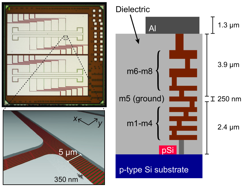
Devices were fabricated on mm2 die (Fig. 1) on a shared, 300-mm, multi-project wafer produced in a 90-nm CMOS process operated by IBM (9LP process designation). This process is primarily utilized for dense, high-performance digital circuits, and the trap die was one of many designs fabricated in parallel on the same wafer. The process allows for patterning of 8 copper interconnect layers, along with the top aluminum pad layer (right panel of Fig. 1). This m thick pad layer was used for the trap electrodes, and a copper layer (m5) approximately 4 m below the aluminum layer’s bottom surface and 2 m above the silicon substrate was used to form a ground plane under the extent of one of the traps. Due to metal density constraints arising from chemical-mechanical polishing steps applied to these layers, this ground plane was patterned as a mesh of 600 nm strips separated by 350 nm along the direction and 10 m along the direction (see Fig. 1). Metal vias connect this copper ground plane to the center electrode of the trap through the upper metal layers m6–m8.

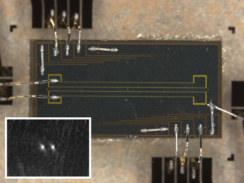
We designed and tested linear radio-frequency (RF) surface-electrodeChiaverini et al. (2005) Paul traps that confine ions 50 m from the electrode surface. The trap has a “five-wire” trap geometry, with two RF electrodes symmetric about the trap axis. Segmented dc control electrodes are routed to the corners of the trap chip to prevent wirebonds from obstructing laser access (see Fig. 2). This design offers flexibility to create various trapping potentials and allows scalability to multi-zone traps with complex geometries. Other advantages include comparative ease in selecting control voltages, and relatively narrow RF electrodes, allowing for lower capacitive coupling and RF power dissipation in the trap. Some inhomogeneity in RF field along the trap axis is anticipated due to the short (2 mm) electrode length, but effects on trapping are expected to be negligible.
A possible limitation to the use of high-resolution CMOS processing is breakdown at large applied potentials, especially since typical ion trap voltage amplitudes are significantly higher than those used in CMOS electronics. However, for up to 200 V static bias applied, the leakage current was below 10 pA, and no sudden increase corresponding to a dielectric breakdown was observed. We performed these tests at room temperature (in a high-dielectric-strength fluid to prevent air breakdown), applying the potential between one of the RF electrodes and either the ground plane or one of the adjacent dc electrodes in both types of trap.
After commercial foundry fabrication, trap chips (diced from the full die) approximately mm2 were bonded to a larger interposer to interface with the cold stage and wiring of a cryogenic vacuum system that allows for variation of the trap-chip temperatureSage, Kerman, and Chiaverini (2012). Using a quarter-wave helical resonator, a MHz RF signal of approximately 100 V amplitude was applied to the trap electrodes to produce radial trap frequencies of approximately – MHz, and an axial potential with frequencies near 1 MHz was produced by application of dc potentials of up to approximately 30 V to the segmented control electrodes. We load 88Sr+ ions by accelerating precooled Sr atoms from a magneto-optical trap toward the ion trap where they are photo-ionized and Doppler cooledSage, Kerman, and Chiaverini (2012). Although not measured precisely in this work, loading efficiency into these traps is similar to more conventionally fabricated surface-electrode traps using the same loading method.
Traps without a ground plane displayed significant laser-induced photo-effects due to the excitation of carriers in the silicon by scattered light used for atom photoionization (PI, 405 nm) and ion Doppler cooling (422 nm). During trap loading, this manifested itself as variation of the RF voltage amplitude on the trap electrodes due to varying impedance of the trap when the 405-nm PI light was on. The effects on the trapping potential were visible as ion motion synchronized to the PI light switch state. We observed no photo-effects in traps with a ground plane. Traps without a ground plane also exhibit strong trap-temperature-dependent nonlinearities in the resonance response of the voltage-step-up resonator. A ground plane reduces RF leakage into the silicon substrate sufficiently to eliminate this effect, such that we observed stable trapping for chip temperatures from 300 K down to 8 K. We noticed slightly more power dissipation in the foundry traps than in traps fabricated from gold or niobium on sapphire for similar RF voltage amplitudeChiaverini and Sage (2014), most likely due to higher dissipation in the metals or dielectrics. Ion lifetimes of more than an hour were observed in the presence of Doppler cooling light, equivalent to the best lifetimes seen in other traps measured in this vacuum system.
Excess micromotion (ion motion at the RF drive frequency) is caused by static electric fields that displace the ion from the RF null and can lead to ion heating. We compensate for this micromotion using the standard method of applying an additional opposing static field. Typical stray field values are on the order of 500 V/m here and appear stable over days. Although silicon oxide dielectric is exposed at the locations of gaps in the electrodes and may charge due to laser-induced photo-electron production, the stray field’s stability suggests another cause. Wirebonds, which are asymmetric with respect to the ion location and also closer to the ion here than in the case of larger trap chips, may be responsible for the steady stray electric field. The use of through-silicon-via technology can eliminate wirebonds from the chip surface, as has recently been demonstrated for surface-electrode ion trapsGuise et al. (2014).
When compared to single-metal-layer traps (SMLTs) on sapphire substrates, these traps exhibit increased scatter of laser light, possibly due to higher as-deposited roughness of the aluminum layer. We examined the trap-electrode surface using atomic force microscopy and measured an RMS roughness of 35 nm, significantly larger than the 2 nm we have measured on SMLTs. Scatter from the surface can be reduced by focusing laser beams to a smaller diameter at the trap.

Trapped-ion multi-qubit quantum operations can be limited by electric field noise that heats the ions’ shared vibrational modes in the trap, reducing gate fidelityWineland et al. (1998); Warring et al. (2013). Anomalously large heating rates caused by unknown noise sources have been seen in every trapped-ion experiment that has examined motional-state heating. This is particularly noticeable in small microfabricated traps as the heating rate appears to scale as for an ion a distance from a trap electrode surface. It is therefore important to characterize the heating rate in potentially scalable trap technologies.
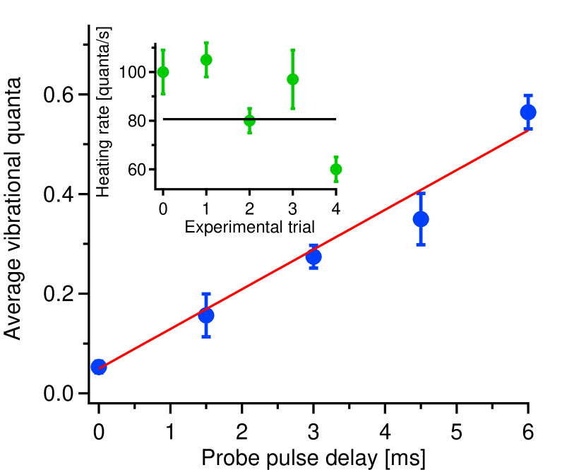
Using the dipole-forbidden transition in 88Sr+, we performed resolved-sideband cooling to prepare the ion in the ground state (average occupation ) of the 1.3 MHz axial vibrational mode and then measured the heating rate using sideband amplitude spectroscopy on this transition after a varying delayChiaverini and Sage (2014). Results of one such measurement are presented in Fig. 3 for a chip temperature of 8.4 K. Five measurements were recorded over a few days for nominally the same conditions; the average heating rate is 81(9) quanta/s. When scaled by to compare traps of different sizes, this heating rate is lower than that reported in any other trap fabricated on a silicon substrateBritton (2008); Leibrandt et al. (2009); Allcock et al. (2012); Wilpers et al. (2012); Vittorini et al. (2013); Niedermayr et al. (2014). Motional heating at this level would lead to an error of less than in a 100 s two-ion-qubit gate, below the fault-tolerance threshold for large scale quantum computing with surface-code error-correction schemesFowler, Stephens, and Groszkowski (2009).
We have shown basic functionality for quantum processing using a fabrication process, without modification, that has enabled scaling to billions of transistors. This is the first demonstration, in any physical implementation, of quantum computing hardware co-fabricated with scalable classical computing hardware. The fabrication of advanced CMOS and photonic technology on the trap chip, including the extensive existing libraries of integrated circuits for digital logic and memory, offers a straightforward path to scalable, local optical and electronic control and readout of trapped-ion arrays. The demonstration of stable trapping and low electric-field noise in a foundry-process trap is therefore an initial step toward integration of the required classical computing and photonic devices for useful, large-scale quantum processing with trapped ions.
Acknowledgements.
We thank Peter Murphy, Chris Thoummaraj, and Karen Magoon for assistance with ion-trap-chip packaging at Lincoln Laboratory. K.K.M. and R.J.R acknowledge funding from DARPA MTO, NSF iQuISE, and a DOE Science Graduate Fellowship. I.L.C. acknowledges funding from IARPA. The work at Lincoln Laboratory is sponsored by the Assistant Secretary of Defense for Research & Engineering under Air Force contract number FA8721-05-C-0002. Opinions, interpretations, conclusions, and recommendations are those of the authors and are not necessarily endorsed by the United States Government.References
- Leibfried et al. (2003) D. Leibfried, R. Blatt, C. Monroe, and D. Wineland, Rev. Mod. Phys. 75, 281 (2003).
- Blatt and Wineland (2008) R. Blatt and D. Wineland, Nature 453, 1008 (2008).
- Benhelm et al. (2008) J. Benhelm, G. Kirchmair, C. F. Roos, and R. Blatt, Nature Phys. 4, 463 (2008).
- Myerson et al. (2008) A. H. Myerson, D. J. Szwer, S. C. Webster, D. T. C. Allcock, M. J. Curtis, G. Imreh, J. A. Sherman, D. N. Stacey, A. M. Steane, and D. M. Lucas, Phys. Rev. Lett. 100, 200502 (2008).
- Brown et al. (2011) K. R. Brown, A. C. Wilson, Y. Colombe, C. Ospelkaus, A. M. Meier, E. Knill, D. Leibfried, and D. J. Wineland, Phys. Rev. A 84, 030303 (2011).
- Seidelin et al. (2006) S. Seidelin, J. Chiaverini, R. Reichle, J. J. Bollinger, D. Leibfried, J. Britton, J. H. Wesenberg, R. B. Blakestad, R. J. Epstein, D. B. Hume, W. M. Itano, J. D. Jost, C. Langer, R. Ozeri, N. Shiga, and D. J. Wineland, Phys. Rev. Lett. 96, 253003 (2006).
- Labaziewicz et al. (2008) J. Labaziewicz, Y. Ge, P. Antohi, D. Leibrandt, K. R. Brown, and I. L. Chuang, Phys. Rev. Lett. 100, 013001 (2008).
- Britton (2008) J. Britton, Microfabrication techniques for trapped ion quantum information processing, PhD dissertation, University of Colorado (2008), arXiv:1008.2222 .
- Leibrandt et al. (2009) D. Leibrandt, J. Labaziewicz, R. Clark, I. Chuang, R. Epstein, C. Ospelkaus, J. Wesenberg, J. Bollinger, D. Leibfried, D. Wineland, D. Stick, J. Sterk, C. Monroe, C.-S. Pai, Y. Low, R. Frahm, and R. Slusher, Quant. Inf. Comp. 9, 0901 (2009).
- Stick et al. (2010) D. Stick, K. M. Fortier, R. Haltli, C. Highstrete, D. L. Moehring, C. Tigges, and M. G. Blain, (2010), arXiv:1008.0990v2 .
- Allcock et al. (2012) D. Allcock, T. Harty, H. Janacek, N. Linke, C. Ballance, A. Steane, D. Lucas, R. Jarecki, S. Habermehl, M. Blain, D. Stick, and D. Moehring, Appl. Phys. B 107, 913 (2012).
- Wilpers et al. (2012) G. Wilpers, P. See, P. Gill, and A. G. Sinclair, Nature Nanotechnology 7, 572 (2012).
- Wright et al. (2013) K. Wright, J. M. Amini, D. L. Faircloth, C. Volin, S. C. Doret, H. Hayden, C.-S. Pai, D. W. Landgren, D. Denison, T. Killian, R. E. Slusher, and A. W. Harter, New Journal of Physics 15, 033004 (2013).
- Niedermayr et al. (2014) M. Niedermayr, K. Lakhmanskiy, M. Kumph, S. Partel, J. Edlinger, M. Brownnutt, and R. Blatt, (2014), arXiv:1403.5208 .
- Sterling et al. (2014) R. C. Sterling, H. Rattanasonti, S. Weidt, K. Lake, P. Srinivasan, S. C. Webster, M. Kraft, and W. K. Hensinger, Nature Communications 5, (2014).
- Field et al. (2010) R. M. Field, J. Lary, J. Cohn, L. Paninski, and K. L. Shepard, Applied Physics Letters 97, 211111 (2010).
- Orcutt et al. (2012) J. S. Orcutt, B. Moss, C. Sun, J. Leu, M. Georgas, J. Shainline, E. Zgraggen, H. Li, J. Sun, M. Weaver, S. Urošević, M. Popović, R. J. Ram, and V. Stojanović, Opt. Express 20, 12222 (2012).
- Chiaverini et al. (2005) J. Chiaverini, R. B. Blakestad, J. Britton, J. D. Jost, C. Langer, D. Leibfried, R. Ozeri, and D. J. Wineland, Quant. Inf. Comp. 5, 419 (2005).
- Sage, Kerman, and Chiaverini (2012) J. M. Sage, A. J. Kerman, and J. Chiaverini, Phys. Rev. A 86, 013417 (2012).
- Chiaverini and Sage (2014) J. Chiaverini and J. M. Sage, Phys. Rev. A 89, 012318 (2014).
- Guise et al. (2014) N. D. Guise, S. D. Fallek, H. Hayden, C.-S. Pai, C. Volin, K. R. Brown, J. T. Merrill, A. W. Harter, J. M. Amini, L. M. Lust, K. Muldoon, D. Carlson, and J. Budach, Review of Scientific Instruments 85, 063101 (2014), arXiv:1403.3662 .
- Wineland et al. (1998) D. Wineland, C. Monroe, W. M. Itano, D. Leibfried, B. E. King, and D. M. Meekhof, J. Res. Natl Inst. Stand. Technol. 103, 259 (1998).
- Warring et al. (2013) U. Warring, C. Ospelkaus, Y. Colombe, K. R. Brown, J. M. Amini, M. Carsjens, D. Leibfried, and D. J. Wineland, Phys. Rev. A 87, 013437 (2013).
- Vittorini et al. (2013) G. Vittorini, K. Wright, K. R. Brown, A. W. Harter, and S. C. Doret, Review of Scientific Instruments 84, 043112 (2013).
- Fowler, Stephens, and Groszkowski (2009) A. G. Fowler, A. M. Stephens, and P. Groszkowski, Phys. Rev. A 80, 052312 (2009).