Electrochemical doping of few layer ZrNCl from first-principles:
electronic and structural properties in field-effect configuration
Abstract
We develop a first-principles theoretical approach to doping in field-effect devices. The method allows for calculation of the electronic structure as well as complete structural relaxation in field-effect configuration using density-functional theory. We apply our approach to ionic-liquid-based field-effect doping of monolayer, bilayer, and trilayer ZrNCl and analyze in detail the structural changes induced by the electric field. We show that, contrary to what is assumed in previous experimental works, only one ZrNCl layer is electrochemically doped and that this induces large structural changes within the layer. Surprisingly, despite these structural and electronic changes, the density of states at the Fermi energy is independent of the doping. Our findings imply a substantial revision of the phase diagram of electrochemically doped ZrNCl and elucidate crucial differences with superconductivity in Li intercalated bulk ZrNCl.
pacs:
73.22.-f, 71.15.MbI Introduction
In recent years, materials with reduced dimensionality have attracted a lot of attention because of their interesting physical properties and proposed applications range from electronics to sensing. In addition to graphene, which is probably the most studied two-dimensional (2D) material, monolayers or few-layer systems (nanolayers) of layered materials such as transition metal dichalcogenidesRadisavljevic et al. (2011); Ye et al. (2012); Yuan et al. (2013); Radisavljevic and Kis (2013); Wu et al. (2013); Das et al. (2013); Das and Appenzeller (2013) or chloronitridesYe et al. (2010); Kasahara et al. (2010); Schurz et al. (2011); Zhang et al. (2012a); Ekino et al. (2013) are gaining importance because of their intrinsic band gap. The possibility of doping these few layer systems with field-effect transistors (FETs) is particularly appealing. In ionic-liquid-based FETs the charging of the nanolayers is substantial and thus allows for electrochemical doping of few-layer materialsYuan et al. (2009); Ye et al. (2010, 2012); Zhang et al. (2012b); Taniguchi et al. (2012); Yuan et al. (2013); Perera et al. (2013) with surface charges of the order of . In the field of condensed matter physics, this prospect is very appealing as it becomes possible to dope ultrathin films of layered material and explore their phase diagram to detect charge-density waves, spin-density waves, or superconducting instabilities in reduced dimensionality. Furthermore, it was recently shown that the device characteristics of FETs using an ionic-liquid are much better than those of back-gated devicesPerera et al. (2013).
An eminent example is the electrochemical doping of the semiconducting chloronitride ZrNClYe et al. (2010). It has been shown by Ye et al. that ZrNCl flakes can be made first metallic and then superconducting by electrochemical doping. A similar behavior has also been detected in MoS2 flakesYe et al. (2012). Despite these challenging experimental perspectives, the understanding of electronic and structural properties at high electric field in FET configuration is still limited. For example, the effects of the large electric field (in the order of Ye et al. (2010, 2012)) on the structural properties of the nanolayer remains an open question. Moreover, in the case of ZrNCl, the surface charge, and consequently the effective doping, changes by an order of magnitude depending on the assumed thickness of the charge layerYe et al. (2010). It is then crucial to address these issues to determine the phase diagram of electrochemically doped ZrNCl.
We develop a first-principles theoretical approach to doping in field-effect devices. The method allows for calculation of the electronic structure as well as complete structural relaxation in field-effect configuration using density-functional theory. We apply our approach to ionic-liquid-based field-effect doping of monolayer, bilayer, and trilayer ZrNCl.
The paper is organized as follows: in Sec. II we give a brief introduction to field-effect doping and a description of the model we use in order to investigate such systems from first-principles, along with the computational details. Results for the specific example of the electrochemical doping of ZrNCl are presented in Sec. III. First, we show the structural changes in field-effect configuration and then investigate the distribution of the induced charge in more detail. Afterwards we use a simple model to describe the modification of the band structure and show that, despite the structural and electronic changes, the density of states at the Fermi energy is independent of the doping. Finally, conclusions are presented in Sec. IV.
II Theoretical background
II.1 Field-effect configuration
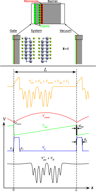
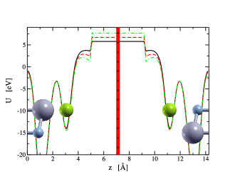
In Fig. 1 the typical setup for a field-effect measurement is shown. The system is separated from the gate electrode by a dielectric such as silicon oxide. Applying a gate voltage between the system and the gate results in a change in the Fermi level of the metal () with respect to the one in the system (). Hence, the dielectric is polarized due to the opposite charges at the dielectric/metal and dielectric/system interfaces.

The distribution of charges in the system/dielectric/ metal-gate system generates the potential profile shown in Fig. 1. Inside the dielectric, a constant and finite electric field (linear potential) occurs due only to the opposite signs of the charges on the different sides of the dielectric. At the system/dielectric interface (on the system side), the potential varies very quickly because of the strongly inhomogeneous charge distribution in the first few layers of the system. Finally, inside the system and far from the dielectric, the potential felt by the electrons oscillates with a periodicity that is related to the crystal periodicity and is determined by the ionic positions. In this region, the spatial average of the electric field is zero. The same situation occurs inside the metal gate far from the dielectric.
In order to describe such a setup in theory, different methods have been used in the past. In perhaps the most advanced method one takes into account the connection of the system to the gate electrode and the back contact, effectively simulating an open-boundary system. This can be achieved by coupling the calculation of the electronic structure of the system—often done within density-functional theory (DFT)—with the Keldysh nonequilibrium Green’s function (NEGF) formalismLiu et al. (2012); Gong et al. (2013). However, these calculations are very expensive since the electrostatic potential of the system has to be determined self-consistently. This is achieved by solving the Poisson equation with the bulk-like Hartree potentials of the electrodes as boundary conditions on the interfaces between the electrodes and the system. In fact, by using NEGF, one is often restricted to use the structure which was relaxed without electric field, effectively neglecting the interplay of electric field, charging, electronic structure, and the geometry of the systemLiu et al. (2012); Gong et al. (2013). Furthermore, these simulations of the full system/dielectric/metal-gate system are not only difficult and time consuming but also unnecessary, as we are mainly interested in what happens at the system/dielectric interface. We thus need to simplify the modeling of the FET measurements.
The first simplification is to include the external electric field and eliminate the metallic gate. This amounts to replacing the metallic gate with a charged plate that simulates the charge occurring on the gated metal surface in contact with the dielectricGava et al. (2009); Uchida and Okada (2009). It is important to remark that, if the charged plate is neglected and only an external field is added, no charging can occur on the system side.
After eliminating the gate, the next step is trying to reduce the size of the dielectric or to eliminate it completely. Since we expect that the relevant physics occurs inside the system in close contact with the dielectric, it is possible to replace the several nanometer thick-dielectric with a much thinner one. This is not an approximation, but is what is found in modern nanoelectronics, where, in order to increase the FET capacity, thinner and thinner dielectrics are used. Finally, the ultimate approximation is the complete removal of the dielectric, and including the charged plate close to the position of the system/dielectric interface.
The total removal of the dielectric can be achieved by following the steps mentioned above, as long as the ions of the system are fixed. However, we also want to simulate the structural relaxation of the system in FET configuration, which means that we need to allow the ions to move. In this case an additional problem occurs. Having totally eliminated the dielectric, the ions can move too close to the charged plate which simulates the gate electrode (opposite charge on the plate and the system). This can be avoided by representing the dielectric with a constant potential barrier which effectively mimics the physical repulsion exerted by the dielectric. This is the approximation adopted in the present work.
Up to now, we have introduced a simpler model of the system/dielectric/gate system that works with open boundary conditions. An additional conceptual step is needed in order to simulate the FET using periodic boundary conditions (PBC). With PBC, the charged plate interacts with the periodic image of the system generating a spurious electric field. This is unphysical, as in experiments far from the dielectric and inside the system or the metal gate the average electric field must be zero. One way to circumvent this issue is to include a mirror image of the system that forces the electric field to be zero between the periodic imagesUchida and Okada (2009). However this implies calculating a system with twice the number of atoms and results in an higher computational load. A smarter solution comes from electrostatics. It is indeed sufficient to add an additional dipole plate (two planes of opposite chargeBengtsson (1999)) generating an electric field that exactly cancels the one on the left side of the gate in Fig. 1. In this case no additional computational load is needed and the condition of zero electric field far from the system/dielectric interface is enforced.
II.2 Model
The general setup we use to model a system in FET configuration using PBC in the three spatial directions is shown in Fig. 2. The nanolayers are placed in front of a charged planeGava et al. (2009); Uchida and Okada (2009) which models the gate as already mentioned in the last section (henceforth referred to as “monopole”). The layers are then charged with the same amount of opposite charge ( and are the number of doped electrons per unit area and the area of the unit cell parallel to the surface respectively) which will lead to a finite electric field in the region between the gate and the system. In the vacuum region between the repeated images (PBC) the electric field has to be zero in order to correctly determine the changes in the electronic structure and the geometry for such a field effect setup. However, the dipole of the charged system and the gate leads to an artificial electric field between the different slabs of the repeated unit cell since in PBC the electric field averaged over the unit cell is zero. We thus include an electric dipole generated by two planes of opposite chargeNeugebauer and Scheffler (1992); Bengtsson (1999); Meyer and Vanderbilt (2001) which are in the vacuum region next to the monopole (Fig. 2). We furthermore include a potential barrier to avoid the direct interaction between the charge density of the system and the monopole/dipole. The resulting total potential together with the definition of the different variables used in the following discussion is shown in Fig. 2.
The total energy of the system in this model-FET setup is given as
| (1) |
The first term appearing on the right-hand side of Eq. (1) is the total energy calculated within PBC using the periodic, bare ion-electron potential
| (2) |
Here the first four terms represent the kinetic energy, Hartree energy, exchange-correlation energy, and Madelung energy, respectively, while the last term is the bare ion-electron energy with being the electron density. is the energy associated with the monopole while is the energy due to the dipole. The interaction with the potential barrier which is used to mimic the dielectric is given by the last term in Eq. (1), .
The total charge density in the cell is the sum of the electronic part, the ionic part, and the monopole charge
| (3) |
where , , and are the electron, ion, and monopole charge densities, respectively. Furthermore, is the (pseudo) atomic charge of atom at position , and the monopole with a total charge of per unit cell is located at . Within PBC, the interaction energy associated to the presence of the monopole is given by
| (4) |
where can be written as
| (5) |
Here with measures the distance to the monopole which is at and is the length of the periodically repeated unit cell along (see Fig. 2). Notice that represents the potential generated in PBC by the monopole plane of total charge placed at (the linear term) and by a uniform jellium density of opposite total charge (the quadratic term). This jellium charge cancels the uniform background charge which is used in standard plane-wave ab initio codes in order to have a neutral systemGava et al. (2009). The last term in Eq. (5) is constant and it is conventionally chosen in order to have .
To eliminate the electrostatic interactions between repeated cells in the direction, we introduce a dipole formed by two opposite-charged planes at and . The dipole should be placed between the monopole and the vacuum. This condition is realized by choosing , where is a small positive number. In order to calculate the dipole energy we need to determine the electric dipole moment per unit surface of the full system (i.e., using the sum of ionic, electronic, and monopole charge density)Bengtsson (1999); Meyer and Vanderbilt (2001)
| (6) |
Here is a periodic function having different definitions for values of that are inbetween the two charged planes of the dipole or elsewhere, namely:
| (7) |
with , (and periodically repeated). The dipole energy is given bynot
| (8) |
while the potential generated by the two planes of opposite charge can be written as
| (9) |
Note that in a self-consistent calculation the charge density changes with each iteration. Thus, the dipole moment per unit surface and the corresponding potential which represents the dipole have to be recalculated on each iteration until self-consistency is achieved.
Finally, we place a barrier, mimicking the repulsion by the dielectric, to separate the system from the monopole plane. Such barrier, of height and thickness , starts at , in correspondence of the first plane of the dipole, and ends at . The associated energy is
| (10) |
where is a periodic function of defined on the interval as
| (11) |
In the present implementation, we have chosen a linear transition from to within in order to minimize the fluctuation of the potential in space.
The final, full Kohn-Sham potential of the gated system can be written as
| (12) |
where is the bare, periodic electron-ion potential, is the normal Hartree potential
| (13) |
is the exchange-correlation potential, and , , , are the monopole, dipole, and potential barrier, given in Eqs. (5), (9), and (11), respectively. The different parts of the Kohn-Sham potential are also shown in Fig. 2.
For the structural optimization we need to calculate the total force on atom . Using the Hellman-Feynman theorem and Eq. (1) the force can be written as111Notice that if the barrier potential is correctly chosen, the nuclei never enter the barrier region and the last term of Eq.(II.2) is always equal to zero. The repulsive force on the system is mediated by the tail of the electron distribution within the barrier region. Such repulsion is included in the terms of Eq.(II.2) which implicitly or explicitly depend on the electron charge density .
| (14) |
Using this equation we can now relax the system in an FET setup. We explicitly verified the force calculation by finite differences.
II.3 Computational details
All calculations were performed using DFT with a modified version of the PWscf code of the Quantum ESPRESSO packageGiannozzi et al. (2009). We used the Perdew-Zunger local density approximation (LDA) exchange-correlation functionalPerdew and Zunger (1981) together with ultrasoft pseudopotentials including core corrections. We cross-checked our results with the Perdew-Burke-Ernzerhof (PBE) functionalPerdew et al. (1996) including dispersion correctionsGrimme (2006) (“+D2”). A plane-wave basis set was used to describe the valence electron wave function and density up to a kinetic energy cutoff of and (), respectively. The electronic eigenstates have been occupied with a Fermi-Dirac distribution, using an electronic temperature of . The BZ integration has been performed with a Monkhorst-Pack gridMonkhorst and Pack (1976) of for the charged systems and points for the neutral one. In order to correctly determine the Fermi energy in the charged system, we performed a non-self-consistent calculation on a denser -point grid of points starting from the converged charge density. The self-consistent solution of the Kohn-Sham equations was obtained when the total energy changed by less than and the maximum force on all atoms was less than ( is the Bohr radius). A tight force convergence threshold was necessary since the force on the atoms due to the charged plane representing the gate can be as small as for the lighter nitrogen atoms.
Using the experimental lattice parameters of bulk -ZrNCl as starting geometryShamoto et al. (1998), we relaxed the unit cell for the bulk system until the total stress on the system was less than . The lattice parameters thus determined agree well with the experimental values: for the in-plane lattice constant we found a value of (Exp.: ) and for the perpendicular constant we calculated (Exp.: ). The deviation of about 1% is in the range of variations typically found for LDA calculations. Using PBE+D2 the deviations can be decreased to less than 1%, but the convergence for the layered-2D systems is slower, especially if ZrNCl is close to the position of the monopole potential. Since we are mainly interested in the general behavior of the system under the influence of a gate voltage we continue to use the LDA. We cross-checked our results for selected gate voltages using PBE+D2 and got the same general behavior with only small changes. The final geometry of the bulk system was used as the starting geometry for the calculations of the layered-2D systems fixing the size of the unit cell in plane and increasing the perpendicular size such that the vacuum region between the repeated images was at least . We investigated single-, double-, and triple-layer systems with different doping levels ranging from to electrons per unit cell (i.e., to electrons per Zr atom since we are using the hexagonal unit cell) which corresponds to a doping charge per unit surface ranging from to .
The dipole was placed at with and for single- and double-layer ZrNCl, and in the trilayer case. A potential barrier with an height of and a width of was used in order to prevent the ions from moving too close to the monopole. The final results were found to be independent of the separation of the dipole planes, as well as the barrier height and width as long as it is high or thick enough to ensure that .
III Results
III.1 Structural changes under electrochemical doping
In the relevant experiment of Ref. 8 on ZrNCl an ionic liquid was used as dielectric and the gate voltage was applied between the ionic liquid and ZrNCl. The mobile cation and anion of the ionic liquid move towards the oppositely charged electrode which in turn leads to the formation of an electric double layer (EDL) at the interface to ZrNCl. The EDL at the ZrNCl/ionic liquid interface acts as a capacitor with a huge capacitance (“supercapacitor”) and can accumulate charges in the transport channel between source and drain. Using such an electric double-layer transistor one can achieve large carrier densities up to (see Ref. 13) thus allowing the investigation of the transition from a band insulator to a metal and, eventually, to a superconductorYe et al. (2010).
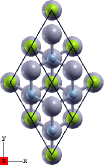
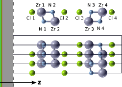
The thickness of the EDL is mainly determined by the size of the ions, the microscopic structure of the surface, and the interaction between both. In this work we simulate the gate with the monopole potential (Eq. (5)) as shown in Fig. 2, which has a fixed position . We thus need to relax the nanolayers towards the charged plane of the monopole potential until the attractive force between the two oppositely charged systems is compensated by the repulsive force due to the electron density within the potential barrier, . In this section we analyze the final geometry with increasing doping (i.e., increasing strength of the monopole potential) in detail. Figure 3 shows the atomic structure of a double-layer ZrNCl together with the definition of the atoms which are used in the following discussion and their position with respect to the interface between system and ionic liquid.
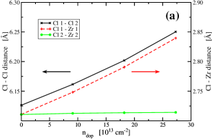
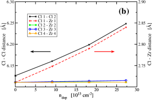
The bonding between the neutral layers of ZrNCl is very weakHeid and Bohnen (2005); Akashi et al. (2012) which allows for the intercalation with alkaline elements or even moleculesKasahara et al. (2010). Thus, the interaction between ZrNCl and the monopole potential representing the gate could in principle strongly change the interlayer distance depending on the distribution of the doping charge. In our calculations however, we find that the interlayer distance is nearly unchanged. Instead the thickness of the nanolayers system is increased, due mainly to the change in the Cl-Zr distance for the chlorine closest to the gate, while the other distances are nearly constant as can be seen in Fig. 4.
The interlayer distance in the bilayer case changes by less than 1% compared to the value of bulk ZrNCl. Triple-layer ZrNCl shows the same general behavior—we find an increase of about 1% in the distance between the middle layer and the one next to the charged plane from for to for (bulk value ). The absolute value of these interlayer distances, in principle, depends on the correct description of the van der Waals interactions between the layers and, thus, might be questionable. The most important result is that for all investigated systems the major changes in the geometry occur in the layer next to the monopole (see Fig. 3).
This is also the case for the different Zr-N bond lengths, and angles of the Zr-N rhomboid. In the double- and triple-layer system relevant changes occur only in the layer next to the monopole. As the relaxed geometry of the ZrNCl layer closer to the monopole are very similar for the single-, double-, and triple-layer case, we only present the results of the structural minimization of a single layer (see Fig. 5).
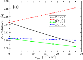
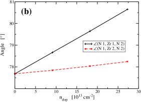
Due to the large difference between the electronegativity of nitrogen and zirconium, the nitrogen is partially negative. Accordingly, N is attracted by the positively charged plane representing the gate. This leads to an increase of the bond length labeled “Zr 2 - N 1” which is the bond with the nitrogen closer to the monopole as can be seen in Fig. 5(a). On the other hand, the bond length in which the zirconium is closer to the monopole is decreased (“Zr 1 - N 2”). Since the in-plane bonds are nearly unchanged the N-Zr-N angles are modified considerably as can be seen in Fig. 5(b). These changes in the geometry of the layer next to the monopole are due to the fact that the doping charge is mainly localized within this layer as we will see in the next section.
III.2 Electronic structure
As shown in the last section, the structure of the layer closest to the monopole is strongly affected by the electric field. This is due to the interplay between the electric field, the doping charge, and the specific band structure of ZrNCl. The conduction band minimum is located at the and pointAkashi et al. (2012); Sugimoto and Oguchi (2004); Heid and Bohnen (2005) and has a nearly quadratic in-plane dispersion . Furthermore, the band consists mainly of Zr -states which together with the weak interlayer interaction leads to a negligible dispersion along . Thus, it can be expected that the doping charge is mainly localized within the center of the layers closest to the ionic liquid.
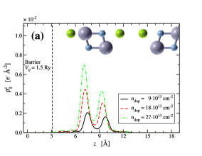
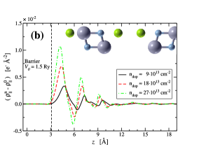
Figure 6(a) shows the distribution of the conduction band electrons in bilayer ZrNCl averaged over the directions parallel to the layers for three doping levels ranging from to . The doping charge occupying the conduction band is mainly localized in the center of the layer closest to the monopole and has a strong asymmetry between the two Zr-N planes on either side. This asymmetry is due to the electric field and the induced structural changes. The field induce not only an asymmetry in the geometry and the distribution of the conduction band electrons but also an increased surface dipole . In Fig. 6(b) the difference between the full charge density of the doped system and the undoped system is shown, where was calculated with the relaxed geometry of the charged one. This charge difference represents the screening charge of the gate electric field, including both the metallic screening of the conduction band and the dielectric screening of the lower, occupied valence bands which rearrange under the applied electric field. The field has two main effects as can be seen in Fig. 6: firstly, it leads to an asymmetry in the charge distribution and consequently in the geometry as discussed in the last section, and secondly, it increases the surface dipole—not only due to the structural changes but also due to the rearrangement of the charge density of the undoped system . In fact, the induced dipole is largest close to the last chlorine (Fig. 6(b)), even if the doping charge in the conduction band is localized within the center of the layer (Fig. 6(a)).
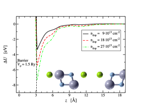
The strong localization of the doping charge within the first layer also leads to a complete screening of the electric field. Figure 7 shows the difference of the planar averaged potential of the charged and the uncharged system , the derivative of which being proportional to the effective electric field . The slope of the potential close to the potential barrier at increases with increasing doping and the total potential changes mainly within the layer of ZrNCl which is closer to the monopole. The largest change and, thus, the largest electric field can be found close to the outermost chlorine atom.
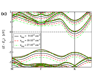
The band structure for different number of layers is shown in Fig. 8. Since the doping charge is localized within the layer close to the ionic liquid/system interface, only the electronic structure of this layer is influenced and, accordingly, the degeneracy of the conduction band at the and point is lifted. The bands localized on the doped layer are shifted down in energy while those of the undoped layers are unchanged as can be seen in Figs. 8(b) and (c) for bilayer and trilayer ZrNCl, respectively. Also the former valence band is nearly unchanged despite the geometrical changes (cf., Figs. 4 and 5).
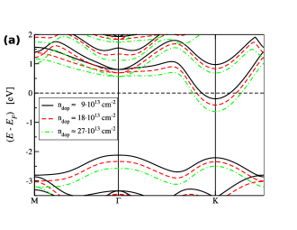
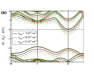
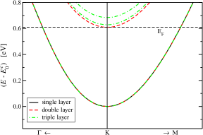
Aligning the band structure for different number of layers to the minimum of the conduction band as in Fig. 9 demonstrates again that there is effectively no difference between the monolayer/bilayer/trilayer systems. Thus, in this section we focus in the following on the single-layer system and analyze the variations of the partially occupied band on doping in more detail.
Charging of the monolayer does not simply act as a rigid doping as it also affects the shape of the band. In order to describe the changes in the band structure quantitatively we model the dispersion relation near the and points by a 4th order Taylor expansion in , compatible with the symmetry of the bands:
| (15) |
Here is aligned with the direction and measures the distance from the , special points. The term is needed to describe the trigonal warping of the conduction band while both the 3rd the 4th order term are necessary to allow for the deviations of the density of states from the constant energy dependence of a perfect 2D electron gas. The parameters , , and obtained by fitting Eq. (III.2) to the band structure of single-layer ZrNCl for three different doping levels are depicted in Fig. 10. Most interestingly, the effective mass changes by 20% in the doping regime investigated here, which would lead to the same change in the density of states (DOS) for a perfect 2D electron gas which can be modeled using just the first two terms in Eq. (III.2).
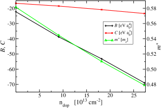
Yet the parameters and , which describe the deviations from a quadratic dispersion for higher values of , change considerably when the doping is increased. The decrease from about to for and from about to for compensate the change in the effective mass . Accordingly the DOS at the Fermi energy stays more or less constant as can be seen in Fig. 11.
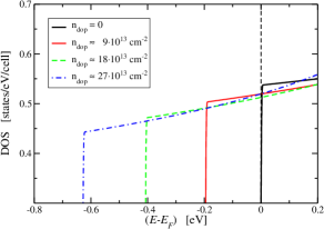
In fact, specific heat measurements on Li intercalated ZrNCl suggested that the DOS at the Fermi energy is not increased with increasing dopingKasahara et al. (2009), which cannot be explained assuming a rigid doping since the DOS is not flat (cf., Refs. 35; 33; 34 and Fig. 11).
In our simulated electric double-layer transistor (EDLT) the DOS at the Fermi energy is constant since the band structure is changed upon doping. However, does this picture hold for bulk LixZrNCl? As a first attempt to simulate the Li intercalation in the bulk system with our model, we substitute the Lix plane in bulk LixZrNCl (i.e., periodic in all three dimension) with a charged plane as described in Eq. (5)—a sketch of the model is shown in Fig. 12.
Similarly to the EDLT setup we find a decreasing effective mass even if the decrease is smaller as can be seen as green (light gray) line in Fig. 13(a) labeled “symmetric”. Since a rigid structure in field-effect configuration also shows this behavior (red (grey) curve in Fig. 13(a) labeled “EDLT without relaxation”), it can neither be related to the EDLT setup nor to the field-induced structural changes. Instead, it might be a system-specific property.

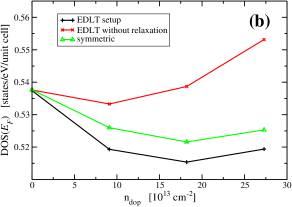
However, the decreasing effective mass is again compensated by the change in the parameters and as can be seen in Fig. 13(b). Further increasing the doping would ultimately lead to an increasing DOS at the Fermi energy for all investigated systems. Finally, we also note that the maximum possible doping is smaller if the nanolayer system is not relaxed in the presence of the electric field generated by the potential in Eq. (5). This shows again the importance of the structural relaxation for the correct theoretical description of ZrNCl in an FET setup.
IV Implications for superconductivity
Electrochemical doping of ZrNCl is appealing as an insulator-superconductor transition occurs as a function of chargingYe et al. (2010), as shown in Fig. 14. The critical doping of the insulator-superconductor transition and the behavior of the superconducting critical temperature as a function of doping depends crucially on the depth of the induced charge layer in the sample. Indeed, if the induced charge layer is deeper, then for a given gate voltage the charge density per layer (and thus the doping) is smaller. Thus knowledge of the charge distribution in the ZrNCl flakes is a crucial parameter to determine the phase diagram.
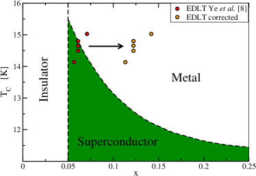
While the gate voltage and the total induced charge (Hall effect) are accessible quantities, the depth of the induced charge layer is not. Thus experimentalist are forced to use simplified screening models to access this quantity. In the case of electrochemically doped ZrNCl, Ye et al. in Ref. 8 assumed that the induced charge is localized on two ZrNCl layers. Under this assumption, they obtained the phase diagram in Fig. 14, showing a similar behavior for Li-intercalated and electrochemically doped ZrNCl. However, we have shown in the last section that this assumption is not well grounded, as the depth of the induced charge layer is only one ZrNCl layer, and not two. Furthermore we have shown that the charge distribution inside the outermost ZrNCl layer is strongly inhomogeneous. These findings imply a redrawing of the ZrNCl phase diagram, as shown in Fig. 14. In particular, in the revised phase diagram of electrochemically doped samples, superconductivity occurs at doping larger then and Tc increases monotonically from a minimum value of up to a maximum of at a doping of . This is in striking contrast with chemically intercalated bulk ZrNCl samples, in which superconductivity occurs at a doping of with T. Moreover, in the bulk case, Tc decreases monotonically as a function of doping, as show in Fig. 14. Thus, our work points out crucial differences in superconductivity in Li intercalated bulk ZrNCl. Further calculations for, e.g., the transition temperature are beyond the scope of this paper and will be addressed in a separate work.
V Conclusions
In this work we developed a first principles approach to field-effect doping. The method allows for the calculation of electronic structure and structural optimization under an applied electric field in an FET configuration. We have applied the method to the transition-metal chloronitride ZrNCl and have shown that the electric field induces substantial deformation of bond lengths and angles in the outermost ZrNCl layer in contact with the ionic liquid. The most evident deformation generated by the electric field is the large change of the the N-Zr-N angles. The electronic structure is also affected by the large electric field as the effective mass of the electron is substantially reduced as a function of increasing charge. The density of states at the Fermi level is, however, essentially independent on doping. Furthermore, we have shown that the depth of the induced charge layer is only one ZrNCl layer and that the charge distribution inside the outermost ZrNCl layer is strongly inhomogeneous. These findings imply a substantial revision of the phase diagram of electrochemically doped ZrNCl and elucidate crucial differences with superconductivity in Li intercalated bulk ZrNCl.
Acknowledgements.
The authors acknowledge financial support of the Graphene Flagship and of the French National ANR funds within the Investissements d’Avenir programme under reference ANR-11-IDEX-0004-02, ANR-11-BS04-0019 and ANR-13-IS10-0003-01. Computer facilities were provided by CINES, CCRT and IDRIS (project no. x2014091202).References
- Radisavljevic et al. (2011) B. Radisavljevic, A. Radenovic, J. Brivio, V. Giacometti, and A. Kis, Nat. Nano. 6, 147 (2011).
- Ye et al. (2012) J. T. Ye, Y. J. Zhang, R. Akashi, M. S. Bahramy, R. Arita, and Y. Iwasa, Science 338, 1193 (2012).
- Yuan et al. (2013) H. Yuan, M. S. Bahramy, K. Morimoto, S. Wu, K. Nomura, B.-J. Yang, H. Shimotani, R. Suzuki, M. Toh, C. Kloc, X. Xu, R. Arita, N. Nagaosa, and Y. Iwasa, Nat. Phys. 9, 563 (2013).
- Radisavljevic and Kis (2013) B. Radisavljevic and A. Kis, Nat. Mater. 12, 815 (2013).
- Wu et al. (2013) S. Wu, J. S. Ross, G.-B. Liu, G. Aivazian, A. Jones, Z. Fei, W. Zhu, D. Xiao, W. Yao, D. Cobden, and X. Xu, Nat. Phys. 9, 149 (2013).
- Das et al. (2013) S. Das, H.-Y. Chen, A. V. Penumatcha, and J. Appenzeller, Nano Lett. 13, 100 (2013).
- Das and Appenzeller (2013) S. Das and J. Appenzeller, Nano Lett. 13, 3396 (2013).
- Ye et al. (2010) J. T. Ye, S. Inoue, K. Kobayashi, Y. Kasahara, H. T. Yuan, H. Shimotani, and Y. Iwasa, Nat. Mater. 9, 125 (2010).
- Kasahara et al. (2010) Y. Kasahara, T. Kishiume, K. Kobayashi, Y. Taguchi, and Y. Iwasa, Phys. Rev. B 82, 054504 (2010).
- Schurz et al. (2011) C. M. Schurz, L. Shlyk, T. Schleid, and R. Niewa, Z. Kristallogr. 226, 395 (2011).
- Zhang et al. (2012a) S. Zhang, M. Tanaka, and S. Yamanaka, Phys. Rev. B 86, 024516 (2012a).
- Ekino et al. (2013) T. Ekino, A. Sugimoto, A. M. Gabovich, Z. Zheng, and S. Yamanaka, Physica C 494, 89 (2013).
- Yuan et al. (2009) H. Yuan, H. Shimotani, A. Tsukazaki, A. Ohtomo, M. Kawasaki, and Y. Iwasa, Adv. Funct. Mater. 19, 1046 (2009).
- Zhang et al. (2012b) Y. Zhang, J. Ye, Y. Matsuhashi, and Y. Iwasa, Nano Lett. 12, 1136 (2012b).
- Taniguchi et al. (2012) K. Taniguchi, A. Matsumoto, H. Shimotani, and H. Takagi, Appl. Phys. Lett. 101, 042603 (2012).
- Perera et al. (2013) M. M. Perera, M.-W. Lin, H.-J. Chuang, B. P. Chamlagain, C. Wang, X. Tan, M. M.-C. Cheng, D. Tománek, and Z. Zhou, ACS Nano 7, 4449 (2013).
- Liu et al. (2012) Q. Liu, L. Li, Y. Li, Z. Gao, Z. Chen, and J. Lu, J. Phys. Chem. C 116, 21556 (2012).
- Gong et al. (2013) K. Gong, L. Zhang, D. Liu, L. Liu, Y. Zhu, Y. Zhao, and H. Guo, “Electric control of spin in monolayer wse2 field effect transistors,” (2013), arXiv:1310.1816 .
- Gava et al. (2009) P. Gava, M. Lazzeri, A. M. Saitta, and F. Mauri, Phys. Rev. B 79, 165431 (2009).
- Uchida and Okada (2009) K. Uchida and S. Okada, Phys. Rev. B 79, 085402 (2009).
- Bengtsson (1999) L. Bengtsson, Phys. Rev. B 59, 12301 (1999).
- Neugebauer and Scheffler (1992) J. Neugebauer and M. Scheffler, Phys. Rev. B 46, 16067 (1992).
- Meyer and Vanderbilt (2001) B. Meyer and D. Vanderbilt, Phys. Rev. B 63, 205426 (2001).
- Topsakal and Ciraci (2012) M. Topsakal and S. Ciraci, Phys. Rev. B 85, 045121 (2012).
- (25) Note that we use a different notation than Lennart Bengtsson in Ref. 21. Following his notation results in changing his definition of the dipole correction energy (Eq. (13) of Ref. 21) to .
- Note (1) Notice that if the barrier potential is correctly chosen, the nuclei never enter the barrier region and the last term of Eq.(II.2) is always equal to zero. The repulsive force on the system is mediated by the tail of the electron distribution within the barrier region. Such repulsion is included in the terms of Eq.(II.2) which implicitly or explicitly depend on the electron charge density .
- Giannozzi et al. (2009) P. Giannozzi, S. Baroni, N. Bonini, M. Calandra, R. Car, C. Cavazzoni, D. Ceresoli, G. L. Chiarotti, M. Cococcioni, I. Dabo, A. D. Corso, S. de Gironcoli, S. Fabris, G. Fratesi, R. Gebauer, U. Gerstmann, C. Gougoussis, A. Kokalj, M. Lazzeri, L. Martin-Samos, N. Marzari, F. Mauri, R. Mazzarello, S. Paolini, A. Pasquarello, L. Paulatto, C. Sbraccia, S. Scandolo, G. Sclauzero, A. P. Seitsonen, A. Smogunov, P. Umari, and R. M. Wentzcovitch, J. Phys.: Condens. Matter 21, 395502 (2009).
- Perdew and Zunger (1981) J. P. Perdew and A. Zunger, Phys. Rev. B 23, 5048 (1981).
- Perdew et al. (1996) J. P. Perdew, K. Burke, and M. Ernzerhof, Phys. Rev. Lett. 77, 3865 (1996).
- Grimme (2006) S. Grimme, J. Comput. Chem. 27, 1787 (2006).
- Monkhorst and Pack (1976) H. J. Monkhorst and J. D. Pack, Phys. Rev. B 13, 5188 (1976).
- Shamoto et al. (1998) S. Shamoto, T. Kato, Y. Ono, Y. Miyazaki, K. Ohoyama, M. Ohashi, Y. Yamaguchi, and T. Kajitani, Physica C 306, 7 (1998).
- Heid and Bohnen (2005) R. Heid and K.-P. Bohnen, Phys. Rev. B 72, 134527 (2005).
- Akashi et al. (2012) R. Akashi, K. Nakamura, R. Arita, and M. Imada, Phys. Rev. B 86, 054513 (2012).
- Sugimoto and Oguchi (2004) H. Sugimoto and T. Oguchi, J. Phys. Soc. Jpn. 73, 2771 (2004).
- Kasahara et al. (2009) Y. Kasahara, T. Kishiume, T. Takano, K. Kobayashi, E. Matsuoka, H. Onodera, K. Kuroki, Y. Taguchi, and Y. Iwasa, Phys. Rev. Lett. 103, 077004 (2009).