Graphene nanoelectromechanical resonators for detection of modulated terahertz radiation
Abstract
We propose and analyze the detector of modulated terahertz (THz) radiation based on the graphene field-effect transistor with mechanically floating gate made of graphene as well. The THz component of incoming radiation induces resonant excitation of plasma oscillations in graphene layers (GLs). The rectified component of the ponderomotive force between GLs invokes resonant mechanical swinging of top GL, resulting in the drain current oscillations. To estimate the device responsivity, we solve the hydrodynamic equations for the electrons and holes in graphene governing the plasma-wave response, and the equation describing the graphene membrane oscillations. The combined plasma-mechanical resonance raises the current amplitude by up to four orders of magnitude. The use of graphene as a material for the elastic gate and conductive channel allows the voltage tuning of both resonant frequencies in a wide range.
pacs:
81.05.ue, 85.30.Tv, 85.30.Mn1 Introduction
The resonant detection of radio signals using electromechanical systems demonstrated a long time ago [1] recently attracted a new wave of interest due to the advances in fabrication of nanoelectromechanical systems (NEMS) based on metal and semiconductor materials [2], and, more lately, carbon-based structures [3, 4]. Graphene, a two-dimensional allotrope of carbon, demonstrates unique mechanical properties, uppermost high elastic stiffness of N/m and ability to sustain a large mechanical stress (up to 40 N/m [5]). The graphene-based NEMS oscillators exhibited resonant frequencies up to 260 MHz [6] and are predicted to operate at frequencies up to tens of GHz [7]. Their tuning can be conveniently performed by changing the gate voltage [8].
Graphene and other carbon materials also possess unique electronic properties. In the first place, it is high electron mobility [9] that allows ultrafast (up to THz) operation of graphene-based devices, including field-effect transistors (FETs) [10], optical modulators [11, 12], and detectors of radiation [13]. High mobility also facilitates the resonant plasma wave excitation in those structures. For micron-length graphene-resonators, the eigenfrequency of plasma oscillations lies in the THz range [14]. The excitation of plasma waves can significantly increase the efficiency of THz detection using transistor-like structures and provide highly selective (resonant) response [15].
In this paper, we propose the resonant detector of modulated THz radiation which exploits both unique mechanical and electronic properties of graphene. The necessity for resonant transduction of modulated THz signals can appear in future telecommunication systems, where the THz carrier frequencies are expected to allow for higher transmission rate.
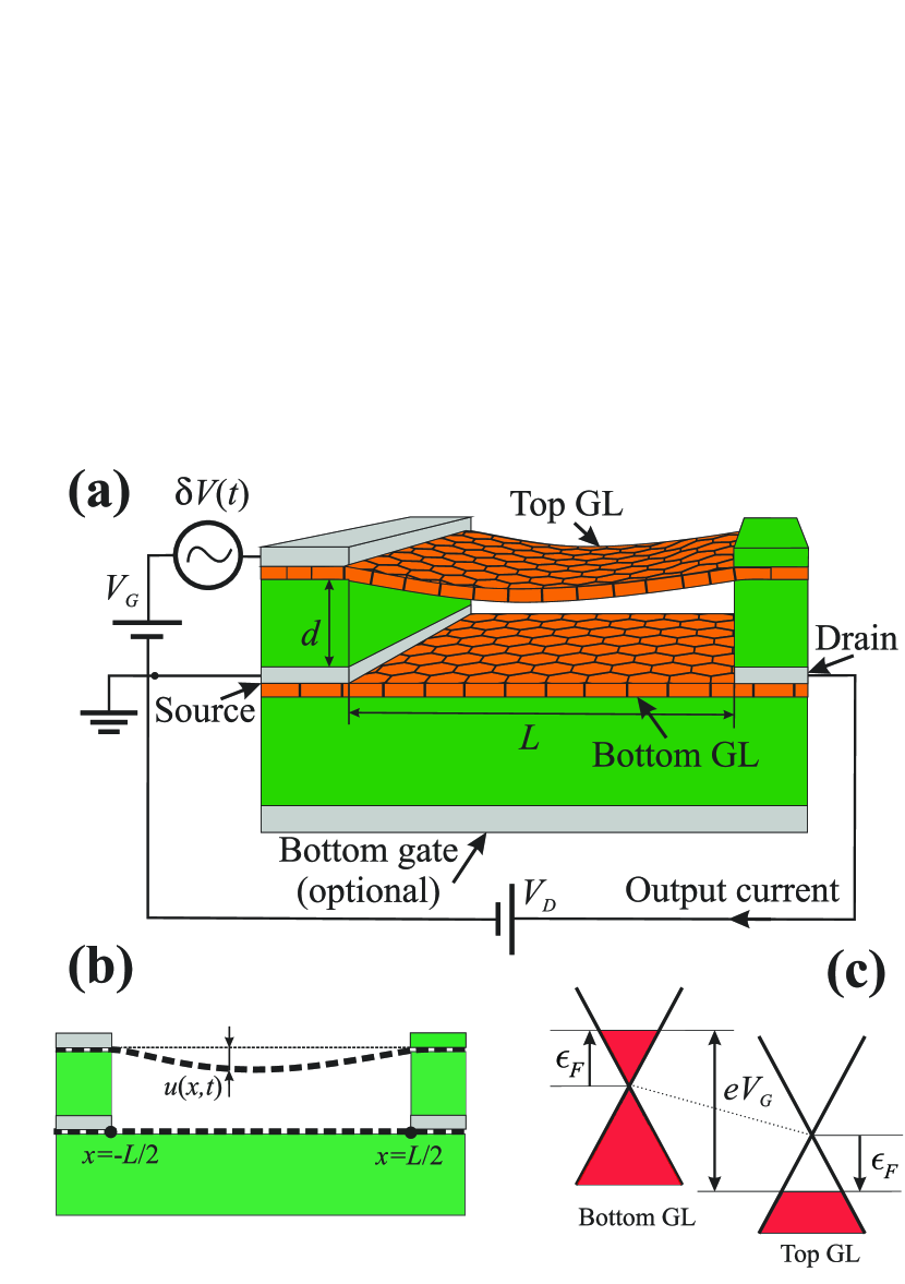
The proposed device structure represents a graphene FET with a mechanically floating gate made of graphene as well [figure 1 (a)]. The carrier signal is impinging on the structure or is delivered via a waveguide. The amplitude-modulated signal with the modulation frequency is applied between source and gate contacts. The carrier frequency is in the THz range being close to the Eigen frequency of the plasma oscillations. The modulation frequency is in the GHz range, which is close to the frequency of the top gate mechanical oscillations.
The carrier frequency excites plasma oscillations, which result in increasing the electric field strength between the top and bottom GLs. This, in turn, leads to a large ponderomotive force between them. The force spectrum contains the rectified component oscillating at the modulation frequency, which invokes mechanical oscillations of the graphene gate [figure 1 (b)]. The output signal of the detector is the ac source-drain current varying due to the changing gate-to-channel capacitance.
The THz demodulators exploiting combined plasma-mechanical resonance were first proposed in Refs. [16, 17, 18]. Those devices incorporated a conductive mechanically floating cantilever [16], nanowire or a nanotube [17] suspended over the channel of high-electron-mobility transistor. The structures of two aligned nanotubes were also studied [18]. The use of graphene in such kind of a device allows one to attain higher electron mobility, and thus a higher responsivity. Large breaking strain of graphene [5, 7] enables the gate rigidity tuning in a wide range, which is hardly possible for metallic cantilevers.
To estimate the plasma-wave response of the device, we apply the hydrodynamic equations for massless electrons and holes in graphene [19]. The mechanical vibrations are modelled using the elasticity theory equations for graphene membranes [20, 21]. We show that the resonant responsivity of modulated radiation detection is proportional to where and are the quality factors of mechanical and plasma resonators, respectively. We also show that the resonant amplitude of source-drain current oscillations is proportional to the third power of the electron mobility. Thus, the device responsivity appears to be large, reaching A/W in the resonant case. The gate voltage can effectively tune both the plasma and mechanical resonant frequencies. The optional bottom gate below the whole structure would allow for independent control of those frequencies. The device could be also used as an element of a mixer or a heterodyne detector if two THz frequencies are fed in and the difference is in resonance with the mechanical Eigen frequency. It can also operate as a detector of non-modulated THz radiation, with the responsivity by a factor of smaller than that in the case of the modulated radiation.
The paper is devoted to the analytical model describing the device output current and responsivity. Section II deals with the plasma-wave response of the structure. In Section III, the mechanical oscillations of the suspended graphene gate are considered. In Section IV, we estimate the output current of the device and its responsivity, and discuss possible generalizations of the considered structures. Section V contains the main conclusions.
2 Plasma-wave response
The proposed device consists of two GLs with the top layer being suspended over the bottom layer [figure 1 (a)]. The length and width of he layers are and , respectively, the distance between the GLs is . The gate voltage including a constant DC bias and the amplitude-modulated signal
| (1) |
is applied between left-side contacts to GLs ( is the modulation depth). A bias voltage (drain voltage) is applied across the bottom GL, allowing for dc current flow to be modulated by the incoming signal. The right contact to the top GL is eclectically isolated (or it could be connected to the top left contact).
Application of the DC gate voltage leads to the accumulation of electrons and holes in the opposite layers, as shown in figure 1 (c). In the absence of a built-in voltage, the Fermi energies of the electrons and holes are equal in modulus and opposite in sign. The electron and hole two-dimensional sheet densities are related to via a local capacitance relation
| (2) |
where is the effective specific capacitance corresponding to the series connection of geometric capacitance and quantum capacitances. The geometric capacitance per unit area is . The quantum capacitance, defined by [22] accounts for the dependence of the Fermi energy on the electric field strength between the GLs [figure 1 (c)]. For large distances between GLs ( nm at room temperature) or for high carrier densities is much larger than the geometric capacitance. At such conditions, , which will be assumed in the following.
Consider the plasma wave response of the transistor structure in figure 1 (a) to the application of a small harmonic signal at the left end of the top GL. The resulting voltage difference between the top and bottom layers, , is related to the perturbation of the charge density via
| (3) |
Combining the Ohm’s law with the continuity equations for the top and bottom GLs, we can relate the density perturbation to the perturbations of top and bottom layer potentials :
| (4) | |||
| (5) |
where and are the sheet conductivities of top and bottom GLs. The spatial variation of conductivity is assumed to be weak, which is valid at small drain voltage (i.e. in the linear mode of FET). Because of the equal carrier densities in the GLs and electron-hole symmetry . A slight deviation from this identity due to a stronger disorder in the bottom GL is possible. This issue will be briefly discussed later.
Combining (3), (4), and (5), we arrive at the equations governing the voltage distribution along the GLs
| (6) | |||
| (7) |
The boundary conditions imply constant ac voltage at the left edge of the top GL, zero ac voltage at both ends of bottom GL, and zero current at the isolated edge of top GL:
| (8) |
The quantity in Eqs. (6–7) has the dimensionality of the wave vector squared, we denote it by . Using the Drude-like expression for the graphene conductivity , where is the carrier collision frequency [19], we obtain the frequency dependence of :
| (9) |
where is the velocity of plasma waves in the gated graphene [14, 19]. Equations (6–7) are then rewritten as
| (10) | |||
| (11) |
Solving (10–11) with boundary conditions (8), we find the voltage difference between GLs
| (12) |
where is the dimensionless plasma resonant factor
| (13) |
and is the dimensionless function describing the spatial AC voltage distribution
| (14) |
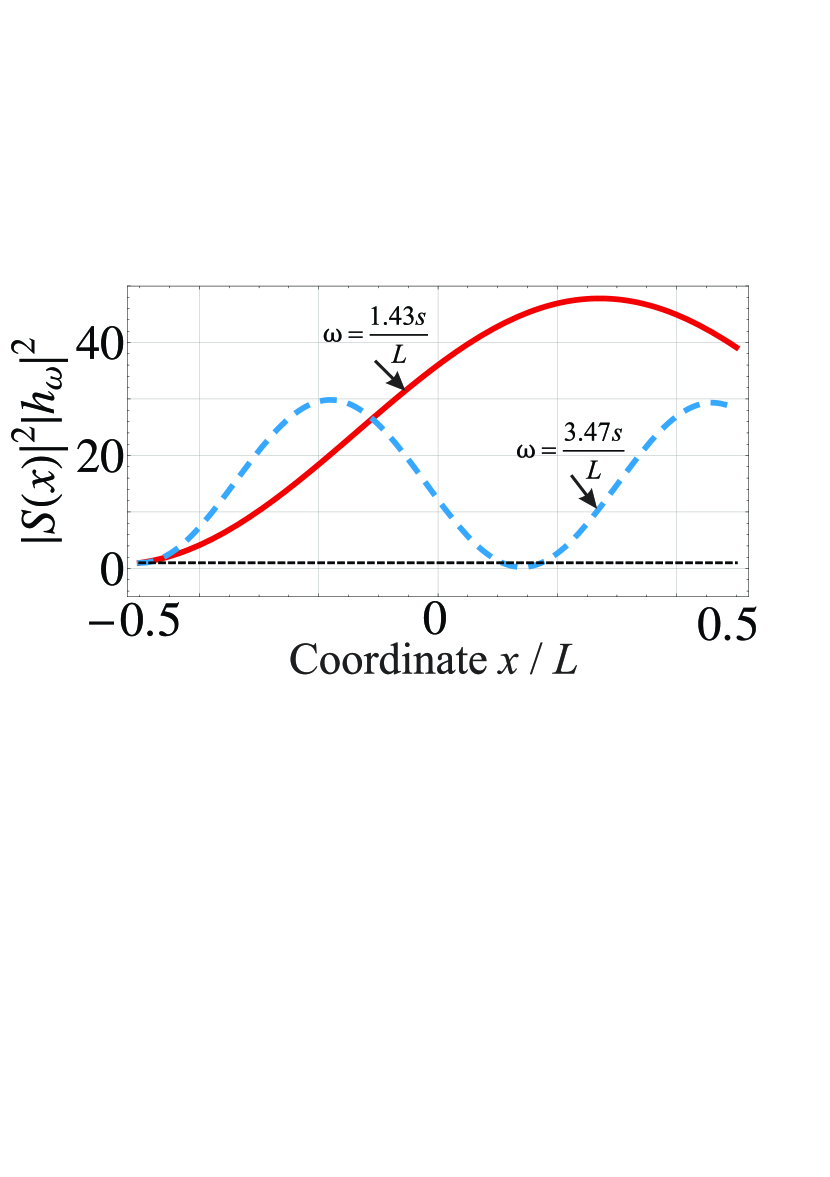
The spatial profiles of ponderomotive force proportional to are shown in figure 2 for the two first plasma resonances.
The resonant frequencies in the limit of weak damping are found from the solution of the transcendental equation , where . The first root of this equation, , corresponds to the plasma resonant frequency . In the vicinity of this resonance, is described by the Lorentz function
| (15) |
where we have introduced the quality factor of the plasma oscillations . For a typical value of the plasma wave velocity m/s which corresponds to the gate voltage of 2 V across the distance nm, the resonant frequency THz.
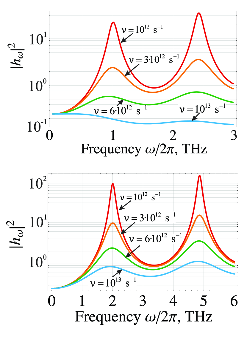
The magnitude and width of plasma resonance peaks are governed by the collision frequencies in the GLs. A careful analysis shows that if the collision frequencies in the top and bottom GLs are different, their average value appears in the expression for . In a suspended graphene layer, the collision frequency is quite small being limited by acoustic phonon scattering [9]. Provided , it can be estimated [23] as , where s-1. The collision frequency in the bottom GL is larger due to scattering on substrate defects. The reported [24] room-temperature electron mobility in graphene on boron nitride substrates is as high as cm(V s), which is only an order of magnitude lower than the mobility in suspended samples. In our calculations, we use the collision frequency as a free parameter, keeping in mind that the values reaching s-1 are possible. The plasma resonant curves in figure 3 are plotted for the two values of the length of the structure, m and nm, and for the collision frequencies varying from s-1 to s-1. Despite a rather low Q-factor ( for s-1 and m), the resonant detection is still pronounced.
Having obtained the plasma-wave response (12), we find the average ponderomotive force acting between the GLs (the averaging is performed over time ):
| (16) |
The first term in equation (2) is the attraction force due to the constant gate voltage . The second term is due to the varying distance between the electrodes at a fixed voltage. The third term is due to the rectification of the amplitude-modulated signal. It contains three harmonics: zero-frequency, which can be used for detection of non-modulated signals; the harmonic with the modulation frequency which leads to the forced oscillations of the top GL and invokes a mechanical resonance; and the double-frequency harmonic .
3 Mechanical response
The deflection, , of the suspended GL is found from the solution of the elasticity equations for graphene. According to the theory developed in Ref. [21], the bending energy of graphene is much less than its stretching energy. Thus, the time-dependent deformation of the GL is governed by the wave equation of the membrane oscillations. Presenting the deflection of the top GL as , where oscillates with the modulation frequency, , we write this equation as
| (17) |
Here, kg/m2 is the mass density of graphene, the frequency phenomenologically accounts for mechanical damping, and is the elastic force density. The latter is proportional to the tensile strain of the graphene layer:
| (18) |
where N/m is the two-dimensional elastic stiffness.
The first force term in the right-hand side of equation (3) is known to pull the resonant frequencies to lower values [7, 25]. We denote the corresponding frequency shift as (for V and nm MHz). Introducing the modified mechanical frequency and the velocity of transverse sound , we present equation (3) in a concise form
| (19) |
The solution of equation (19) with zero boundary conditions (clamped edges) is straightforward, moreover, for the estimate of change in gate-to-channel capacitance we need to know only the deflection averaged over -coordinate . The latter can be presented as
| (20) |
Here we have introduced the mechanical resonant factor . In the limit of weakly damped plasma oscillations, , it is given by the following expression
| (21) |
where , is the real part of , and its imaginary part is assumed to be small, are non-resonant factors,
| (22) |
The dependence of mechanical resonant factor provides a complicated pattern of resonances and anti-resonances appearing due to the spatial distribution of driving force (see figure 4). The principal resonant dependence is given by the term . In the vicinity of the first mechanical resonant frequency and plasma resonance, is described by the Lorentzian function
| (23) |
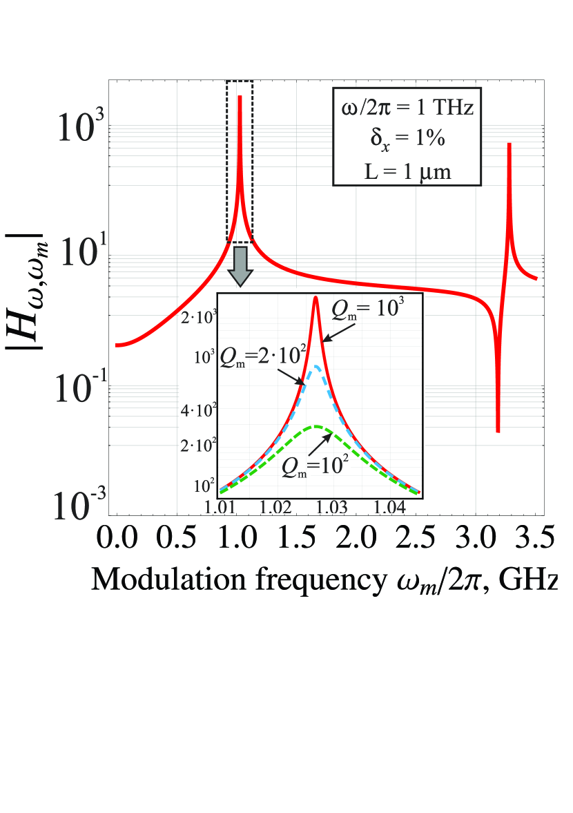
Here we have introduced the quality factor of mechanical resonator . The reported [7] room-temperature quality factors for the graphene resonators tuned to frequencies of hundred MHz are of the order of . In figure 4 we present the calculated mechanical response function for the tensile strain %, m, and quality factors ranging from to . These values correspond to the resonant frequency GHz. Higher frequencies are attainable for the all-clamped graphene structures and for GLs strained by a sufficiently large gate voltage.
4 Results: output current, responsivity, and tuning
Now we can estimate the amplitude of source-drain density resulting from the varying gate-to-channel capacitance. Provided that the FET operates in the linear mode (the constant drain voltage is smaller than the gate voltage ), is given by
| (24) |
where is the carrier mobility in the bottom GL. Using the obtained frequency dependence of the top GL deflection (20), we ultimately find
| (25) |
The quantity is the steady-state charge accumulated on a single GL per unit width , divided by the electron drift time from the source to the drain. Under the conditions of the combined plasma and mechanical resonance (), the detector current density is proportional to :
| (26) |
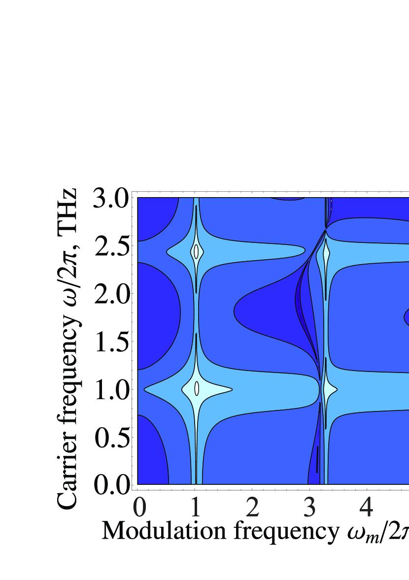
In figure 5, we plot the dependence of combined plasma-mechanical resonant factor on the carrier and modulation frequencies. It exhibits sharp peaks in the vicinity of and , with the resonant value exceeding . It follows from equation (26) that the current response is proportional to the third power of electron mobility (the second power comes from plasma quality factor squared and the first power comes from the drift time). Thus, the proposed device fully exploits the unique high-frequency electronic properties of graphene. The gate and channel in the proposed structure can be interchanged, so that the signal current flows in a suspended layer with enhanced electron mobility.
It should be noted that the proposed device can serve as a detector or non-modulated THz radiation. In this case, the rectified (zero-frequency) component of ponderomotive force would result in changing the DC source to drain current. The change in the DC current in the presence of a THz signal can be estimated as
| (27) |
which differs from Eq. (26) by the factor of .
Using Equations (26) and (27), we estimate the detector responsivity , where is the power of incoming THz radiation received by the antenna, and is the detector current. We use the typical parameters to attain the plasma and mechanical resonances at THz and GHz frequencies, respectively: m, nm, V, V, , , , . Relating to via
| (28) |
where is the antenna gain (for dipole antenna ), we obtain the responsivity of A/W for the detection of the modulated radiation, and A/W for detection of non-modulated radiation. The responsivity might be greatly enhanced by increasing due to a large non-linearity in the FET saturation regime.
Both plasma and mechanical resonant frequencies and can be tuned by application of the constant top gate voltage since it controls the electron and hole densities in the GLs [Eq. (2)] and their Fermi energies . The plasma wave velocity is . Thus, the plasma resonant frequency is a slowly increasing function of the gate voltage, . The dependence of the mechanical resonant frequency on is more complicated [8, 25]. On one hand, the application of the gate voltage increases and pulls the resonant frequency to lower values. However, at low voltages another factor is more important. The tensile strain of GL includes the built-in strain and voltage-induced strain , which is a growing function of .
Not going deep into mathematical details, we note that the addition of a back gate below the entire structure makes the independent tuning of mechanical and plasma resonances plausible. In this case, will still depend only on top gate voltage, , while the plasma wave velocity will be a function of both top and bottom gate voltages.
This device might also find applications as an extremely sensitive mass, gas [26] or biosensor [27]. The advantage in mass sensing compared to NEMs is a much larger area of a graphene gate compared to a nanowire or a nanotube. The sensing responsivity is also greatly enhanced in THz plasmonic devices [27] because of a high plasma wave sensitivity to changes in the electric field distribution caused by the sensed medium.
Finally, we note that for the operation of the proposed THz detector, low-resistivity contacts to graphene layers are required. Recently, contact resistances of Ohmm were reported for graphene/nickel contacts [28], while special treatment procedures can reduce this value down to – Ohmm [29, 30]. These values correspond to the recharging frequency of the order of s-1 for m and nm, which allows the device operation in the THz range.
5 Conclusions
We have proposed and substantiated the operation of a resonant detector of the THz radiation modulated by GHz-signals. The device uses a graphene field-effect transistor with mechanically floating graphene gate. The THz component of incoming radiation invokes plasma resonance in the graphene layers, thus leading to a high ponderomotive force. The component of the ponderomotive force oscillating with the modulation frequency excites mechanical vibrations of the graphene gate. This leads to the change in the source-drain current. The resonant responsivity is proportional to . For the structures that are m long, the values and look feasible. Frequencies of both plasma and mechanical oscillations can be tuned by a constant gate voltage.
Acknowledgement
The work at RIEC was supported by the Japan Society for Promotion of Science (JSPS Grant-in-Aid for Specially Promoting Research 23000008), Japan. The work of D.S. was supported by the JSPS Postdoctoral Fellowship for Foreign Researchers (Short-term), Japan. The work of V.L. was supported by the Russian Foundation for Basic Research (grants # 12-07-00710, 12-07-00592, and 13-07-00270). The work at RPI was supported by the US Army Cooperative Research Agreement (Program Manager Dr. Meredith Reed).
6 References
References
- [1] Nathanson H C, Newell W E, Wickstrom R A, and Davism J R 1967 IEEE Trans. El. Dev. 14 117
- [2] Gad-el-Hak M MEMS: introduction and fundamentals CRC press 2010
- [3] Feng P. X.-L. 2013 Nature Nanotechnol. 8 897-8
- [4] Sazonova V, Yaish Y, Üstünel H, Roundy D, Arias T A, McEuen P L 2004 Nature 431 284-7
- [5] Lee C, Wei X, Kysar J W, Hone J 2008 Science 321 385-8
- [6] Lee S, Chen C, Deshpande, Deshpande V V, Lee G-H, Lee I, Lekas M, Gondarenko A, Yu Y-J, Shepard K, Kim P, Hone J 2013 Appl. Phys. Lett. 102 153101
- [7] Chen C and Hone J 2013 Proc. IEEE 101 1766-79
- [8] Chen C, Lee S, Deshpande V V, Lee G-H, Lekas M, Shepard K, Hone J 2013 Nature Nanotechnol. 8 923-7
- [9] Bolotin K I, Sikes K J, Jiang Z, Klima M, Fudenberg G, Hone J, Kim P, Stormer H L 2008 Solid State Comm. 146 351-5
- [10] Zheng J, Wang L, Quhe R, Liu Q, Li H, Yu D, Mei W-N, Shi J, Gao Z, Lu J 2013 Scientific Reports 3 1314
- [11] Liu M, Yin X, Ulin-Avila E, Geng D, Zentgraf T, Ju L, Wang F, Zhang X 2011 Nature 474 64-7
- [12] Ryzhii V, Otsuji T, Ryzhii M, Leiman V G, Yurchenko S O, Mitin V, Shur M S 2012 J. Appl. Phys. 112 104507
- [13] Muraviev A V, Rumyantsev S L, Liu G, Balandin A A, Knap W, Shur M S 2013 Appl. Phys. Lett. 103 181114
- [14] Ryzhii V, Satou A, Otsuji T 2007 J. Appl. Phys. 101 024509
- [15] Dyakonov M and Shur M S 1996 IEEE Trans. El. Dev. 43 380-7
- [16] Ryzhii V, Ryzhii M, Hu Y, Hagiwara I, Shur M S 2007 Appl. Phys. Lett. 90 203503
- [17] Leiman V G, Ryzhii M, Satou A, Ryabova N, Ryzhii V, Otsuji T, Shur M S 2008 J. Appl. Phys. 104 024514
- [18] Stebunov Y, Leiman V G, Arsenin A, Gladun A, Semenenko V, Ryzhii V 2011 Appl. Phys. Express 4 075101
- [19] Svintsov D, Vyurkov V, Yurchenko S, Ryzhii V, Otsuji T 2012 J. Appl. Phys. 111 083715
- [20] L.D. Landau and E.M. Lifshitz. Theory of Elasticity. Pergamon Press, 1970.
- [21] Atalaya J, Isacsson A, Kinaret J M 2008 Nano. Lett. 8 4196-200
- [22] Luryi S 1988 Appl. Phys. Lett. 52 501-3
- [23] Vasko F T and Ryzhii V 2007 Phys. Rev. B 76 233404
- [24] Meric I, Dean C R, Petrone N, Wang L. 2013 Proc. IEEE 101 (7) 1609-1619
- [25] Solanki H S, Sengupta S, Dhara S, Singh V, Patil S, Dhall R, Parpia J, Bhattacharya A, Deshmukh M M 2010 Phys. Rev. B 81 115459
- [26] Rumyantsev S, Liu G, Shur M S, Potyrailo R A, Balandin A A 2012 Nano Lett. 12 2294-98
- [27] Pala N and Shur M S 2008 Electronics Letters 44 1391-3
- [28] Nagashio K, Nishimura T, Kita K, Toriumi A 2009 IEEE International Electron Devices Meeting (IEDM) 1-4
- [29] Leong W Sun, Gong H, Thong J T L 2014 ACS Nano 8 994-1001
- [30] Li W, Liang Y, Yu D, Peng L, Pernstich K P, Shen T, Hight Walker, A R, Cheng G, Hacker C A, Richter C A, Li Q, Gundlach D J, Liang X 2013 Appl. Phys. Lett. 102 183110