Controlling the 2DEG states evolution at a metal/Bi2Se3 interface
Abstract
We have demonstrated that the evolution of the two-dimensional electron gas (2DEG) system at an interface of metal and the model topological insulator (TI) Bi2Se3 can be controlled by choosing an appropriate kind of metal elements and by applying a low temperature evaporation procedure. In particular, we have found that only topological surface states (TSSs) can exist at a Mn/Bi2Se3 interface, which would be useful for implementing an electric contact with surface current channels only. The existence of the TSSs alone at the interface was confirmed by angle-resolved photoemission spectroscopy (ARPES). Based on the ARPES and core-level x-ray photoemission spectroscopy measurements, we propose a cation intercalation model to explain our findings.
*E-mail: ffnhj@chonnam.ac.kr
Since the discovery of topological insulators (TIs) with topologically protected metallic surface statesFu1 ; Noh1 ; Hsieh1 ; Xia ; HZhang ; Hsieh2 , much attention has been paid to characterization of the topological surface states (TSSs), unveiling the abundant exotic properties of the TSSs such as the absence of back-scatteringRoushan ; TZhang , the spin-momentum lockingHsieh2 ; Pan , the robustness against various kinds of surface perturbationsPark1 ; Noh2 ; Valla1 ; Wray . In particular, the studies on the effect of surface adsorbates to the TSSs have found very intriguing phenomena that new Rashiba-type spin-split surface states emerge on the (111) surface of Bi2Se3 TI and that they have large amounts of common features irrespective of the electric/magnetic properties of the adsorbatesValla1 ; King ; Benia . The successive experimental and theoretical studies have suggested that the newly emerging surface states are actually interface states in a quantum-confined two-dimensional electron gas (2DEG) induced by a surface band-bending effectBianchi ; Bahramy ; Mann .
The coexistence of TSSs and 2DEG states is a very exotic example in a viewpoint of surface physics and have potential applications in the field of nanoscale spintronic devices, so the understanding of their origin and properties is essential in this TI physics. However, the newly developed 2DEG has a complex spin-orbit-split electronic structure, which could be an obstacle depending on the way how to implement TI-based devices. For example, when we want to use an electric current through only the TSSs in Bi2Se3 or when we want to make an n-type TI-metal junction whose current channel is only TSSs, those 2DEG states are definitely to be removed. In spite of these practical needs, all reports on the effects of adsorbates or surface impurities on Bi2Se3 surfaces have only shown that the 2DEG states are easily formed by various kinds of adsorbates in an ultra-high vacuum, but have not suggested a possible way to remove the developed 2DEG states without killing the TSSs.
In this study, we focus on this issue and performed systematic angle-resolved photoemission spectroscopy (ARPES) measurements in order to explore whether there is a way to remove the 2DEG states with leaving the TSSs alone at a metal/Bi2Se3 interface. Keeping in mind that the practicality of the surface states described above appears at an interface between metal and TI, we deposited in situ several kinds of metal elements such as Cu, In, and Mn on a (111) surface of Bi2Se3 in a well-controlled manner, which actually corresponds to an early stage of a metal thin film synthesis, and observed an evolution/devolution of the TSSs and 2DEG states as a function of deposition thickness by ARPES and core-level x-ray photoemission spectroscopy (XPS). Our ARPES measurements reveal that in the case of Cu and In, the 2DEG states are developed with a Rashiba-type spin-split electronic structure and are saturated up to 1 monolayer (ML), but that in the case of Mn, the 2DEG states are developed up to 0.4 ML, then disappear above 1.0 ML. The disappearance of the 2DEG states and the existence of the TSSs alone were observed on a Bi2Se3 (111) surface covered with up to 10 ML of Mn atoms by ARPES, indicating that only the TSSs exist at the Mn/Bi2Se3 interface prepared by our procedure. In order to explain why Mn deposition makes a difference from Cu or In deposition, we kept track of the XPS spectral changes for Bi 4, Se 4, and Cu/In/Mn core levels, and proposed a cation intercalation model where the intercalated cations act as a potential gradient reducer.
.1 Results
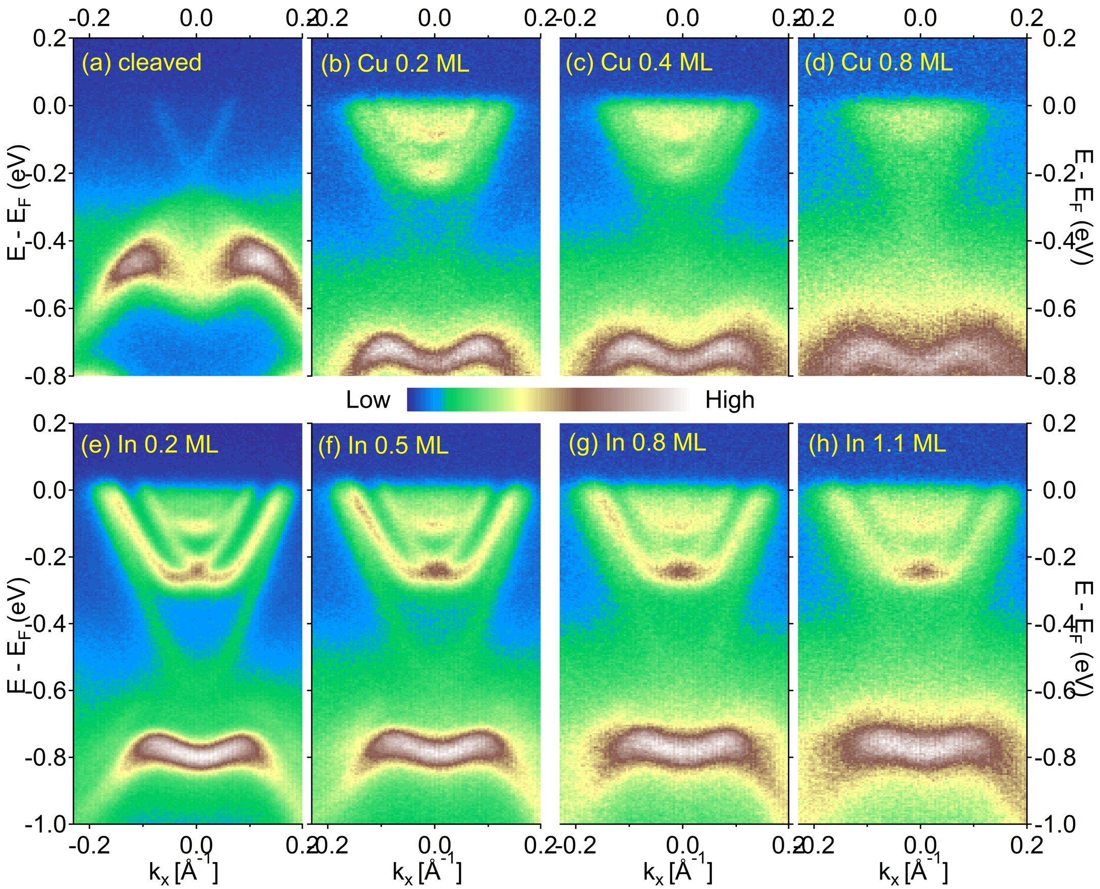
Typical features of the TSSs in a fresh (111) surface of Bi2Se3 are presented in Fig. 1(a). The ARPES image was obtained along the direction within 15 minutes after cleaving the sample at 40 K during which we did not observe any aging effect due to the adsorption of residual gas molecules in the vacuum chamber. This is quite different from the p-doped Bi2Te3 case in our previous reportNoh1 . The V-shaped linear dispersive surface bands form two Dirac cones sharing the Dirac point (DP) located at around 200 meV below the Fermi level. Below the DP, a clear M-shaped bulk valence band is seen. On this cleaved surface, we deposited copper or indium atoms in situ by evaporating pure (99.999%) copper or indium metal with a well-controlled manner described below. Figures 1(b)-1(d) show an evolution of the TSSs and the 2DEG states as a function of Cu deposition thickness. At a small amount of Cu deposition (0.2 ML), newly developed surface states with Rashiba-type spin-splittings are clearly seen together with the TSSs. The DP and the M-shaped valence bands shift to the higher binding energy side by 0.3 eV. In Figs. 1(e)-1(h), a similar surface state evolution is displayed with the increase of In deposition. A prominent difference from the Cu deposition case appears in the size of the Rashba-type spin splittings, but both cases share common features in many aspects. The similar behavior of the surface state evolution has been reported for various kinds of surface deposition or surface adsorptionBenia ; Valla1 . However, the development of the surface states does not originate from a topological property of TIs but from an interface property of metal/semiconductor. In the case of Bi0.9Sb0.1 TI, our previous ARPES study shows just a small shift of the Fermi level in the electronic structure with response to the surface adsorptionNoh2 .
The origin of these surface states emerging in the (111) surface of Bi2X3 (X=chalcogen) compounds has proved controversial initially, but one of the most persuasive models argues that those are a kind of 2DEG states developed in a 2-dimensional quantum well which is induced by a strong band bending at a metal/semiconductor interfaceNoh1 ; Wray ; King ; Bianchi ; Bahramy . According to this scenario, the dominant factors for the 2DEG states are the shape of the potential profile as a function of depth from the interface and the induced charge density at the interface, but the kinds and the amount of adsorbates are not important if only they stick on the surface to form a well-defined interface. Thus, in order to remove the 2DEG states at a metal/Bi2Se3 interface, or at least in order to make a different surface electronic structure from the prototypical 2DEG states, metal elements that can intercalate or be interstitial defects are expected to be more effective. In this viewpoint, one different behavior between Cu- and In-depositions can be qualitatively understood. At relatively thick deposition (0.8 ML), the 2DEG states look more shrunk in the Cu-deposited sample than in the In-deposited sample as shown in Figs. 1(d) and 1(g). This is possibly due to the intercalatability difference between Cu and In atoms for Bi2Se3. Actually, it has been reported that Cu atoms can intercalate into the van der Waals (vdW) gaps in Bi2Se3, while there is no such report for In atoms to our knowlegeWang .
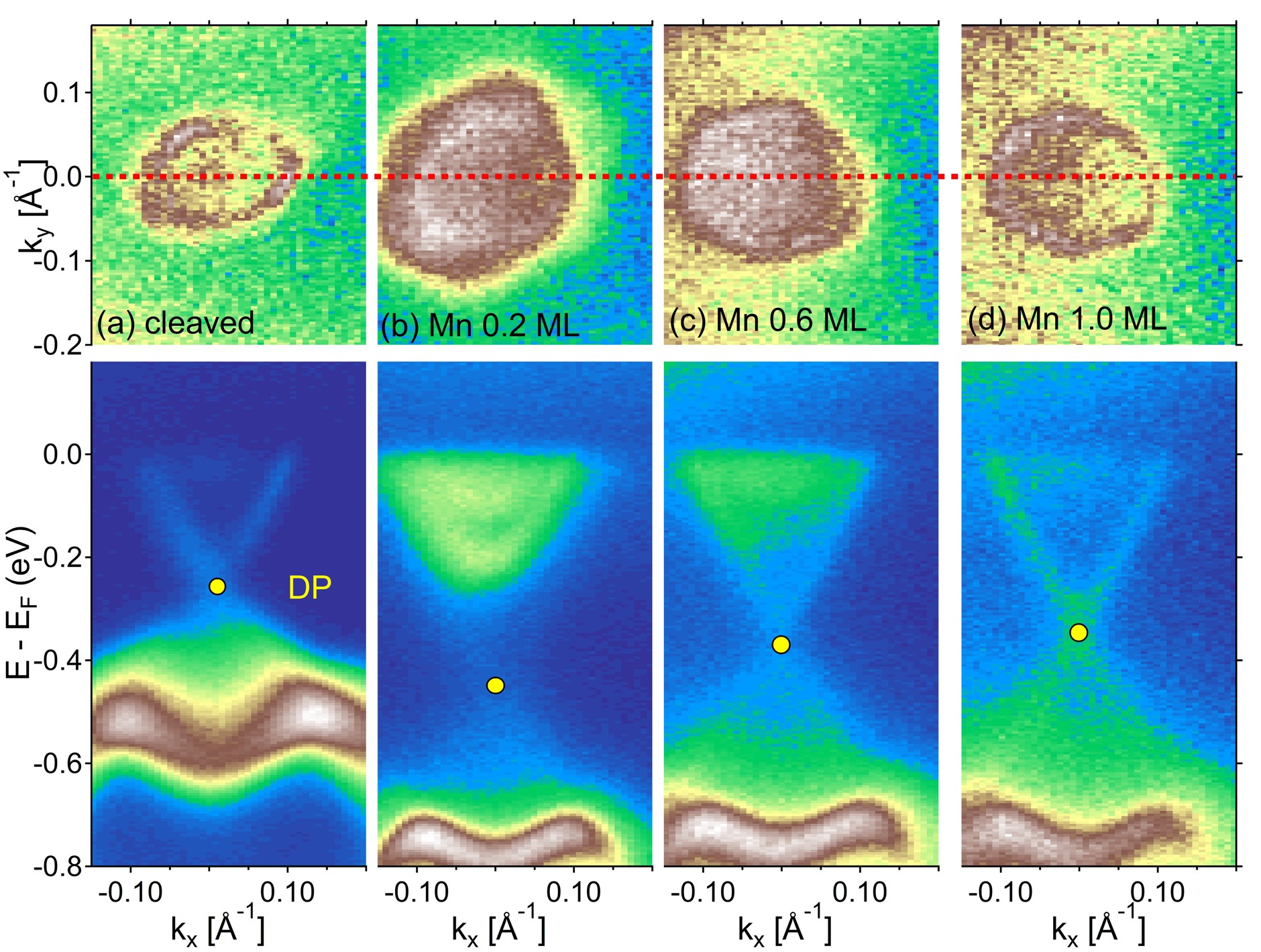
Keeping in mind that the intercalatability of the deposited atoms may be the crucial factor for our purpose, we chose Mn as a deposition material and kept track of the 2DEG states evolution as a function of deposition thickness since it is known that a small amount of Mn can be doped in Bi2Se3Cho . Rubidium was also reported to intercalate into the gap, but its effect on the 2DEG states lies in another direction to our purposeBianchi2 . Figures 2(a)-2(d) show the ARPES-measured Fermi surface (upper panel) and the corresponding energy dispersion relation (lower panel) along the red dotted line (approximately direction) for a clean surface, 0.2 ML, 0.6 ML, and 1.0 ML Mn-deposited surface, respectively. Interestingly enough, Mn-deposited surfaces show a very different evolution of the 2DEG states. At a small amount of Mn deposition (0.2 ML), quite a complex 2DEG structure is developed as shown in Fig. 2(b). It looks similar to that of the Cu-deposited surface. However, when the deposited layer is thicker than 0.2 ML, the Fermi surface (FS) size of the 2DEG states becomes smaller, and the DP shifts up by 0.1 eV as is shown in Fig. 2(c). At around Mn 1.0 ML, the 2DEG states almost disappear and only the TSSs remain as can be seen in Fig. 2(d). Based on the facts that the energy position of the DP in Mn 1.0 ML deposition is 0.1 eV deeper than that of the clean surface and that the size of the hexagonal FS of the TSSs is a little larger than that of the clean surface, the surface does not recover to its original condition, but forms another interface that gives a similar environment to the original vacuum/(111) interface for the TSSs and 2DEG.
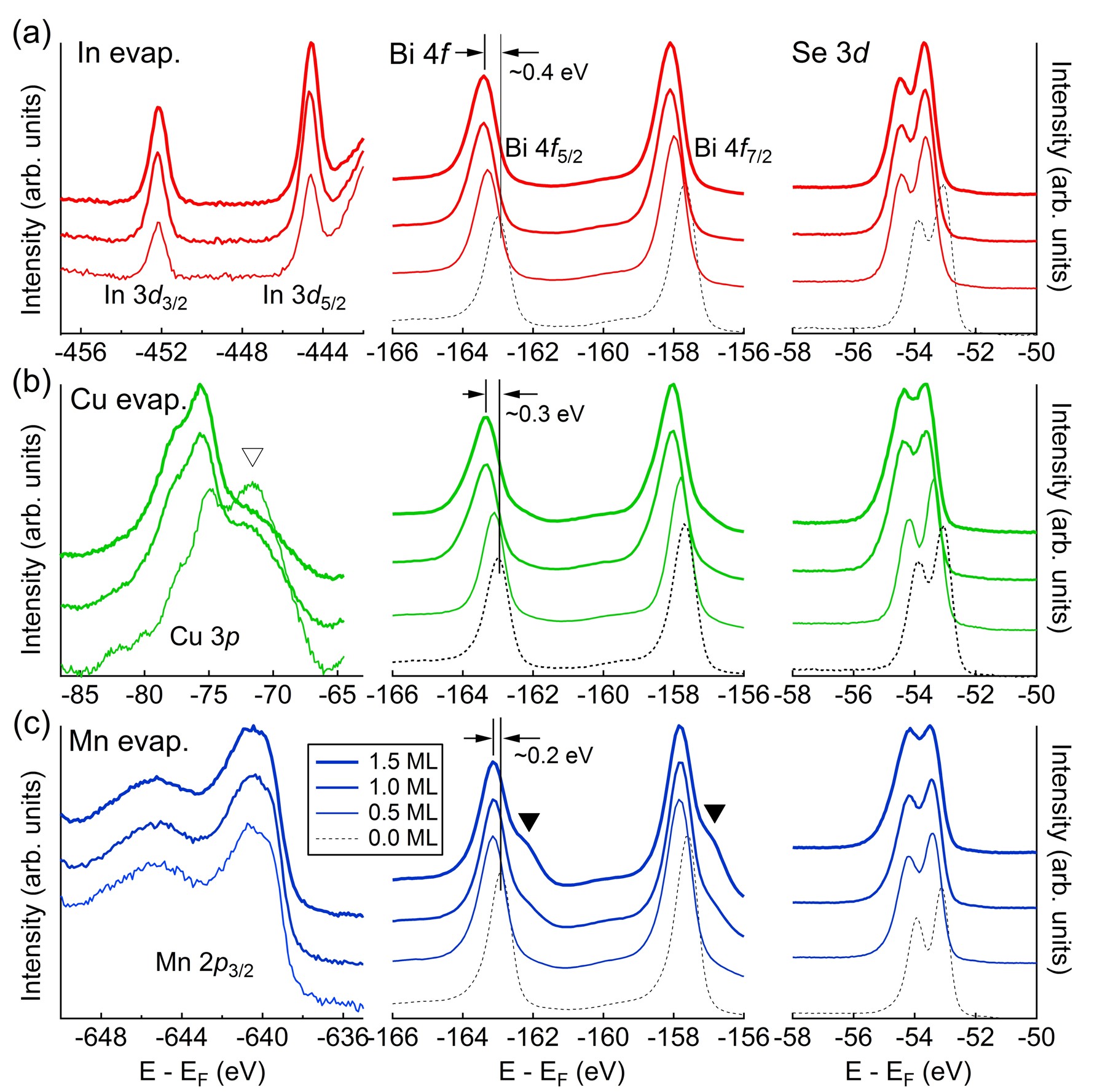
In order to figure out why the Mn deposition makes such an intriguing behavior in the 2DEG states evolution, we carried out core-level XPS measurements as is displayed in Fig. 3. Since XPS is sensitive to the chemical valency and chemical environment of ions in solids, important information or at least a clue on the reason of the disappearance of the 2DEG states can be obtained by analyzing the XPS spectra. In the left column, the center one, and the right one of Fig. 3, the XPS spectra of each deposited element core level, Bi 4, and Se 3 level are presented with the increase of the deposition thickness, respectively. In the case of In deposition, the Bi 4 and Se 3 peaks shift toward lower kinetic energy side by 0.4 eV with the increase of the deposition thickness as shown in Fig. 3(a). The amount of the energy shift corresponds to the band bending shown in Figs. 1(a) and 1(h), so it can be interpreted as a surface potential shift due to the accumulated surface charge induced by the In deposites. The similar core-level shifts are observed in the Cu- and Mn-deposited surface, respectively, as is shown in Figs. 3(b) and 3(c), and the amount of energy shift is also very consistent with that of the band shift in Figs. 1 and 2.
Several interesting features in the core-level spectra of each deposited element, Bi 4, and Se 3 are found in a different dependence on deposition. While In deposition does not make any change in the In 3, Bi 4, and Se 3 spectral line shape, Cu(Mn) deposition induces an evolution in Cu 3 (Mn 2), Bi 4, and Se 3 level, respectively. In the Cu 3 region, two doublets (75 eV and 71 eV) are observed, each of which can be assigned to surface peak and intercalation peak() as shown in Fig. 3(b). The relative peak weight dependence on deposition thickness strongly supports this assignment, and the similar result has been reported in the Rb deposition/annealing studyBianchi2 . Meanwhile, Mn 2 do not make a prominent difference in their shape with the amount of Mn deposition, so it is not clear whether a part of the adsorbated Cu atoms intercalates or not. However, Mn deposition effects on the other core level spectra are not similar to the indium case. For both Cu and Mn deposition cases, a new spectral weight appears between the spin-orbit-split peaks of the Se 3 together with the increase of the peak width. This indicates an occurrence of another kind of Se ions chemically different from those in pristine Bi2Se3. The similar evolutionary behavior is observed in the Bi 4 region () of Fig. 3(c). The prominent evolution of the Bi 4 peaks in the Mn-deposited surface is quite contrastive to the Cu case where the Bi 4 peaks hardly show the dependence on the Cu deposition thickness. This element-specific response to the deposites indicates that intercalatability and intercalated sites of the deposites into Bi2Se3 bulk are different among In, Cu and Mn. The invariance of the XPS spectra in the In-deposited surface suggests that In atoms do not intercalate into the Bi2Se3 bulk. Meanwhile, a part of the Cu or Mn deposites definitely intercalate into the bulk but their intercalated sites are different. Based on the Bi 4 and Se 3 XPS spectra, the intercalated Cu atoms affect on the Se anions only. Meanwhile, the intercalated Mn atoms affect on the Bi ions as well as the Se ions. This contrastive response suggests that the intercalated Cu atoms reside mainly in the vdW gaps between the quintuple layers (QLs) while the Mn atoms are in the interstitial sites as well as in the vdW gaps. This also explains why the binding energy of the intercalated Cu atom 3 levels is smaller than that of the deposited Cu atoms on the surface. Since the QLs are chemically very stable and electrically close to neutral, the intercalated atoms into the vdW gaps are also very close to charge-neutral, so the binding energy of the atoms is smaller than that of Cu metal which is close to monovalent ion. The zero valence of the intercalated Cu ions into the vdW gaps of Bi2Se3 has been reported in an electron energy loss spectroscopy studyKoski . Meanwhile, the interstitial Mn atoms are likely to act as cations as Bi atoms do. If this is the case, the intercalated Mn cations cannot help making moderate the surface band bending effect induced by the deposited Mn adsorbates.
.2 Discussion
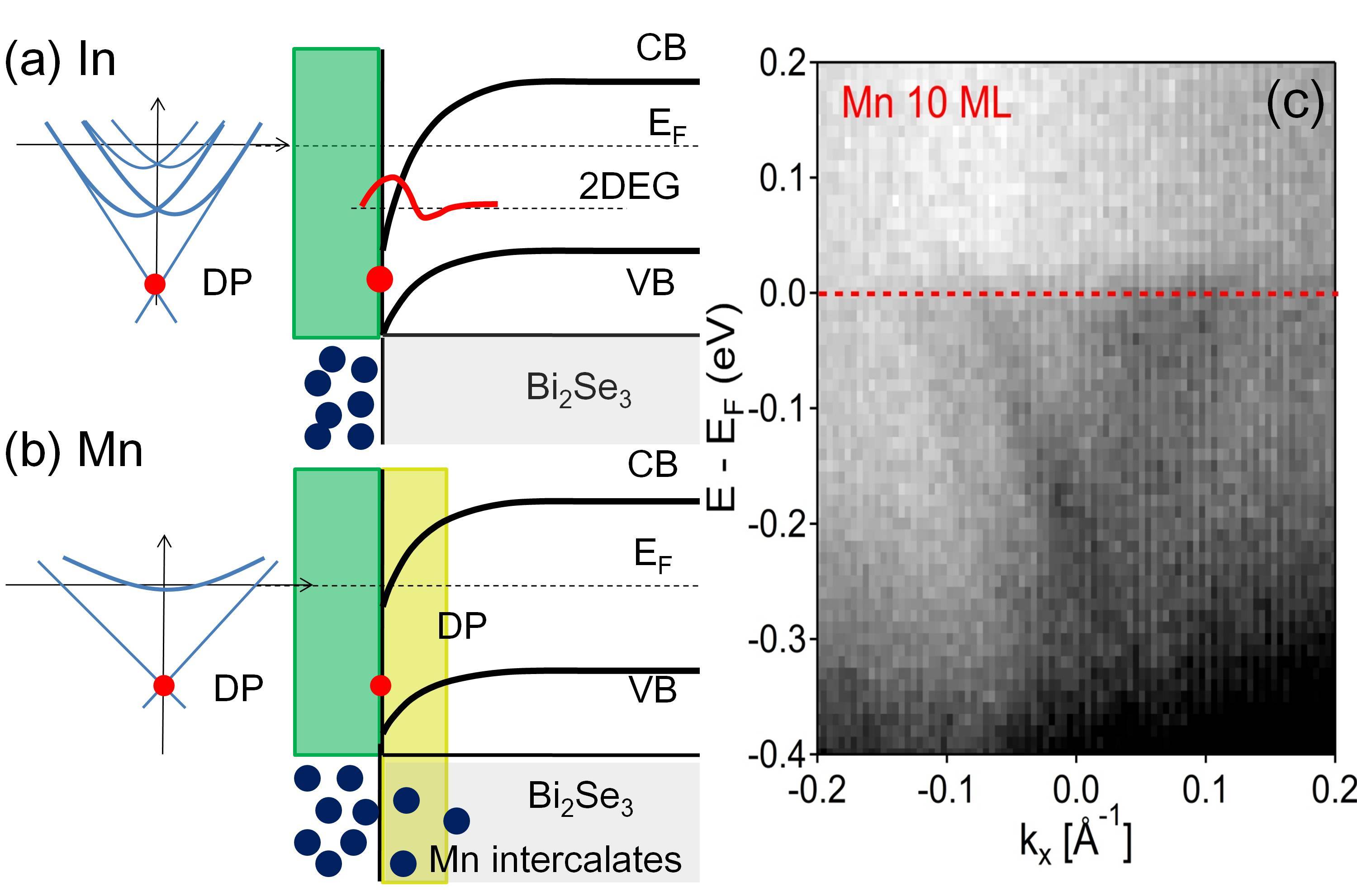
The XPS measurements described above give important information to explain the 2DEG states appearance/disappearance in our ARPES data. Probably, the most simple way to the 2DEG removal is to weaken the adsorbates-induced band bending at the interface. We have evidenced in the XPS study that the Mn adsorbates intercalate into the interstitial sites as well as the vdW gap between the QLs of Bi2Se3 and make the surface potential gradient more gentle, acting as a buffer. Although most of the intercalated Mn atoms stay charge neutral, a part of them gives a few electrons per atom and act as Mn cations, so the surface potential gradient gets smaller as the average intercalation depth gets larger. Figures 4(a) and 4(b) show a schematic configuration for our cation intercalation model. In the case of In deposition, the surface charges induced by the deposited indium ions attract electrons toward the In/Bi2Se3 interface, making a 2DEG system. When there are no intercalating indium ions, a deep well-like surface potential forms at the interface, developing 2DEG states with a complex Rashba-type spin-splitting structure. However, as in the case of Mn deposition, if parts of the deposited Mn atoms intercalate into the interstitial sites of Bi2Se3, and are ionized into Mn cations, the deep well-like surface potential changes to a wide valley with a gentle slope. In this model, the different response to Cu deposition is also naturally explained. As is described above, Cu atoms are also known to intercalate into the vdW gap, but they do not intercalate into the interstitial sites, so almost all of the intercalated Cu atoms stay charge neutral. The lower binding energy of the intercalated Cu 3 peak in Fig. 3(b) supports this interpretation. Actually, if we compare the Cu and In deposition results, the 2DEG states in the Cu deposition shrink a little more than those in the In deposition (See Fig. 1(d) and (g)). So, the Cu intercalation effects definitely exist, but are not so prominent like the Mn case. This is due to a smaller fraction of the ionized Cu atoms to the intercalated ones than that of Mn atoms.
Finally, we have checked whether the TSSs still exist even in an environment that can be regarded as a real metal/TI interface. In Fig. 4(c), the ARPES image shows dim V-shape TSSs near the Fermi level. This image was obtained from a 10 ML Mn-deposited Bi2Se3 (111) surface. Since the scattering rate of the photoelectrons is very high due to the thick Mn layers, the ARPES-measured TSSs look very blurred, but definitely we can see the existence of the TSSs alone at the interface.
.3 Experimental methods
The Bi2Se3 single crystals were grown by the melting method. The stoichiometric mixture of Bi(99.999) and Se(99.9999) was loaded in a evacuated quartz ampoule. The ampoule was heated up to 850∘C for 48 hours, followed by slow cooling to 500∘C at a rate of 2∘C/h. The furnace was kept at this temperature for 5 additional days for post-annealing before furnace cooling. The ARPES and XPS experiments were performed at the 4A1 beamline of the Pohang Light Source with a Scienta SES-2002 electron spectrometer and =25 and 800 eV photonsHDKim . The total energy (momentum) resolution is 20 meV (0.01 Å-1) for ARPES and 0.8 eV for XPS. The crystals were cleaved in situ by the top-post method at 40 K under Torr. Surface adsorbates/intercalates were introduced on the sample surfaces by evaporating the pure (99.999%) metal elements with a rate of 0.1 Å/min in an ultra-high vacuum of 1.010-10 Torr at 50 K of the sample temperature.
.4 References
References
- (1) Fu, L., Kane, C. L. & E. J. Mele, Topological Insulators in Three Dimensions. Phys. Rev. Lett. 98, 106803 (2007).
- (2) Noh, H.-J. et al. Spin-orbit interaction effect in the electronic structure of Bi2Te3 observed by angle-resolved photoemission spectroscopy. Europhys. Lett. 81, 57006 (2008).
- (3) Hsieh D. et al. A topological Dirac insulator in q quantum spin Hall phase. Nature 452, 970 (2008).
- (4) Xia, Y. et al. Observation of a large-gap topological-insulator class with a single Dirac cone on the surface. Nat. Phys. 5, 398 (2009).
- (5) Zhang, H. et al. Topological insulators in Bi2Se3, Bi2Te3, and Sb2Te3 with a single Dirac cone on the surface. Nat. Phys. 5, 438 (2009).
- (6) D. Hsieh et al. Observation of Unconventional Quantum Spin Textures in Topological Insulators. Science 323, 919 (2009).
- (7) Roushan, P. et al. Topological surface states protected from backscattering by chiral spin texture. Nature 460, 1106 (2009).
- (8) Zhang, T. et al. Experimental Demonstration of Topological Surface States Protected by Time-Reversal Symmetry. Phys. Rev. Lett. 103, 266803 (2009).
- (9) Pan, Z.-H. et al. Electronic Structure of the Topological Insulator Bi2Se3 Using Angle-Resolved Photoemission Spectroscopy: Evidence for a Nearly Full Surface Spin Polarization. Phys. Rev. Lett. 106, 257004 (2011).
- (10) Park, S. R. et al. Quasiparticle scattering and the protected nature of the topological states in a parent topological insulator Bi2Se3. Phys. Rev. B 81, 041405 (2010).
- (11) Noh, H.-J. et al. Persistence of surface states despite impurities in the surface of topological insulators. Europhys. Lett. 96, 47002 (2011).
- (12) Valla, T. et al. Photoemission Spectroscopy of Magnetic and Nonmagnetic Impurities on the Surface of the Bi2Se3 Topological Insulator. Phys. Rev. Lett. 108, 117601 (2012).
- (13) Wray, L. A. et al. A topological insulator surface under strong Coulomb, magnetic and disorder perturbations. Nat. Phys. 7, 32 (2011).
- (14) King, P. D. C. et al. Large Tunable Rashba Spin Splitting of a Two-Dimensional Electron Gas in Bi2Se3. Phys. Rev. Lett. 107, 096802 (2011).
- (15) Benia, H. M. et al. Reactive Chemical Doping of the Bi2Se3 Topological Insulator. Phys. Rev. Lett. 107, 177602 (2011).
- (16) Bianchi, M. et al. Coexistence of the topological state and a two-dimensional electron gas on the surface of Bi2Se3. Nature Commun. 1, 128 (2010).
- (17) Bahramy M. S. et al. Emergent quantum confinement at topological insulator surfaces. Nature Commun. 3, 1159 (2012).
- (18) Mann, C. et al. Mapping the 3D surface potential in Bi2Se3. Nature Commun. 4, 2277 (2013).
- (19) Wang, Y.-L. et al. Structural defects and electronic properties of the Cu-doped topological insulator Bi2Se3. Phys. Rev. B 84, 075335 (2011).
- (20) Choi, J. et al. Magnetic and transport properties of Mn-doped Bi2Se3 and Sb2Se3. J. Magnetism and Magnetic Materials 304, e164 (2006).
- (21) Bianchi, M. et al. Robust Surface Doping of Bi2Se3 by Rubidium Intercalation. ACS Nano 6, 7009 (2012).
- (22) Koski, K. J. et al. High-Density Chemical Intercalation of Zero-Valent Copper into Bi2Se3 Nanoribbons. J. Am. Chem. Soc. 134, 7584 (2012).
- (23) Kim, H.-D. et al. Performance of a Micro-Spot High-Resolution Photoemission Beamline at PAL. AIP Conf. Proc. 879, 477 (2007).
.5 Acknowledgments
This work was supported by the National Research Foundation (NRF) of Korea Grant funded by the Korean Government (MEST) (Nos. 2010-0010771 and 2013R1A1A2058195), by the NRF through the SRC Center for Topological Matter (No. 2011-0030046) and the Mid-Career Researcher Program (No. 2012-013838), and by the IBS in Korea. The experiments at PLS were supported in part by MSIP and POSTECH.
.6 Competing financial interests
The authors declare no competing financial interests.
.7 Author contributions
The whole research was planned by H.J.N. Bi2Se3 crystals were grown by J.P. and J.S.K. ARPES/XPS measurements were carried out by J.J., I.K, E.J.C., B.G.P., H.D.K., and H.J.N. H.J.N wrote the paper with suggestions and comments by H.D.K., E.J.C., and J.S.K.