Front-End Board with Cyclone® V as a Test High-Resolution Platform for the Auger_Beyond_2015 Front End Electronics
Abstract
The surface detector (SD) array of the Pierre Auger Observatory containing at present 1680 water Cherenkov detectors spread over an area of 3000 km2 started to operate since 2004. The currently used Front-End Boards are equipped with no-more produced ACEX® and obsolete Cyclone® FPGA (40 MSps/15-bit of dynamic range).
Huge progress in electronics and new challenges from physics impose a significant upgrade of the SD electronics either to improve a quality of measurements (much higher sampling and much wider dynamic range) or pick-up from a background extremely rare events (new FPGA algorithms based on sophisticated approaches like e.g. spectral triggers or neural networks). Much higher SD sensitivity is necessary to confirm or reject hypothesis critical for a modern astrophysics.
The paper presents the Front-End Board (FEB) with the biggest Cyclone® V E FPGA 5CEFA9F31I7N, supporting 8 channels sampled with max. 250 MSps @ 14-bit resolution. Considered sampling for the SD is 120 MSps, however, the FEB has been developed with external anti-aliasing filters to keep a maximal flexibility. Six channels are targeted to the SD, two the rest for other experiments like: Auger Engineering Radio Array and additional muon counters.
The FEB is an intermediate design pluged-in the actually used Unified Board communicating with micro-controller at 40 MHz, however providing even 250 MSPs sampling with 20-bit dynamic range, equipped in a virtual NIOS® processor and supporting 256 MB of SDRAM as well as with an implemented spectral trigger based on the Discrete Cosine Transform for a detection of very inclined ”old” showers. The FEB can also support a neural network developing for a detection of ”young” showers, potentially generated by neutrinos.
Index Terms:
Pierre Auger Observatory, trigger, Front-End, FPGA, DCT, NIOS, neural network.I Introduction
The data taken with the Pierre Auger Observatory [1]- [6] have lead to a number of major breakthroughs in the field of ultra-high energy cosmic rays e.g. : a suppression of the cosmic ray flux at energies above eV has been doubtlessly established, top-down source processes such as the decay of super-heavy particles cannot be a significant part to the observed particle flux, some anisotropy of the arrival directions of the particles with energies greater than eV has been observed. The primary objective of the upgrade of the Pierre Auger Observatory will be to answer the question about the origin of the flux suppression at the highest energies, i.e. the differentiation between the GZK-effect and the maximum energy of nearby astrophysical sources. To address all scientific targets, we propose an upgrade of the Pierre Auger Observatory for improving the physics potential of the data set.
The aim of the Pierre Auger Observatory is measuring of cosmic rays at the highest energies with unprecedented statistics and resolution. The first Southern part of the Observatory is located in Argentina. It contains 1680 water Cherenkov detector stations distributed over an area of 3000 km2 for measuring the charged particles associated with extensive air showers (EAS) and 24 telescopes with degrees field of view and 12 m2 mirror area each to observe the fluorescence light produced by the charged particles in the EAS during operation in clear moonless nights. The simultaneous observation of EAS by the ground array and the fluorescence light called as ‘hybrid’ events improves the resolution of the reconstruction considerably and, due to the calorimetric nature of the emitted fluorescence light, provides energy measurements virtually independent from hadronic interaction models.
The surface detector (SD) array of the Pierre Auger Observatory started to operate since 2004. The Cherenkov light is detected by three 9-inch photomultiplier tubes (PMTs) from which the signals of the anode and last dynode are digitized by 10-bit ADCs. The currently used Front-End Boards equipped with the ACEX® [7] and Cyclone® [8] FPGA are sampled with 40 MHz. However, both FPGA families are already obsolete, ACEX® chips are no more produced. Data readout of the enhanced surface detector stations will be facilitated by replacing the current readout electronics by modern state-of-the-art electronics providing three times faster sampling, a significantly enhanced dynamic range, and enabling enhanced trigger and monitoring capabilities.
PMTs read out the Cherenkov light from the 12 m3 of purified water contained in each tank. The signals from the anodes (low-gain (LG) channel) and dynodes (high-gain (HG) channel) are transported on equal-length shielded cables to the Front End Board (FEB), attached as a daughter board to a Unified Board (UB). The UB contains a micro-controller that manages all processes related to the data acquisition in the detector station.
The splitting of the signals allows an extension of the dynamic range of the measured energy range to 15 bits with 5 bits overlapping. The system digitizes the 6 analog signals of each detector station in the multistage differential pipeline architecture ADC. Signal filtering is performed by anti-aliasing 5-pole Bessel filters. The outputs of the six 10-bit ADCs are processed by an Altera® FPGA working as trigger/memory circuitry (TMC). The TMC evaluates the ADC outputs for interesting trigger patterns, stores data in a buffer memory, and sends an interrupt to the UB if a trigger occurs [2].
II Requirements for an upgrade
The electronics, currently used in surface detectors, were designed 10 or more years ago. 10 years in an electronics development is an epoch. Several components are not more produced, the replacement of the failed components becomes a significant factor. On the other hand, better and better understanding of fundamental processes imposes on experiments new challenges requiring higher resolution, faster measurements with higher accuracy with more sophisticated algorithms etc. Fortunately, a significant part of challenges can be accomplished with a new much powerful, energy-efficient electronics with dedicated, embedded signal processing blocks allowing an implementation of much more complicated, mathematical algorithms in real time.
II-A Faster timing for the surface detector stations
The currently used 40 MHz sampling provides rather a smooth digitization. ADC samples at 25 ns intervals for sure do not extract nano-second details from the analog signal. However, timing information is crucial for a separation of muon signals from the electromagnetic component. Very inclined ”old” showers with only surviving muon components are very narrow pancake generating in the water Cherenkov detectors very sharp rising ADC pulses with an exponential attenuation which can be a signature of the ”old” inclined showers. A precision of the rising time measurement is a factor. On the other hand higher sampling increases a de-synchronization of signals in 3 PMTs decreasing a probability of 3-fold coincidences used in a standard threshold trigger. A desynchronized signals in a time domain can be recognized in the Fourier space by i.e Discrete Cosine Transform algorithm [9][10][11].
Neutrinos may generate showers starting their development deeply in the atmosphere, known as ”young” one. They contain a significant amount of an electromagnetic component, however, is is usually preceded by a muon bump. Simulation show [12] that often it is fully separated from the EM fraction. However, it this case a very precise timing is fundamental. Generally, faster electronics provides more detailed ADC profiles sometimes crucial for confirmation or rejection hypothesis. The Auger-Beyond-2015 project assumes 120 MHz sampling. A developed new Front-End Board can be operating even with 250 MHz sampling. In laboratory we detected even 2 ns pulses (see section VII). However, it should be pointed out that a possibility of 250 MHz sampling in the new FEB is only for tests to verify (in a possible wide range) several variants of data acquisition.
A geometrical distance between PMTs is 1.8 m. Depending on an azimuth angle a differences between an arrival times of the Cherenkov direct light for horizontal showers reach up to 6-8 ns. With the 25 ns resolution (corresponding to a currently used 40 MHz sampling) it is rather difficult to get valuable information on the time distribution asymmetries between PMTs. Nevertheless, for 120 MHz or faster sampling delays between PMTs can be registered as data shifts to the next time bin. An analysis of relative shifts for ADC profiles in the same surface detector can provide significant hints for a trigger improvement for very inclined or horizontal showers.
II-B Increased dynamic range
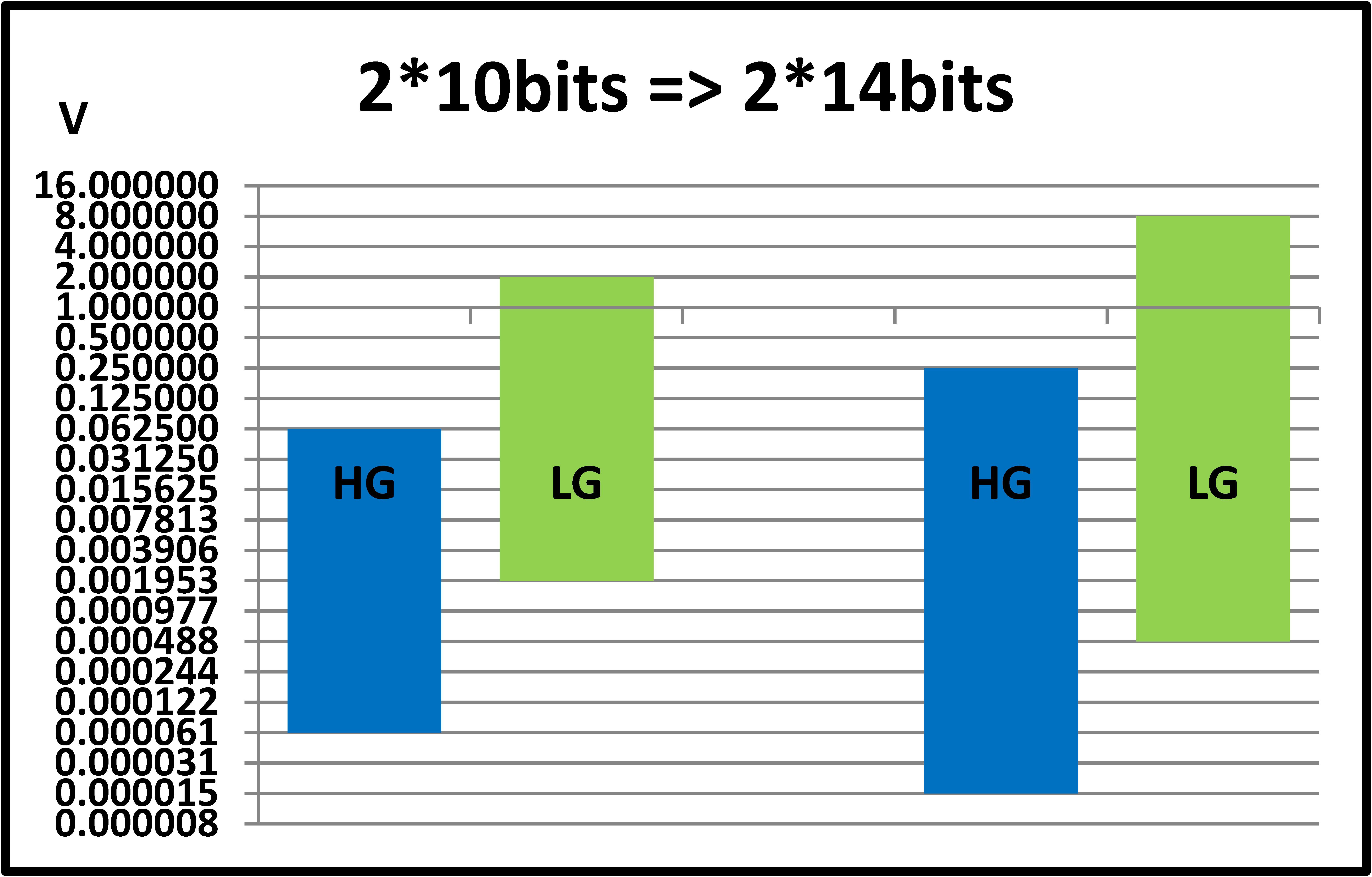
The currently used 15-bit dynamic range with two 10-bit ADCs and 5-bit overlapping is too narrow for an investigation of showers close to the core, where a saturations even in the low-gain channel appear. Front-End Board with Cyclone® V developed in the University of Łódź, as a test high-resolution platform for the Auger-Beyond-2015 Front End Electronics, contains two 14-bit ADCs per PMT (with 9-bit overlapping giving 19-bit dynamic range) and with two additional channels for potential extra sensors. For sure, 14-bit resolution in two HG and LG channels per a single PMT is not necessary in a final design. Nevertheless, a large overlapping of HG and LG channels allows a precise calibration between them for future final design optimization.
III Analog section
The ACEX/Cyclone Front-Ends use 6 identical channels driven from PMT dynodes (high-gain channels) or from PMT anodes (low-gain channels). The amplification in the HG is 32 times higher than in the LG. In the new design we are going to increase a sensitivity of measurements. Unfortunately, dynodes provide relatively noisy signals. We will use anodes only and split analog signals directly on the FEB. 14-bit ADCs in the UŁ design require a small amplification factor (only x8). Unfortunately, a total number of the LVDS receivers allows an implementation of 6*14-bit + 2*12-bit ADC. The proposed electronics upgrade provides a flexible interface to allow the other enhancements co-located with the surface detector stations to make use of the data processing and communications infrastructure of the stations.
In the new design we selected six 14-bit ADCs for 3 HG and 3 LG channels. Actually, 12-bit resolution seems to be enough. However, taking into account measurements for Auger Engineering Radio Array (AERA) we noticed a significant factor of a quantization noise.
We tested an influence of the noise on spectral characteristics short pulses typical for radio events (sine wave enveloped by a Gauss bell). Even for a noise level comparable with a level of signal the signal spectral contribution was clearly visible and easy to detect. For 3 times higher noise we observed a dramatic change of spectra practically making impossible a signal recognition. This is normal. However for higher signals (with the same signal to noise ratio) contributions for very low and very high frequencies are lower in comparison to relatively low signals, when quantization of signals additionally affect the spectra. This means that a quantization noise may be reduced in higher-resolution ADCs due to a tinier granularity [13].
Nevertheless, this is a prototype which main goal is a test of several sometimes antagonistic conditions. The final design extracts the best solutions as a compromise between the resolution, speed and the cost.
IV FPGA selection
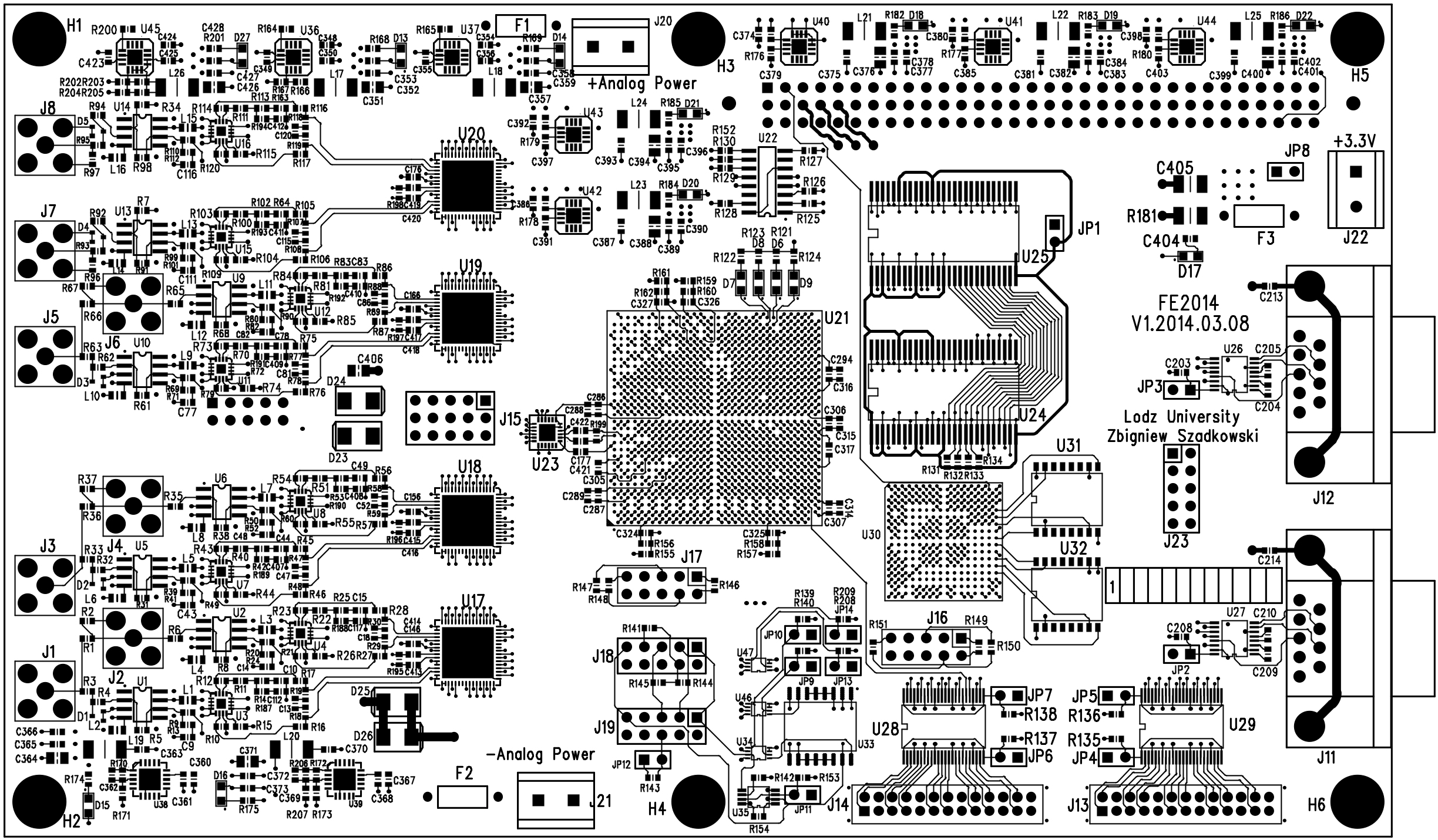
In a current design Front-End Boards are pluged-into the UB on a 96-pin connector. The University of Łódź develops an intermediate design of the still plugged-in Front-End Board with all features required for a final design: a fast sampling, a wider dynamic range, a possibility to merge other experiments.
The following criteria were crucial for the FPGA selection:
-
1.
number of LVDS receivers - to receive data from at least 8 ADCs with at least 12-bit (better 14-bit) resolution,
-
2.
an amount of equivalent logic elements (LEs) - for an implementation of a general algorithms,
-
3.
a capacity of embedded memory - for an implementation of large, fast buffers, typically as dual-port RAM,
-
4.
number of variable-precision digital signal processing (DSP) blocks that can implement 18x18 embedded multipliers - important for sophisticated algorithms like: the trigger based on the Discrete Cosine Transform (DCT) [9]-[11] for a detection of very inclined ”old” showers, the trigger based on an Artificial Neural Network (ANN) [12] for a detection of ”young” showers, potentially generated by neutrinos [4],
-
5.
number of fractional clock synthesis phase-locked loops (PLLs) - to create individual PLL clocks corresponding to each ADC LVDS clock output,
-
6.
a power consumption,
All previous generations of the FEB for surface detectors were equipped in Altera FPGAs [7][8]. However, due to a harsh competition between two large FPGA producers: Altera and Xilinx, we considered also FPGA of the 2nd one, especially the FPGA families integrating the standard fast logic with embedded micro-controllers (Hard Processing Systems - HPS) and System on Chip (SoC). Both Altera and Xilinx offer chips with HPS and SoC.
Altera’s Cyclone® V FPGAs offer the industry’s lowest system cost and power, with a high performance levels sufficient for high-volume applications. The SoC Altera Cyclone V SE family with ARM®-based HPS offers the biggest 896-pin FPGA with only 72 LVDS lines [14]. Unfortunately, it is not enough even for six 12-bit channels (we have to take into account also differential clock lines from ADCs). Other Altera’s family - Arria® V is too expensive.
The Xilinx Zynq™-7000 family provides the software programmability of a embedded processor with the hardware programmability of an FPGA. However, only a single Xilinx SoC FPGA: XC7Z100 offers a large amount of LVDS lines: 102 for FF900 package or 120 for FF1156 one [15]. This chip can support maximal nine 12-bit LVDS ADCs (with FF1156). 4 dual-channel + a single-channel 12-bit ADCs require 4*2*12+12=108 LVDS data lines + 5*2=10 lines for differential clocks.
The University of Łódź decided to use the FPGA from the Altera’s Cyclone® V E family without the SoC and HPS as not absolutely necessary for a still plugged-in FEB. The new design focuses on a reliability of the firmware (LVDS protocol with high sampling, standard and new triggers cooperations, potential lossless data compression, various modes of remote and on-side FPGA programming), optimization of the data acquisition for the final design, measurements of FEB parameters in real Argentinean pampas conditions as well as on new trigger algorithms. Additionally, all old firmware written in AHDL for ACEX, Cyclone, Cyclone III and already tested in pampas for years can be easily adjusted to the Cyclone V FPGAs. Xilinx platform, however, does not support AHDL. The firmware should be written in the VHDL or Verilog either from the scratch or should be translated from the AHDL. Experiences in a FPGA code development suggest to be very careful in simple code translation. Timing in e.g. VHDL is not the same as for the AHDL. The AHDL code translated into VHDL indicated a different timing optimization by the Quartus compiler. To keep a timing already perfectly verified in real conditions for years and to save time for additional arduous simulations for timing verification we decided to adjust the already existing AHDL code for new Cyclone V FPGAs.
Only two chips obey the above criteria : 5CEFA7 (150 kLE, 6.86 Mbit and 312 DSP 18x18 multipliers) and 5CEFA9 (301 kLE, 12.2Mbit and 684 DSP 18x18 multipliers). We decided to implement the biggest chip 5CEFA9F31I7 (industrial version with a temperature range -40∘C - +85∘C - due to large daily variation of temperature reaching even 40∘C) to keep a maximal flexibility in a development of sophisticated, resource consuming algorithms (e.g. ANN for a recognition of ”young” inclined showers).
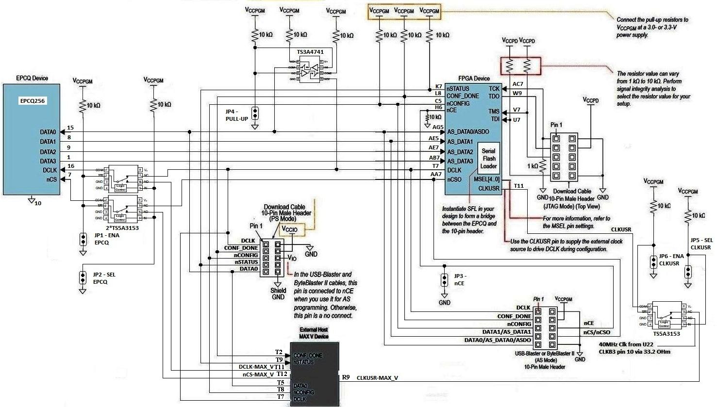
V FPGA programming
The surface detector is anticipated to be operating at least 15-20 years. In such a long period it is very likely the algorithm of the detection controlling the FPGA has to be updated. The system should be reconfigurable remotely, if possible. The currently operating FPGAs in the surface detectors can be reprogrammed via the Passive Serial mode driven from the external host - the UB. The prototype FEB based on the Cyclone® V E will be equipped in several programming modes to select the optimal one in the final version as well as to keep a redundancy in case of some modes failed.
The prototype FEB is considered as an intermediate version equipped in the very sensitive analog section (14-bit ADCs with a standard 120 MHz sampling - even 250 MHz sampling is possible) and a powerful digital trigger/memory circuitry, but plugged into the old UB (a communication via DMA at 40 MHz with 1 wait-state). This intermediate FEB will allow a verification of the new powerful system (both analog and digital sections) without a change of the existing infrastructure of the data transmission to the Central Data Acquisition Center (CDAS).
The size of the programming files for ACEX® CPLD ( generation - EP1K100Q208I7 [7]), Cyclone® ( generation - EP1C12Q240I7 [8]) or Cyclone® III ( generation - EP4C40F324I7 [10]) were on the level of 2*180kB, 150kB and 440kB, respectively. However, the size of the rbf file for the largest chip from the Cyclone® V family - 5CEFA9F31I7N (selected for the design) reaches 12MB.
The Cyclone® V E could be programmed from the UB level (as it receives the configuration file from the CDAS via radio). However, the UB contains only 2MB of RAM for a full operational system. The programming file has to be transmitted in pieces and stored in a nonvolatile memory. The transfer speed via a radio is only 2400 bps. The 12MB file will be transmitted more than 14 hours. It is too long time to be wasted only for a new file transmission. The transmission is considered in a background without a break of a normal operation. The used nonvolatile memory has a capacity 128MB, large enough to store 8 different configuration files. The prototype is equipped in several programming modes in order to increase a reliability of the entire system. All previous generation of the FEBs used only a single mode - Passive Serial, the configuration file was uploaded to the FPGA from the external host (UB). The FPGA in the current design can be programmed in a following modes:
-
1.
the Passive Serial via 10-bit connector and the USB-Blaster programmer for laboratory tests - required reprogramming after power down,
-
2.
the JTAG, considered for the laboratory tests for a temporary programming of the FPGA,
-
3.
the JTAG + Serial Flash Loader, considered for the laboratory tests, which also allows to program the configuration device EPCQ256,
-
4.
combining JTAG programming of configuration device and FPGA with Active Serial configuration of FPGA using the EPCQ256 and the USB-Blaster (the MSEL[4..0] pins cannot be driven from the digital sources, they have to be connected directly to the GND or VCC, a dynamical switch between Active and Passive Serial modes is not allowed),
-
5.
the Passive Serial (as in the previous generations of the FEBs) via the MAX V CPLD, the configuration file is uploaded sequentially from the UB to the serial NOR Flash memory N25Q00AA13GSF40F and next reloaded in a single shot from the memory to the FPGA.
-
6.
the Passive Serial via MAX V CPLD using the SDHC card (2 GB) located on the daughter board plugged into the 10-pin connector. This mode is considered as the main one for the field operation. During the SD maintenance on the field, the local staff has 30 min for a single SD, it is too short to upload several config files via standard UB serial port even with 115.2 kbps speed. UARTs in the NIOS also support max. 115.2 kbps only. The SDHC card will be programmed in the laboratory and only plugged into the connector on the pampas. A single command from the CDAS is enough to reprogram the FPGA: the command selecting the address of the config file in the SDHC card.
VI FPGA code
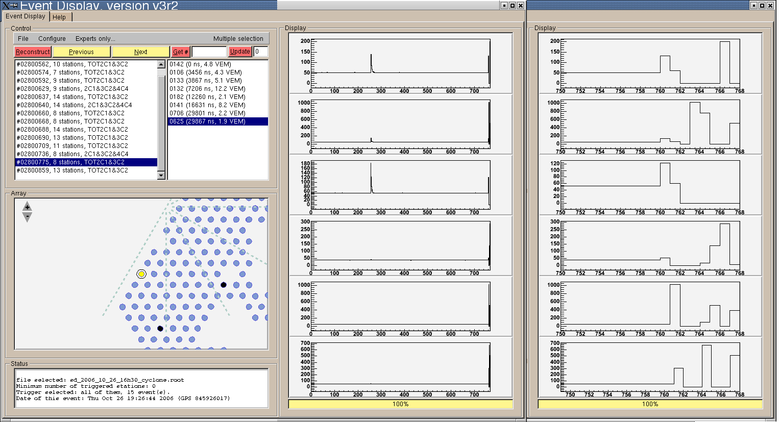
The FPGA code has been developed by the author for the APEX [16], ACEX [7], Cyclone [8] and Cyclone III [10] designs. Data from the FPGA are transferred via DMA protocol to the UB and next analyzed by the T2 software trigger via radio to the CDAS. Data are available for users in root files. Each trace for the events contains data 256 time bins before the trigger and 512 time bins after the trigger. For 40 MHz sampling frequency it takes a profile of the signals for 19.2 s. Analysis of huge amount of traces showed that last 8 words in each trace contain practically only noise. Monitoring files collect informations on the working system, however, they cannot register specific information related to the particular events. These informations have been inserted on the end of the real traces in so called ”diagnostic” mode. For one year (2010) 6 surface detectors were working with the diagnostic mode (Fig. 2) on the Engineering Array.
The currently used FEB provides 6*10 bits data for 768 time bins for each event. 60*768 matrix is a standard format for SD data. Higher resolution, higher sampling, longer traces require a new format, however, it is a task for the UUB which is currently in a development phase. This intermediate FEB has to use the standard data format in order not to change any cell in a data transmission chain.
The trigger in the surface detector array is hierarchical. Two levels of trigger (T1 and T2) are used. T2 triggers are combined with those from other detectors and examined for spatial and temporal correlations, leading to an array trigger -T3 which initiates data acquisition to the CDAS. Data for each triggered event is stored on the local UB memory for 10 s waiting for a possible T3. Two independent trigger modes are implemented as the T1, having been conceived to detect, in a complementary way, the electromagnetic and muonic components of EAS. The first T1 mode is a simple threshold trigger (Thr) which requires 3-fold coincidence above 1.75 . This trigger is used to select large signals that are not spread in time. Thr trigger is particularly effective for the detection of very inclined showers which form a flat pancake of muons and generate sharp narrow ADC traces. This trigger reduces the rate due to atmospheric muons from 3 kHz to 100 Hz. Thr trigger rate is suppressed in the T2 trigger to 20 Hz. The 2nd T1 mode - ToT (Time over Threshold) is used for a detection of particles and photons at the detector dispersed in time. ToT rate is on the level of 2 Hz and is not suppressed by the T2.
6 channels for 14-bit ADC provide 84 bit data for each time bin. 160 MHz sampling reduces the time window from 19.2 s to 4.8 s only for 768 time bins. Only HG channels participate in a trigger generation. Several configurations of data format (compatible with the standard one - not to violate the interpretation of the event by the T2, T3 and the CDAS) will be tested. All additional informations will be inserted into 8 last words of the trace (the diagnostic mode). 10 low significant bits from the 14-bit HG ADC are put on the place of standard 10 bits of the HG channel. If 14-bit value is grater than 1023 (10 LSB may be even zeros) these 10 LSB are artificially set to #3FF to inform the T2 on the saturation in the HG channel. The LG channels can contain e.g. either:
-
•
4 high significant bits of the HG ADC put on the 4 low significant bits of the LG channel + 6 most significant (but non zeros) bits from LG 14-bit ADC or
-
•
10 bits from the LG 14-bits ADC with adjusted position to neglect zeros for high significant bits if signal is small
Such a format provides non-overlapped information for strong signals as well as a possible dynamically overlapped information for relatively small signals.
4.8 s window can be too narrow especially for events registered far from the shower core which are spread on time. The FPGA stores event data in two switching buffers (to reduce a dead time) with 4 times longer length (1024 time bin before a trigger + 2048 time bin after it). The length of the buffer corresponds to 19.2 s. The additional FPGA procedure checks a signal contribution for [0..768] and [1536..3072] time bins (it means earlier than 256 time bins before the trigger and later than 512 time bins after the trigger). If a significant signal contribution were found, data can be transmitted either:
-
•
as sum of 2 or 4 neighboring time bins or
-
•
with additional 1 or 3 transmissions of ”extended” event.
| Bank | Total | Used | Voltage | Function |
|---|---|---|---|---|
| Pins | Pins | |||
| 8A | 80 | 40 | 2.5 V | 40 LVDS inputs for channels 1 - 3 |
| 7A | 80 | 40 | 2.5 V | 40 LVDS inputs for channels 3 - 6 |
| 6A | 80 | 40 | 2.5 V | 40 LVDS inputs for channels 6 - 8 |
| 5B | 48 | 36 | 1.8 V | lines controlling the ADCs at 1.8 V |
| 5A | 32 | 32 | 3.3 V | I/O data lines between FPGA and UB |
| 4A | 80 | 78 | 3.3 V | Ctrl lines (FPGA UB) + SDRAM |
| 3B | 48 | 45 | 3.3 V | Cyclone V MAX V + 2*UART |
| 3A | 32 | 31 | 3.3 V | Cyclone V MAX V |
The 1st variant provides a loss compression, the 2nd one offers lossless data transfer, however, it requires a significant software modification in the UB and the CDAS. The 2nd variant is treated as the possible backup. However, such a format modification has to be considered because data from two 12-bit ADCs (i. e. from the SPMT) should be also transmitted in a final design.
The FPGA code receives data on totally 108 (6*14+2*12) LVDS lines. Cyclone V families support OCT (On Chip Termination) option. No any external 100 resistors for LVDS termination is needed. The ADS4249 ADCs provides the outgoing clock driving the PLL in the FPGA for the optimal LVDS data receiving. 4 PLL circuits (each for double ADCs in ADS4249) with individual PLL clocks drive 3 synchronization register stages before the global FPGA clock.
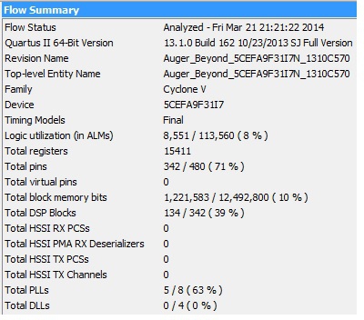
The Cyclone V FPGA implements also the NIOS processor supporting an external SDRAM (128MB), two RS232 UARTs and two 16-bit I/O buffers for additional experiments (see section III). Fig. 4 shows the compilation report for 160 MHz sampling and all 8 ADC channels with LVDS receivers, 3 DCT engines and the NIOS processor. DCT engines [11] contain sigma-delta algorithm for even huge daily temperature variation [5]. Each bank of the Cyclone V E can be supplied and drive I/O with various voltage standard. Table I lists I/O lines connected to the Cyclone V E banks.
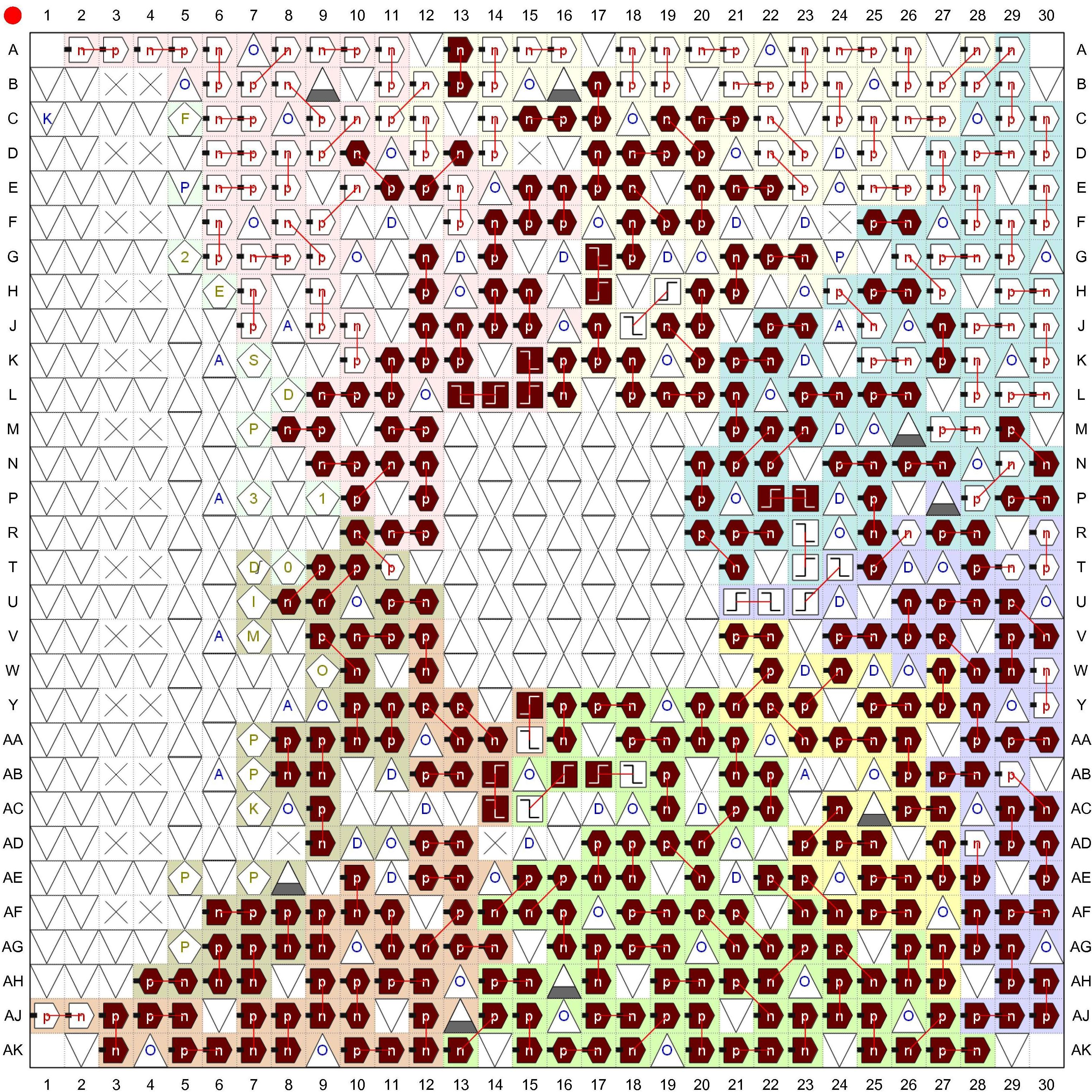
The previous version of the Quartus II v. 13.0 did not report any warnings for the FPGA code. The latest version, however, Quartus v. 13.1 reported for the previous code hundreds critical warnings due to cross-talks between LVDS and single-ended lines. The reasons was a relatively small distances between LVDS pin inputs and single-ended CMOS outputs. Movements of pin assignments with a gap of 2-3 pins removed all warnings. Nevertheless, it is a hint to select a FGPA chip with large amount of pins (e.g. BGA896 package instead of F672, U484 or U324 cheaper versions) to provide a sufficient flexibility in pins assignments (Fig. 7).
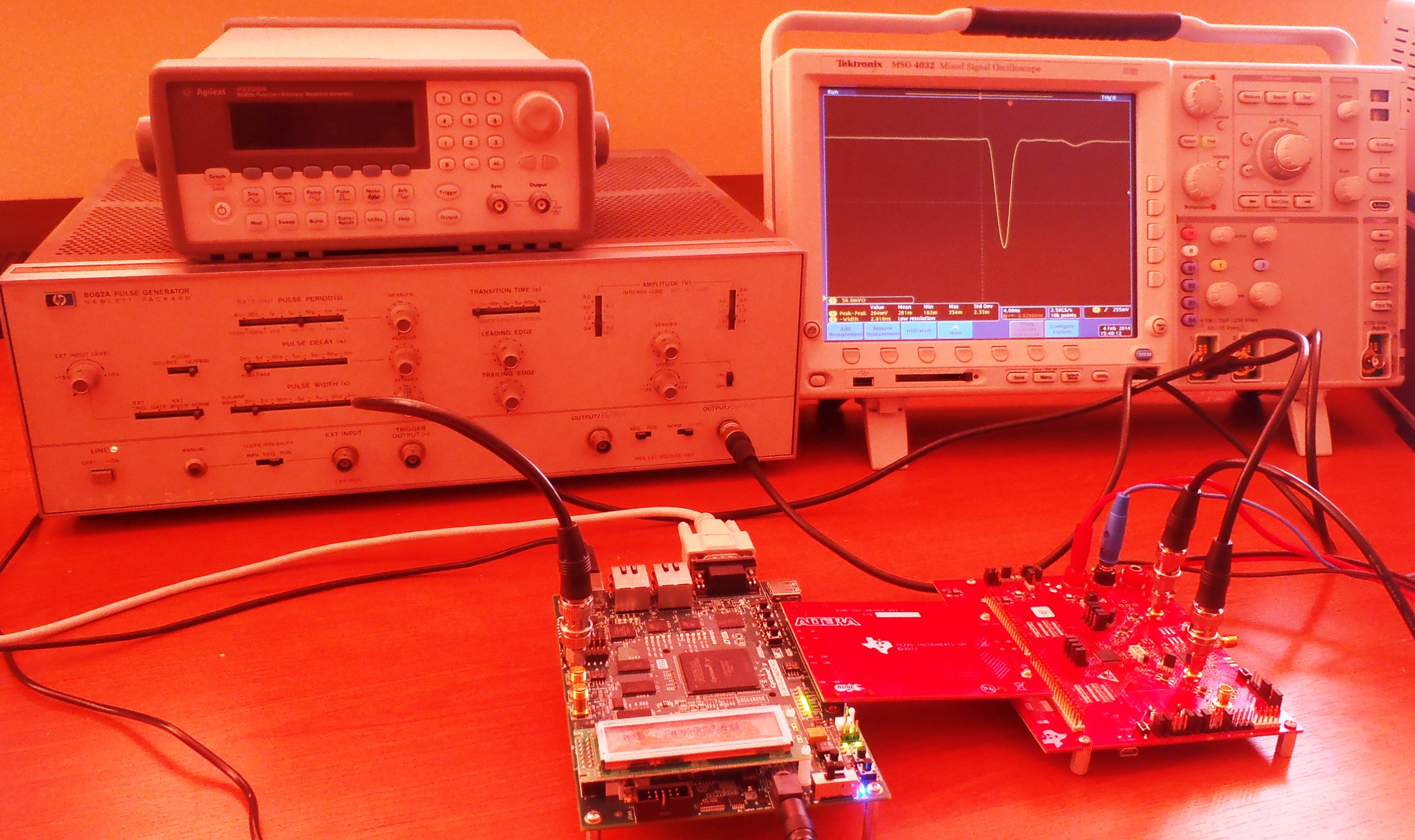
VII Design optimization in laboratory tests
The proposed sampling frequency for the new FEB is 120 MHz. However, for a prototype we developed much faster both analog electronics with a digitizer and the FPGA code. For a development we used the Altera development kit with Cyclone V E FPGA 5CEFA7F31I7. As the ADC we used Texas Instr. ADS4249EVM (Evaluation Module) with double channel 14-bit ADC with max. 250 MHz sampling. ADS4249EVM send data to the 5CEFA7F31I7 via Altera HSMC-ADC-BRIDGE in the LVDS standard. Connection between the ADC and the FPGA was a length of 20 cm and operated with very high reliability. Outgoing ADC clock supported next the internal PLL in the FPGA. Each PLL for a single ADC chip (each 2 channels) optimized reading LVDS interleaving data in a middle of a stable region. Even for 20 cm distance the LVDS transmission was perfect. In a developed FEB a distance between the ADCs and the FPGA is much shorter (Fig. 5). Input signals were tested with 200 MHz sampling.
The analog section on the ADS4249EVM contains high-frequency transformer and THS4509 differential drivers. Transformers differentiate signals and cannot be used. The differential driver does not support DC-DC connections. All serial capacitors have to be removed. DC-DC connection, however, required a significant tuning of RC components to get sharp enough rising and falling edges. Fig. 8 shows sample pulses before and after optimization. The 2 ns very short pulse (showing on the scope (Fig. 6) is read in a single time bin above a pedestal (Fig. 8).
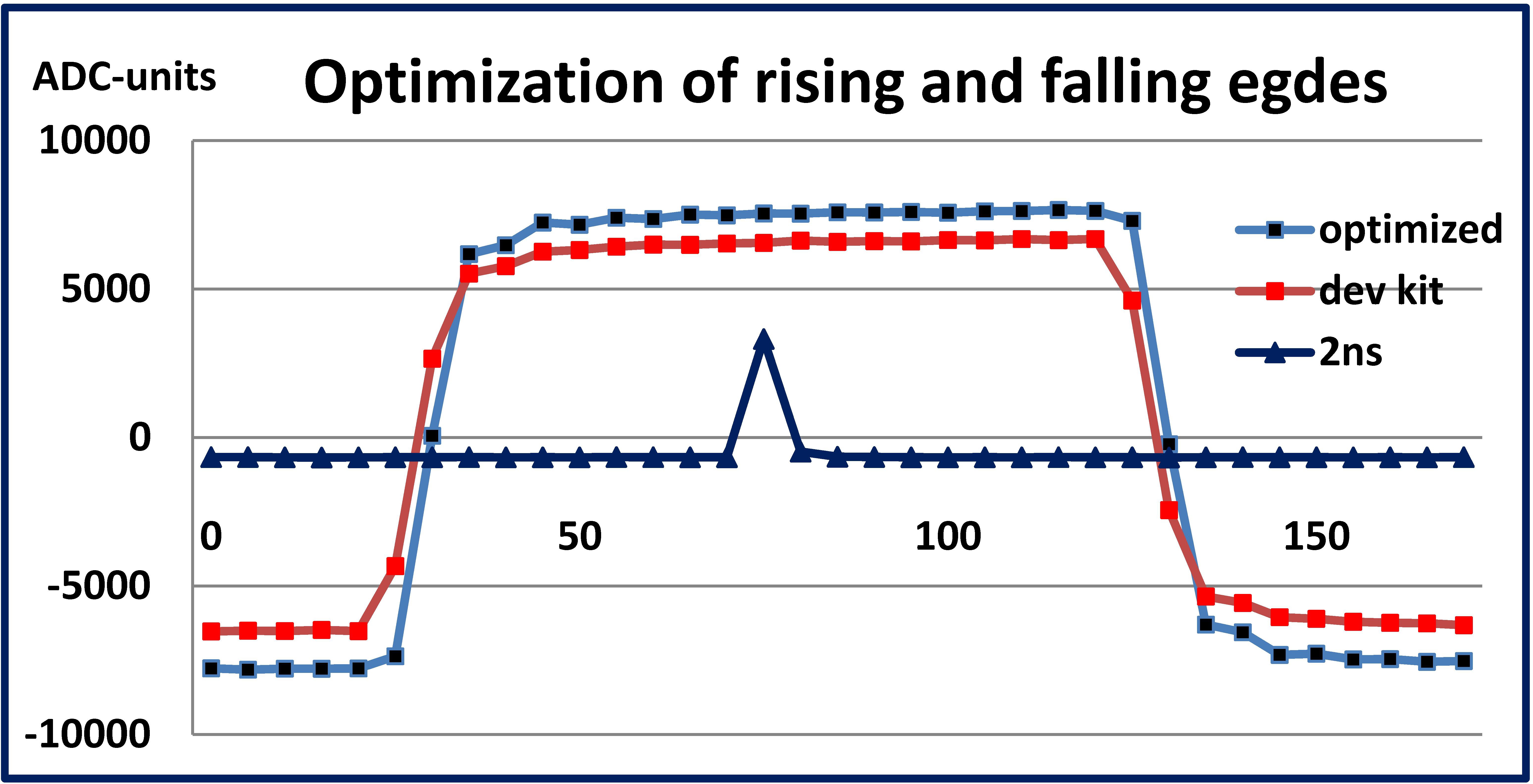
The RMS measured for long traces is on a level of 2.45 ADC-unit (14-bit data processing). Nevertheless, let us notice that the noise was measured for non-standard configuration: The ADC connected to the FPGA via ADC-HSMC-BRIDGE with two HSMC connectors (total distance 20 cm) with manually assembled resistors and capacitors for high-frequency response optimization. We expect much better final characteristics in the final FEB. The test setup, developed originally for an optimization of the upgrade design, has been used also for test of the FIR filter based on the linear predictor to suppress the RFI contaminations in the radio detectors of the AERA [17] [18] [19].
VIII Conclusion
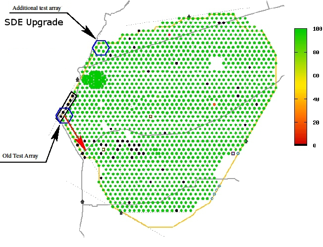
The Technical Board of the Pierre Auger Collaboration selected 8 surface detectors (hexagon + twin in the center for an investigation of possible GPS jitter) in a nord-west region of the SD array (Fig. 9) for tests of the new FEB on the Cyclone V platform with 3-4 time higher sampling and 14-bit resolution with a cooperation of the SPMT and possible other detectors. Simultaneously, the DCT triggers will be implemented parallel with the standard ones to verify the detection of very inclined showers based on an online analysis of a shape of signals in a frequency domain.
10 FEBs were ordered for a preproduction. Unfortunately, a delivery time for Cyclone V FPGA and some other components reaches 80 working days. Deployment of prototype FEBs and tests in real pampas conditions are expected in the 2nd part of 2014.
We plan tests for several months to verify 14-bit and 12-bit DAQ (2 LSBs turned-off for future cheaper 12-bit ADCs), various variants of data transmission to the CDAS in the current narrow radio channel (dynamical selection of significant range of data for lossless DAQ - both in an amplitude and a time domain or dynamical summation of neighboring time-bins for large signals, when details cease being significant), new trigger algorithms and e.g. NIOS support for temporary data storage.
We believe that data obtained from the intermediate FEBs provides a significant improvement of the final design for the Auger-Beyond-2015 which really allows new discoveries in astrophysical researches.
Acknowledgment
The author would like to thank Yury Kolotaev from the Siegen University for the PCB design.
This work was supported by the Polish National Center for Research and Development under NCBiR Grant No. ERA/NET/ASPERA/02/11 and by the National Science Centre (Poland) under NCN Grant No. 2013/08/M/ST9/00322
References
- [1] J. Abraham et al., [Pierre Auger Collaboration], “Properties and Performance of the Prototype Instrument for the Pierre Auger Observatory”, Nucl. Instr. Meth. ser. A, vol. 523, pp.50-95, May 2004.
- [2] J. Abraham et al., [Pierre Auger Collaboration], ”Trigger and aperture of the surface detector array of the Pierre Auger Observatory”, Nucl. Instr. Meth., ser. A, vol. 613, pp. 29-39, Aug. 2010.
- [3] P. Abreu et al.,[ Pierre Auger Collaboration], ”The exposure of the hybrid detector of the Pierre Auger Observatory”, Astroparticle Phys. vol. 34 Issue: 6 pp. 368-381, Jan. 2011.
- [4] P. Abreu et al.,[ Pierre Auger Collaboration], ”Search for ultrahigh energy neutrinos in highly inclined events at the Pierre Auger Observatory”, Phys. Rev. D vol. 84 Issue: 12, No: 122005, Dec. 2011.
- [5] J. Abraham et al., [Pierre Auger Collaboration], ”Atmospheric effects on extensive air showers observed with the surface detector of the Pierre Auger Observatory”, Astroparticle Phys. vol. 32 Issue: 2 pp. 89-99, Sept. 2009.
- [6] P. Abreu et al.,[ Pierre Auger Collaboration], ”Search for first harmonic modulation in the right ascension distribution of cosmic rays detected at the Pierre Auger Observatory”, Astroparticle Phys. vol. 34 Issue: 8 pp. 627-639, Mar. 2011.
- [7] Z. Szadkowski, “The concept of an ACEX® cost-effective first level surface detector trigger in the Pierre Auger Observatory”, Nucl. Instr. Meth., ser. A, vol 551, pp. 477-486, Oct. 2005.
- [8] Z. Szadkowski, K.-H. Becker, K.-H. Kampert, “Development of a new first level trigger for surface array in the Pierre Auger Observatory based on the Cyclone™ Altera® FPGA”, Nucl. Instr. Meth., ser. A, vol. 545, pp. 793-802, June 2005.
- [9] Z. Szadkowski, “A spectral 1st level FPGA trigger for detection of very inclined showers based on a 16-point Discrete Cosine Transform for the Pierre Auger Observatory”, Nucl. Instr. Meth., ser. A, vol. 606, pp. 330-343, July 2009.
- [10] Z. Szadkowski, “Trigger Board for the Auger Surface Detector with 100 MHz Sampling and Discrete Cosine Transform”, IEEE Trans. on Nucl. Science, vol. 58, pp. 1692-1700, Aug. 2011.
- [11] Z. Szadkowski, ”Optimization of the detection of very inclined showers using a spectral DCT trigger in arrays of surface detectors”, IEEE Trans. on Nucl. Science, vol. 60, no 5, pp. 3647-3653, Oct. 2013.
- [12] Z. Szadkowski, K. Pytel, ”Artificial Neural Network as a FPGA Trigger for a Detection of Very Inclined ”Young” Showers”, Contribution to the IEEE Real Time Conference, Nara (Japan), May 26-30, 2014.
- [13] Z. Szadkowski, ”FPGA Based Wavelet Trigger in Radio Detection of Cosmic Rays”, Contribution to the IEEE Real Time Conference, Nara (Japan), May 26-30, 2014.
- [14] http://www.altera.com/literature/hb/cyclone-v/cyclone5_handbook.pdf - Table 5.35
- [15] http://www.xilinx.com/support/documentation/user_guides/ug865-Zynq-7000-Pkg-Pinout.pdf - Table 1-4
- [16] Z. Szadkowski, D. Nitz, “Implementation of the first level surface detector trigger for the Pierre Auger Observatory Engineering Array”, Nucl. Instr. Meth., ser. A, vol 545, pp. 624-631, Apr. 2005.
- [17] Z. Szadkowski, E.D. Fraenkel, Ad M. van den Berg, ”FPGA/NIOS implementation of an adaptive FIR filter using linear prediction to reduce narrow-band RFI for radio detection of cosmic rays”, IEEE Trans. on Nucl. Science, vol. 60, no 5, pp. 3483-3490, Oct. 2013.
- [18] Z. Szadkowski, E.D. Fraenkel, D. Głas, R. Legumina, ”An optimization of the FPGA/NIOS adaptive FIR filter using linear prediction to reduce narrow band RFI for the next generation ground-based ultra-high energy cosmic-ray experiment”, Nucl. Instr. Meth., ser. A, vol. 732, pp. 535-539, June 2013.
- [19] Z. Szadkowski, D. Głas, C. Timmermans, T. Wijnen, ”First results from the FPGA/NIOS Adaptive FIR Filter Using Linear Prediction Implemented in the AERA Radio Stations to Reduce Narrow Band RFI for Radio Detection of Cosmic Rays”, Contribution to the IEEE Real Time Conference, Nara (Japan), May 26-30, 2014.