Interplay between the coherent and incoherent transport in quantum Hall bilayers
Abstract
We systematically study the coherent transport (Josephson tunneling and counterflow current) and its breakdown which leads to incoherent charge flow in in the excitonic BCS condensate formed in GaAs bilayers at . The Josephson currents in samples with three different interlayer distances vary by four orders of magnitude. In contrast, the breakdown thresholds for the quantum Hall state are comparable. Furthermore, Coulomb drag in a Corbino ring reveals that the coherent counterflow current coexists with the dissipative charge transport.
pacs:
73.43.-f,73.43.Lp,73.43.FjQuantum coherence is the key ingredient of many exotic states of matter. Epitomes are the superconductivity and the Bose-Einstein condensation. Interestingly, much of the physics governing the aforementioned states has been recently encountered in a quantum Hall system Yoshioka et al. (1989); Fertig (1989); Wen and Zee (1992); Girvin (2003). In a double-quantum well heterostructure, interlayer coherence emerges at a total Landau level filling of one, i.e. Spielman et al. (2000); Kellogg et al. (2004); Tutuc et al. (2004); Wiersma et al. (2004); Tiemann et al. (2008); Huang et al. (2012); Nandi et al. (2012). This spontaneous phase coherence renders the filled and vacant electronic states in the two layers into a BCS-condensate of interlayer excitons.
Experimental evidence gives strong support for the scenario of an exciton condensate. Interlayer tunneling experiments have revealed that a large dc current can be passed from one layer to the other without building up any significant voltage drop Spielman et al. (2000); Tiemann et al. (2008). Due to its resemblance to a superconductor junction, the tunneling current is therefore considered to be the interlayer Josephson current. Further developments using Corbino samples even allowed adjusting the Josephson current via the bulk exciton condensate Huang et al. (2012). The Josephson current induced on one edge shifts accordingly with a second Josephson current injected on the opposite edge. By exploiting the unique topology of a Corbino configuration, it has been established that sending charges across the annulus in one layer drags charges dissipationless in the opposite layer Tiemann et al. (2008), even in the absence of any Josephson coupling Nandi et al. (2012). This remarkable effect attests to the existence of a coherent counterflow current Su and MacDonald (2008).
Here, we enhance the coherent effects in the bilayer system by consecutively reducing the interlayer distance and study systematically the influence of interlayer distance on both the coherent processes as well as the incoherent transport. We find that the maximum Josephson current changes rapidly with the interlayer distance whereas the thresholds for the incoherent intralayer process are comparable among all bilayers investigated. Coulomb drag experiments in Corbino samples demonstrate that these incoherent intralayer processes can coexist with a coherent counter-flow current.
The wafers were grown by molecular-beam epitaxy and contain two 19 nm wide GaAs quantum wells in which the electrons reside. Symmetric doping with spacer thicknesses of about 200 nm on each side results in rather similar electron densities cm-2 and mobilities cm2/V s for the individual layers. The quantum wells are separated by alternating layers of AlAs (1.7 nm) and GaAs (0.28 nm). The three wafers contain four, five, or six AlAs/GaAs periods corresponding to about 8, 10 or 12 nm barrier thicknesses (), respectively. Separate contacts to the two quantum wells are achieved by the selective depletion technique Eisenstein et al. (1990); Rubel et al. (1998). Balanced electron densities of about cm-2 are adjusted using front and back gates. At these densities the state is reached at perpendicular magnetic fields of about 2 Tesla where the ratio becomes less than about 2. Here is the average distance between the 2DEG layers and is the magnetic length. All the measurements were carried out in a dilution refrigerator at base temperatures below 20 mK.
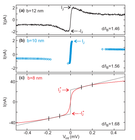
We start with the interlayer tunneling experiments which demonstrate the strong influence of interlayer distance on the coherent phenomenon. Here the source and drain contacts are placed at the two layers separately. By sweeping the bias voltage, both the interlayer current and the four-terminal interlayer voltage are recorded. Fig. 1(a)–(c) presents the current-voltage (-) characteristics from three samples with different barrier thicknesses. All three curves show a steep increase of the current around zero bias signalling the Josephson coupling between the layers. After reaching a critical current, the interlayer voltage () starts to increase rapidly. Note, that the current scales of the three plots are significantly different, while the voltage scales are the same.
Despite the overall similarity, there are significant differences in the details of the curves. For =12 nm, the - characteristic agrees very closely with theory Hyart and Rosenow (2011) and with the ones observed experimentally in devices with a similar tunneling barrier Spielman (2004). The interlayer current reaches the nA-range when the barrier thickness is reduced from 12 to 10 nm (Fig. 1(b)). Also, the - characteristics undergo a drastic change as a result of the barrier thickness reduction. Data gaps occur in regions with negative conductances and hysteresis exists in the two opposite sweep directions (data shown in Fig. 1 was obtained when sweeping upward.). Essentially, the negative differential conductance in the sample with nm causes the load line effect to become prominent. A further reduction of the barrier to =8 nm causes the interlayer - to change once more. The current is not only much larger but also the - curve is smooth again and does not show interruptions. The smoothness is generic for this type of sample with =8 nm. The same behavior has been observed on multiple samples from two wafers.
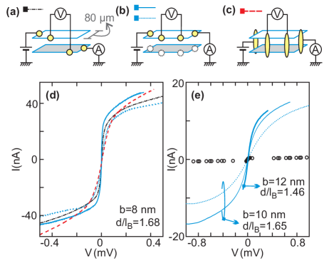
The complete disappearance of negative conductance sections in the - merits further investigation. We find that due to the strong Josephson coupling, the two layers in the sample with nm become electrically indistinguishable such that interlayer and intralayer - characteristics are identical. Note that this strong coupling only occurs at . The circuits for the interlayer and intralayer experiments on a Hall bar are sketched in panel (a) to (c) on the top of Fig. 2. Fig. 2(a) is the setup we have used for the interlayer experiment. The source and drain contacts contact the two layers separately. Furthermore, they are situated on the two opposite ends of the Hall bar. Fig. 2(b) presents a configuration where only one of the layers is exclusively selected for the measurement whereas Fig. 2(c) shows that both layers are contacted. The latter two cases reveal the intralayer transport properties.
Data obtained from the sample with 8 nm using the three configurations are shown in Fig. 2(d). Three curves marked as solid, dotted and dashed show that as soon as the in-plane current exceeds a critical current of about 20 nA the intralayer transport becomes dissipative hence the longitudinal voltage increases rapidly. This can be interpreted as a manifestation of the breakdown of the state in a way which is very similar to the breakdown of the traditional integer quantum Hall effect due to the onset of dissipative processes Nachtwei (1999). Strikingly, the - curve from the interlayer experiment (dash-dotted curve) follows closely the same breakdown behavior as the two intralayer ones. It indicates that a Josephson current of about 20 nA produces the same dissipative effect in the intralayer transport in this geometry. Larger Josephson currents are not accessible, since the dissipative intralayer process becomes important.
With larger barriers the Josephson phenomenon can be separated from the breakdown in the intralayer transport. In Fig. 2(e) at first, the interlayer (circles) and the intralayer (lines) transport of a =10 nm sample are compared. Here the critical Josephson current is about 10 times smaller than the breakdown current of the quantum Hall state. Also shown in the same panel is part of the intralayer - characteristic of the sample with a 12 nm barrier. The displayed voltage interval is limited because of a breakdown of the electrical separation of the two layers outside that range. Nevertheless, it appears that the intralayer breakdown current is in the same 10 nA range as the samples with 8 and 10 nm. In contrast to an exponential dependence on the barrier thickness followed by the interlayer Josephson currents, the breakdown currents exhibit only a weak barrier dependence.
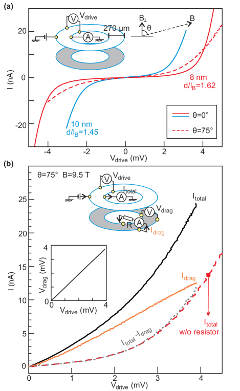
The breakdown of the state can also be observed using a Corbino geometry. The inset to Fig. 3 (a) shows the setup for a bilayer system. A (drive) voltage is applied between the outer and inner edges of the top layer. The current across the annulus is monitored as function of the interedge voltage. As the voltage increases just from zero, the current is vanishingly small. It reflects the insulating bulk property of a quantum Hall system, i.e. . Above a critical voltage the current starts to increase rapidly signaling the collapse the quantum Hall state, again in close analogy with conventional quantum Hall systems.
Exploring the same Corbino samples but under a tilted -field reveals that the same breakdown mechanism leads also to the failure of the Coulomb drag when the Josephson effect is suppressed by an in-plane magnetic field. Fig. 3 (b) displays our results from the sample with =8 nm (a sample with =10 nm showed the same behavior). A large in-plane -field is implemented by rotating the sample while keeping the perpendicular -field fixed such that . The state survives at the tilt angle of 75 degrees, but the interlayer current is below 20 pA in the interlayer voltage range -3 to 3 mV . With the interlayer current greatly suppressed, one can exclusively study the intralayer transport Nandi et al. (2012). We employ the Coulomb drag setup sketched on the top left panel of Fig. 3 (b). The directions of currents are defined by the arrows.
When no resistor is placed across the lower layer, the circuit is the same as the one presented in Fig. 3 (a). Likewise, the - characteristic shows that the current can only flow across the annulus at large bias voltages when the state breaks down (dashed curve in Fig. 3 (a)(b)). The finite conductance at small voltages is due to the weakened state under tilted -field. By bridging the outer and inner rims of the bottom layer with a resistor, currents start to flow in both layers but in opposite directions (top layer: outer to inner; bottom layer: inner to outer.). At small bias, the ratio between the drag current and the total current is close to one indicating a perfect Coulomb drag. When exceeds 2 mV, deviates from significantly— keeps increasing almost linearly whereas increases much faster. Interestingly, by subtracting the drag current from the total current, the - characteristic (dotted) collapses back to the dashed curve obtained when no resistor was mounted. It indicates that the excess current in originates from the breakdown of the state. Notably, even when the state starts to break down, the counterflow current—represented by —seems to be unaffected in the voltage range we measured (2 to 4 mV). In other words, the coherent counterflow current is still present and can flow simultaneously with the incoherent and dissipative charge current.
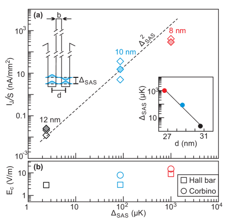
Finally, we discuss the values of the critical Josephson currents as well as those of the breakdown thresholds in the three batches of samples in Fig. 4. For samples with =12 and 10 nm, the critical Josephson currents () are well-defined (marked by the arrows in Fig. 1 (a) and (b)). For the sample with nm, we define from the crossing of a linear fit to the high voltage data ( mV) at zero bias. We use to remind that this is not the intrinsic Josephson critical current but the breakdown current of the quantum Hall state. These critical current values are normalized by the sample areas () for comparison Finck et al. (2008); Tiemann et al. (2009). They are plotted as a function of –the subband splitting that measures the single particle tunneling strength. The values of are evaluated from the interlayer conductance measured at zero -field and follow the expected exponential reduction with the interlayer distance (inset to Fig. 4 (a)). This justifies our use of as the -axis of Fig. 4. For completeness, data obtained at different ratios are also included. In general, the critical Josephson current follows the quadratic dependence on . This gives a more stringent support to the perturbation theory Hyart and Rosenow (2011) as only one parameter—the interlayer distance—is varied here. A deviation comes from samples with nm reflecting that the breakdown threshold on the intralayer transport has been reached. Fig. 4 also suggests that the largest intrinsic Josephson critical current that is not limited by the intralayer breakdown threshold will be reached at a of around 500 K.
Analyzing the breakdown behavior of the intralayer transport may shed light on the microscopic mechanism of the dissipative processes in the state. The electric Hall fields at the respective breakdowns are summarized in Fig. 4(b) for both Hall bar and Corbino samples. Their values do not differ significantly between the two sample geometries and, as already discussed, do not increase much with . They are, however, about three orders of magnitude smaller than those observed at the traditional integer quantum Hall effect Nachtwei (1999). We suggest that the breakdown at occurs when the electric Hall field is sufficient to loosen the excited quasiparticles which are vortices with charge , also called merons, that reside in puddles induced by disorder. The typical binding energy of the merons to their respective sites is about 0.1 K as deduced from the thermal activation experiments Wiersma et al. (2004). With the observed critical Hall fields ( V/m for Corbino samples) an average distance between the merons can be estimated: nm. Our estimated length is only slightly larger than the length scale (a few hundred nm) derived theoretically by Hyart and Rosenow Hyart and Rosenow (2011).
To summarize, we have shown that the Josephson coupling in the bilayer excitonic condensate state is greatly affected by the interlayer distance or by the single particle tunnel coupling constant . It is quantitatively well described by the theory of Hyart and Rosenow Hyart and Rosenow (2011). Intra layer transport shows a breakdown similar to the one observed at the integer quantum Hall effect. In the state the relevant process appears to be the loosening of merons in contrast to the inter Landau level scattering at the quantum Hall effect. The Coulomb drag experiment on a Corbino sample under tilted -field shows that the charge current of the mobile merons coexist with the excitonic counterflow current over a wide electric field range.
We acknowledge discussions with J. Smet, B. Rosenow, T. Hyart, A. H. MacDonald, P. Eastham, S. Schmult and L.Tiemann. M. Hagel assisted in the sample preparation. The experimental techniques are based upon earlier collaborations with J.G.S. Lok and L.Tiemann. This project was supported by the BMBF (German Ministry of Education and Research) Grant No 01BM900.
References
- Yoshioka et al. (1989) D. Yoshioka, A. H. MacDonald, and S. M. Girvin, Phys. Rev. B 39, 1932 (1989).
- Fertig (1989) H. A. Fertig, Phys. Rev. B 40, 1087 (1989).
- Wen and Zee (1992) X.-G. Wen and A. Zee, Phys. Rev. Lett. 69, 1811 (1992).
- Girvin (2003) S. M. Girvin, Int. Journal of Mod. Physics B 17, 4975 (2003).
- Spielman et al. (2000) I. B. Spielman, J. P. Eisenstein, L. N. Pfeiffer, and K. W. West, Phys. Rev. Lett. 84, 5808 (2000).
- Kellogg et al. (2004) M. Kellogg, J. P. Eisenstein, L. N. Pfeiffer, and K. W. West, Phys. Rev. Lett. 93, 036801 (2004).
- Tutuc et al. (2004) E. Tutuc, M. Shayegan, and D. A. Huse, Phys. Rev. Lett. 93, 036802 (2004).
- Wiersma et al. (2004) R. D. Wiersma, J. G. S. Lok, S. Kraus, W. Dietsche, K. von Klitzing, D. Schuh, M. Bichler, H.-P. Tranitz, and W. Wegscheider, Phys. Rev. Lett. 93, 266805 (2004).
- Tiemann et al. (2008) L. Tiemann, W. Dietsche, M. Hauser, and K. von Klitzing, New Journal of Physics 10, 045018 (2008).
- Huang et al. (2012) X. Huang, W. Dietsche, M. Hauser, and K. von Klitzing, Phys. Rev. Lett. 109, 156802 (2012).
- Nandi et al. (2012) D. Nandi, A. D. K. Finck, J. P. Eisenstein, L. N. Pfeiffer, and K. W. West, Nature 488, 481 (2012).
- Su and MacDonald (2008) J.-J. Su and A. H. MacDonald, Nature Physics 4, 799 (2008).
- Eisenstein et al. (1990) J. P. Eisenstein, L. N. Pfeiffer, and K. W. West, Appl. Phys. Lett. 57, 2324 (1990).
- Rubel et al. (1998) H. Rubel, A. Fischer, W. Dietsche, K. von Klitzing, and K. Eberl, Materials Science and Engineering B 51, 207 (1998).
- Hyart and Rosenow (2011) T. Hyart and B. Rosenow, Phys. Rev. B 83, 155315 (2011).
- Spielman (2004) I. B. Spielman, Ph.D. thesis, Caltech (2004).
- Finck et al. (2008) A. D. K. Finck, A. R. Champagne, J. P. Eisenstein, L. N. Pfeiffer, and K. W. West, Phys. Rev. B 78, 075302 (2008).
- Tiemann et al. (2009) L. Tiemann, Y. Yoon, W. Dietsche, K. von Klitzing, and W. Wegscheider, Phys. Rev. B 80, 165120 (2009).
- Nachtwei (1999) G. Nachtwei, Physica E 4, 79 (1999).