Reconfigurable anisotropy and functional transformations with VO2-based metamaterial electric circuits
I Abstract
We demonstrate an innovative multifunctional artificial material that combines exotic metamaterial properties and the environmentally responsive nature of phase change media. The tunable metamaterial is designed with the aid of two interwoven coordinate-transformation equations and implemented with a network of thin film resistors and vanadium dioxide (). The strong temperature dependence of electrical conductivity results in a relevant modification of the resistor network behavior, and we provide experimental evidence for a reconfigurable metamaterial electric circuit (MMEC) that not only mimics a continuous medium but is also capable of responding to thermal stimulation through dynamic variation of its spatial anisotropy. Upon external temperature change the overall effective functionality of the material switches between a “truncated-cloak” and “concentrator” for electric currents. Possible applications may include adaptive matching resistor networks, multifunctional electronic devices, and equivalent artificial materials in the magnetic domain. Additionally, the proposed technology could also be relevant for thermal management of integrated circuits.
II Introduction
Materials synthesis has reached a point where one can literally grow materials from scratch while manipulating the substance at the atomic and molecular level. This has led to various new possibilities for material properties that never existed in the past. A related field that has also seen a tremendous growth in recent years is metamaterial engineering. Artificial structures from nanoscales and up can be fabricated to collectively induce exotic properties not typically found in nature. Traditionally proposed as a platform for studying electromagnetic phenomena, metamaterials have expanded beyond the realm of optics wegener2013 ; maldovan2013 and seen applications in diverse areas including the manipulation of acoustic waves cummer2007 , magnetostatic fields narayana2012dc ; magnus2008 ; gomory2012 , heat flux narayana2012 ; narayana2013 ; schittny2013 and electric current cuiprl2012 .
In the area where the fields of material science and metamaterial engineering overlap, the ability to reconfigure the response of the materials in real time has emerged as one of the most important goals. For electromagnetic waves, the hybrid-metamaterial approach has been successful. Meta-structures with graphene papasimakis2010 , chalcogenide glass samson2010 , liquid crystals savo14 , NEMS/MEMS ou2011 , superconductors savinov2012 and vanadium dioxide (VO2) driscoll2009 ; huang2010 have for instance resulted in linear and nonlinear control of transmission characteristics, yielding frequency tunability. In contrast to these time-varying counterparts, however, the incorporation of similar hybridized structures in static (or quasi-static) electric and magnetic metamaterials has been largely unexplored to date. Because of their intrinsically non-resonant nature, it is clear that a reconfigurable frequency response would not be the aim, but a more drastic operational shift may be feasible from a functional device made of DC hybrid-metamaterials.
In this manuscript we report the experimental integration of VO2 phase change materials in DC electric metamaterial structures. We have designed a metamaterial electric circuit (MMEC) with cloaking-like and concentrating-like functionalities with the aid of a coordinate-transformation method theory pendry2006 . We have then implemented the MMEC on a 4-inch silicon wafer using thin film technology and circuit theory. The material switches by itself from one functionality to the other via VO2 metal-to-insulator transitions induced by an external temperature change. The experimental results and the theoretical approach presented here demonstrate the concept of embedding functional substances in bigger artificial heterostructures to induce another level of functionalities, while pointing the way toward analogous investigations and potential applications in a multitude of electrical, magnetic, and thermal systems.
III Results
We begin by viewing the material to be constructed as a system consisting of an ensemble of elements that collectively give rise to the material’s overall characteristics. This conceptual transition from a continuous medium to an equivalent discretized version provides a powerful tool for designing the anisotropic properties of artificial materials and introduces a functional component better suited for practical implementations cuiprl2012 ; dede2013 . In this particular case, we mimic a continuous cylindrical conducting medium of conductivity and thickness using a polar resistor network comprising of spokes and arcs of finite lengths and , where and denote the radial and angular directions in cylindrical coordinates. The dimensions of spokes and arcs can be calculated from Ohm’s law, and . By properly assigning the dimensions and conductivities of the polar grid elements, it is possible to mimic the properties of any continuous medium and hence achieve unprecedented control over the electric current flowing through the material.
Needless to say, the resistive network topology itself is relevant for many circuit applications including filters zobel23 ; norton37 , matching networks for power electronics han07 and electric impedance tomography (EIT) borcea08 ; cheney1999 . Design strategies include minimization of power dissipation roos2012 , resistance distance klein93 , and dealing with inverse problems borcea08 . The choice strongly depends on the desired application. In this work we apply the resistive network to mimic a continuous medium while gaining control over the spatial anisotropy.
In tailoring spatial anisotropy for DC metamaterials, all previous works have focused on single functionalities (e.g. cloak, concentrator) cuiprl2012 ; cuiscirep2012 ; cuiapl2013 or made use of additional DC sources for altering the spatial distribution of electric currents cuiprl2013 . For realistic applications the ability of a metamaterial electric (and eventually electronic) circuits to readily respond to the surrounding environmental variations (e.g. temperature changes) is of strategic importance. Combining metamaterials with environmentally responsive material compounds could pave the way for such multifunctional metamaterial electric circuits.
The material discretization is followed by the assignment of resistance values for all constitutive elements. The multifunctional scenario considered here naturally requires two sets of such values with a way to switch between the two. To demonstrate reconfigurability, we have picked the examples of cloaking-like and concentrator-like functionalities for the two electric properties of the overall material, and we employ VO2 as the temperature dependent switch. We first utilize the concept of coordinate-transformation to determine the spatial resistance profiles for the two scenarios. Such coordinate-transformation-based designs have the exclusive advantage of being naturally impedance matched pendry2006 ; schurig2006 ; leonhardt2006 , and for this reason the load variation arising from spatial resistance change will not be sensed by the external circuitry and sources. Furthermore, with regard to applications, designs based on coordinate-transformation could be employed to guarantee robustness against natural fluctuations of circuit parameters.
We refer readers to the appendix section for the details of the coordinate-transformation formalism. We note briefly here that, as the first type of anisotropic material, we induce the so-called “truncated cloak”. A well-established ruan2007 coordinate transformation of is used to compress space from a cylindrical region into an annular region (see appendix A). As , all electrical current would be removed from the core region . For the second type of anisotropy, we induce a “concentrator”. For this case, instead of standard coordinate transformations used in the past cuiscirep2012 , we introduce a new transformation where . This new formalism effectively links the two transformations and makes the practical design for multifunctionality feasible. We plot in Fig. 1b the radial and angular components of the polar network resistance Rρ and Rϕ, obtained from the coordinate-transformation framework above for the two functionalities.
When Rρ=R (orange continuous line), the overall material mimicked by the resistor grid functions as a truncated cloak. A perfect cloak would require infinite conductivity at the core boundary, making it prohibitive to simultaneously implement the anisotropy required for the concentrating behavior. For this reason we induce a truncated cloak as discussed above thereby allowing only a small fraction of the current to penetrate the inner region while ensuring that the electrical current profile is not perturbed in the exterior region (). When Rρ=R (blue dashed line) the current is forced to flow into the core region, while the current profile remains the same in the exterior as the cloaking scenario. The degree of concentration depends nonlinearly on the geometric factors and .
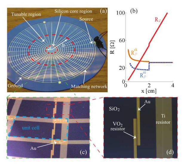
In Figure 1a, we show a camera image of our MMEC fabricated on a 4-inch silicon wafer. The resistance profiles R and Rϕ are implemented by patterning titanium (Ti, ) rectangles with fixed length () and thickness () and variable width to match the desired resistance values at particular locations. To reconfigure the anisotropy of the overall material mimicked by the network, VO2 thin film resistors have been grown in parallel with the Ti resistors oriented radially. The three orders of magnitude reduction in the VO2 electric resistivity across the phase transition allows us to approximately match the lower radial resistance of R required. Figures 1c and 1d show closeups of the MMEC unit cells and the thin film patterns, respectively. Electrical links between resistors are guaranteed by rectangular Au pads positioned at every node. The center of the grid is left open and is electrically connected to the silicon wafer forming a core region with radius and thickness . The rest of the silicon wafer surface is made insulating with a layer of silicon dioxide. The dimensions, and hence resistances, of all the thin film elements on SiO2 surrounding the core are obtained through coordinate-transformations with the core silicon () as the “background medium” taking its thickness into account to appropriately impedance-match it. Moreover the outermost circle acts as the ground and it is connected to the rest of the circuit through matching resistors made of tantalum nitride (TaN, ) to emulate an infinite material. Overall the network consists of a polar array of thin film resistors and a array of VO2 elements. Details on the calculations regarding the thin films and matching resistors, dimensions and resistances of Au, Ti, TaNi, and VO2 films, as well as detailed fabrication/growth steps are listed in the appendix C.
The characterization of the metamaterial electric circuit is carried out by mapping the voltage spatial distribution over the polar grid by probing the voltage at every node. The MMEC is fed with a DC power supply (HP 3611A) connected to the node from the center of the polar grid (see fig. 1a). The voltage amplitude is measured with respect to the ground. A custom made probe station with three motorized linear axes is used to sense the voltage at each node. Two stepper motors are programmed to position the sample horizontally, whereas the third stepper motor moves a spring-loaded contact probe vertically. The electric signal is measured with a HP34401A multimeter. In order to induce the desired change of the VO2 resistivity the sample was mounted on an electronically controlled hot chuck.
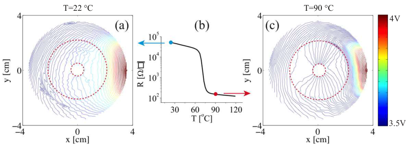
Figure 2a and 2c show the voltage maps measured at room temperature of and at , respectively. The region within the two red dashed circles is the tunable region. In fig. 2b we also plot the VO2 sheet resistance as a function of the temperature. The metal-insulator transition for the VO2 used in this experiment was designed to take place between and . The measured voltage contour maps are markedly different at the two operating temperatures. The voltage distribution at T= shows the typical signature of a truncated cloak ruan2007 , where external equipotential contour lines distribute almost undisturbed as if the tunable metamaterial region did not exist. Only in proximity of the outermost red dashed circle the equipotential lines show some perturbation. This is in agreement with the coordinate-transformation equations used for the design of our MMEC (see appendix A). At T= the profile changes drastically (see Figure 2c) as a result of the VO2 insulator-to-metal transition and shows a voltage distribution characteristic of a concentrator. The contour lines are pulled towards the core region while the exterior region shows minimum perturbation. Under this condition the VO2 behaves as a conductor and the equivalent resistance of the radial branches is significantly lower.
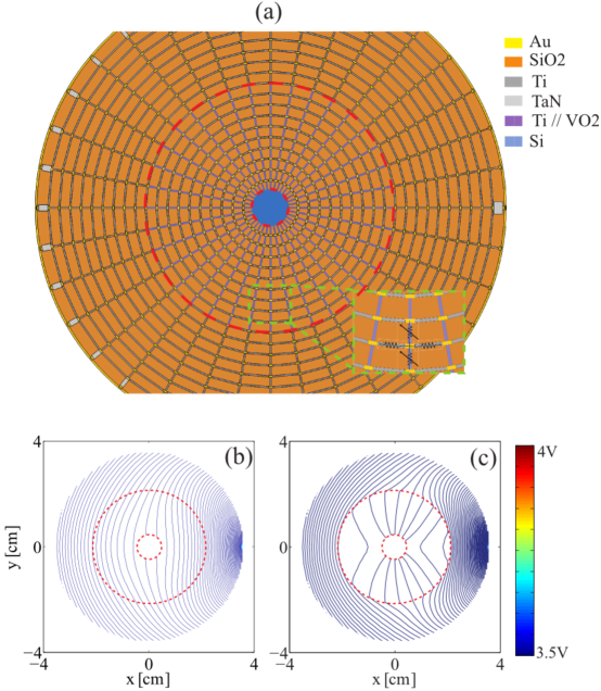
Our experimental results are confirmed by finite-element numerical simulations performed via the commercial software package COMSOL comsol . Figure 3a shows a color coded schematics of the 2D model used to simulate the MMEC. Each color refers to a different material used to implement the model. The reader can refer to the appendix C for the electric conductivity values used to describe the model. The conductivity of the silicon inner region is made 2500 times larger in this 2D simulation in order to account for the thickness difference between the conductive thin films forming the polar grid and the silicon core which is thick. The resistors Rρ are modeled through resistive elements having the same pattern as the titanium thin films. The transition from R to R is obtained by changing the conductivity of purple elements located inside the tunable region, enclosed between the two concentric red dashed circles (see inset Figure 3a). The truncated-cloaking and concentrator functionalities measured experimentally are matched well by the numerical simulations when the conductivity of the purple spokes is varied by a factor of 14. Based on our experimental implementation of Au/VO2 bridges in parallel with Ti, we expect the resistance in the radial direction to change by a factor of 18 at the VO2 phase transition. The two corresponding maps with the numerical results are shown in Figure 3b and Figure 3c.
The amplitude differences between the experimental and numerical contour maps are primarily caused by the conductivities of the TaN matching resistors next to the grounding circle. TaN is deposited by means of sputtering, and its final conductivity is strongly dependent on the N2 flow rate. We have found that this dependence is highly nonlinear especially in proximity of the target values, making it nontrivial to meet the exact conductivity values required. Subsequent tests of the TaN resistivity values have confirmed a two fold difference with respect to the expected values. The present design is very demanding in terms of fabrication tolerances because the differences between the dimensions of neighboring resistors are small, ranging between and . Typical tolerances of the contact aligner () for example could affect the above dimensions enough to cause noticeable fluctuations in the voltage profiles. This was made even more challenging as the MMEC required patterning of very small features over a large surface. The turbulent profile of some of the contour lines may be related to this non-uniformity of thin film resistors across the entire 4-inch wafer. Despite the aforementioned matters, the experimental results clearly demonstrate the reconfigurable anisotropy of the metamaterial.
The experimental results reported in this manuscript suggest that the metamaterial paradigm may be used to provide solutions for tangible compact electronics using thin film technologies. Traditionally, electronic systems comprise of several blocks, each designed to play a specific role. A smarter design approach could rely on a single unit capable of handling multiple functions such as carrying electric current and heat simultaneously but independently. A potential first step in this direction has been shown recently using metamaterial structures designed with the framework of multiphysics transformations moccia2013 . The same goal may be approached through a different path of utilizing phase change materials that have varying responses in different physical domains.
For example it has been shown that VO2 exhibits a change in its thermal conductivity upon phase transition, but it is dwarfed by the variation in its electrical conductivity andreev1978 ; chen2012 ; oh2010 . This asymmetry in the two physical domains may be utilized to obtain two independent functionalities for heat and electricity. One can imagine adding right on top of a MMEC an additional network of material (such as BeO2) with high thermal conductivity and limited electrical conductivity. When the metal-to-insulator transition takes place, only the electrical current profile within the overall material would be reconfigured, leaving the heat flux distribution unchanged. It is also conceivable to design layers to reconfigure both kinds of transport simultaneously but in different fashions. This line of bilayer approach, which takes advantage of nonlinear phase change materials with strongly different electrical and thermal properties, may be useful for designing more compact electronic components with nontrivial multifunctionalities. We note in relation to this that recently a beautiful experimental work has been reported where thin film technology combined with coordinate-transformation approach are used to fabricate systems for the unconventional manipulation of heat flux using the discretization of thermal conductors to introduce anisotropy dede2013 . Potential applications include thermal management of integrated circuits such as responding to temperature changes and rerouting electrical current away from hot spots while reconfiguring its path in a prescribed and pseudo-automated fashion.
IV Conclusions
In conclusion, this work presents the development and characterization of a reconfigurable metamaterial electric circuit, designed to respond to temperature changes through dynamic variation in its spatial anisotropy. The tunable metamaterial device is built by combining a network of thin film resistors and vanadium dioxide (VO2). The strong temperature dependence of the VO2 electrical conductivity results in a significant modification of the resistor network behavior, giving rise to a new level of functionalities. Through a new set of coordinate-transformation equations, used to tailor the response of the metamaterial circuit upon temperature change, we have shown that our MMEC mimicking a continuous and anisotropic medium can act as a truncated cloak or concentrator for electric currents. When designing an electronic system, the influence of the surrounding environment can be considered either a nuisance and hence something to be suppressed or a convenient knob that can be turned to affect the material properties. In the latter view, an ideal scenario would be to have the system designed in such a way that the external effect could be amplified and not only the local material characteristics but also the collective device property can be drastically manipulated with environmental stimuli. For such device designs and fabrications, a new paradigm could appear from the marriage of environmentally responsive materials - phase change materials - and the framework of metamaterials tailored with the mathematical formalism of coordinate-transformation.
V Acknowledgments
S. S. and Y. S. acknowledge support from the Rowland Institute at Harvard University. S.R. acknowledge NSF for financial support.
VI Appendix A: Coordinate-Transformation Method
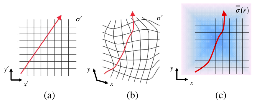
We start considering an auxiliary space filled with an isotropic material with electrical conductivity [cf. Figure 4(a)]. At equilibrium, the sourceless electrical conduction equation is given by
| (1) |
with denoting the electrical potential. Assuming, for instance, a homogeneous conductivity distribution , and applying a constant voltage along a given direction, the electrical current density follows a straight path. Next, we apply a coordinate transformation,
| (2) |
to a curved-coordinate space , which modifies the path of the electrical current density in a desired fashion [cf. Figure 4(b)]. In view of the co-variance properties of equation (1), the transformation induced in the electric potential in this new space pendry2006 ,
| (3) |
can be equivalently obtained in a flat Cartesian space filled with an inhomogeneous, anisotropic “transformation medium” [cf. Figure 4(c)] characterized by a conductivity tensor pendry2006
| (4) |
where
| (5) |
is the Jacobian matrix associated with the coordinate transformation in equation (2), and the superscripts “-1” and “-T” denote the inverse and inverse-transpose, respectively.
In particular, by considering a radial transformation,
| (6) |
between the associated cylindrical systems () and (), the relevant components of the conductivity tensor in equation (4) can be written as
| (7) |
with the overdot denoting differentiation with respect to the argument.
In our study, we are interested in switching between two functionalities induced by different coordinate transformations. More specifically, we consider an “invisibility-cloak” functionality induced by the coordinate transformation
| (8) |
and a “concentrator” functionality induced by the coordinate transformation
| (9) |
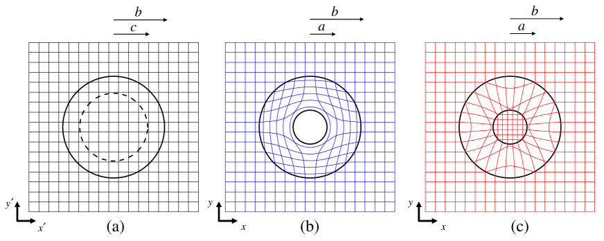
As illustrated in Figure 5, for small values of , the above cloak and concentrator transformations essentially map an annular cylinder of radii and in the transformed space onto a cylinder of radius and an annular cylinder of radii and , respectively, in the auxiliary space . Figure 5 also illustrates the coordinate distortions induced by these two transformations.
We highlight that the transformations in equations (8) and (9) are intertwined, and they are slightly different from the ones conventionally used in the literature cuiprl2012 ; rahm . In particular, the transformation in equation (8) actually yields an imperfect cloaking effect (with the ideal case recovered in the limit ), while the transformation in equation (9) is purposely chosen so as to simplify the subsequent implementation.
Via straightforward application of equation (7), we can analytically derive the expressions of the conductivity profiles associated with the two transformations. More specifically, for the cloak functionality, we obtain
| (10) |
from which we observe that the approximate character of the transformation in equation (8), for finite values of , prevents the arising conductivity components to exhibit extreme values at the inner boundary , viz.,
| (11) |
As a consequence, an imperfect cloaking effect is attained, with the electrical current density inside the inner region not exactly vanishing, but reduced by a factor proportional to
| (12) |
On the other hand, for the concentrator functionality, we obtain
| (13) |
In this case, the electrical current density inside the inner region is enhanced by a factor
| (14) |
The parameters and can be computed from equation (12) and (14), once the desired cloaking and concentration factors and have been set. In our design, we chose and .
We note from equations (11) and (13) that the aforementioned intertwining of the two transformations yields, for the two functionalities, conductivity components that differ only by multiplicative constants. This significantly simplifies the subsequent implementation, based on a polar resistor network comprising of spokes and arcs of finite lengths and , respectively, and thickness . The resistance profiles and in this network are readily related to the conductivity profiles via Ohm’s law cuiprl2012 ,
| (15) |
From equation (15), it is evident that the switching between the cloak and concentrator functionalities requires the reconfiguration of both resistance profiles and . However, in our proposed design, we followed a simplified approach by assuming
| (16) |
so that only the radial resistance profile need to be reconfigured. In order to better understand the approximation underlying this assumption, it is insightful to look at the conductivity profiles generated by assuming that the cloak and concentrator transformations are applied to auxiliary spaces with different background conductivities and , respectively, viz.,
| (17) |
| (18) |
We note from equation (15) that the simplifying assumption in equation(16) implies
| (19) |
which can be achieved from equation (18) by assuming
| (20) |
and also yields
| (21) |
We observe from equation (21) that, in view of the judicious intertwining of the two transformations, the reconfiguration required on the radial resistance profile amounts only to a constant scaling factor.
The above interpretation, in terms of cloak and concentrator transformations applied to two different and properly chosen auxiliary spaces, inherently implies that it is no longer possible to achieve perfect impedance matching for both functionalities. In our proposed design, we chose to enforce the perfect impedance matching for the cloak functionality, thereby allowing a moderate mismatch on the concentrator side.
VII Appendix B: Deposition Method
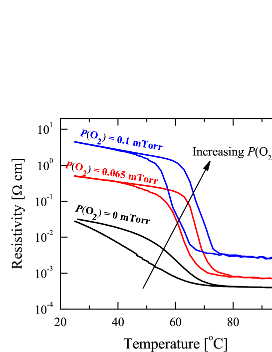
thin films were grown on 100 nm thick thermal on Si wafer by RF magnetron sputtering from a target in an gas mixture. The growth temperature and total pressure were kept constant at and 5 mTorr during the deposition, respectively. It is known that the resistivity and the metal-insulator transition temperature of are extremely sensitive to any subtle change in the oxygen partial pressure during the growth. As a result, the oxygen partial pressure was carefully controlled by adjusting the relative flow rate of pure Ar and that of balance Ar, which allows us to tune the oxygen partial pressure down to 0.02 mTorr when the total pressure is fixed at 5 mTorr. Figure 6 shows the resistivity-temperature curves of samples grown under different oxygen partial pressure. The resistivity was measured by 4-probe Van der Pauw measurements on a temperature-controlled hot chuck. The thickness of the films and therefore growth rate were calibrated by X-ray reflectivity and optical ellipsometry. The resistivity of in both the insulating and metallic phases decreases with decreasing oxygen partial pressure, because of the extra free electrons donated by oxygen vacancies formed during the growth. When the oxygen partial pressure is zero, both the metal-insulator transition magnitude and temperature are suppressed by oxygen vacancy formation. On the other hand, if the oxygen partial pressure exceeds 0.1 mTorr, the deposited films are further oxidized into that does not exhibit any metal-insulator transitions (not shown). As a result, in order to achieve large on/off ratio and have reasonable device dimensions, for the present work we chose the resistivity-temperature curve of samples grown under oxygen partial pressure of 0.065 mTorr.
VIII Appendix C: Device Parameters
The MMEC design comprises of two steps. During the first step we calculate the resistance values and from equation (15). To validate our design we run numerical simulations of the polar grid network using COMSOL. For the device fabricated experimentally with thin film technologies, different resistance values are achieved by using materials of fixed conductivities but varying the dimensions of relevant spokes and arcs making up the discretized grid. For numerical simulations, to simplify the computation, spokes and arcs of fixed dimensions are used while varying their electrical conductivities in order to match the desired anisotropic profile obtained from equation (15). The second design step involves the calculation of the dimensions of the polar grid for the real device. Table 1 lists the values of and of the thin film resistors used in our experiment and the corresponding values for their widths. Lengths and angular dimensions are fixed and their values are and . Resistors have been fabricated with Titanium films () and the film thickness is fixed at .
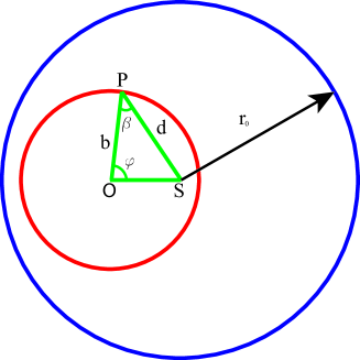
In table 1 are also listed the resistances and widths of the matching network. The values are derived from
| (22) |
to emulate an infinite medium cuiprl2012 . In Figure 7 are shown all the variables of the last equation. In particular is the distance between the ground and the source point S, is the conductivity of the background medium (), and . resistors are made with TaN (). The values are calculated through Ohm’s law where we fix the radial length () and the thickness (). Although for our experiment we utilize the central core region of a Silicon wafer () as the “background medium”, we set here. This allows us to design the surrounding material (emulated by the network grid) that is slightly more conducting than the core medium, which ensures stronger cloaking properties.
In Table 2 are listed the resistance values and of the in the insulating () and conductive state (). Through Ohm’s law we calculate the corresponding widths of the resistors . Also for these resistors we have fixed the lengths () and thicknesses ().
| n | ||||
|---|---|---|---|---|
| 1 | 39.26 | 3.79 | 217.93 | 228.11 |
| 2 | 33.75 | 8.80 | 253.47 | 314.72 |
| 3 | 31.77 | 13.99 | 269.31 | 334.11 |
| 4 | 30.73 | 19.28 | 278.36 | 341.17 |
| 5 | 30.10 | 24.61 | 284.19 | 344.70 |
| 6 | 29.68 | 29.93 | 288.24 | 347.11 |
| 7 | 29.37 | 35.29 | 291.24 | 348.38 |
| 8 | 29.14 | 40.66 | 293.55 | 349.25 |
| 9 | 28.96 | 46.00 | 295.36 | 350.11 |
| 10 | 28.82 | 51.37 | 296.85 | 350.56 |
| 11 | 27.50 | 59.24 | 311.09 | 336.19 |
| 12 | 27.50 | 64.62 | 311.09 | 337.67 |
| 13 | 27.50 | 70.00 | 311.09 | 338.92 |
| 14 | 27.50 | 75.38 | 311.09 | 340.00 |
| 15 | 27.50 | 80.76 | 311.09 | 340.93 |
| 16 | 27.50 | 86.14 | 311.09 | 341.75 |
| 17 | 27.50 | 91.53 | 311.09 | 342.47 |
| 18 | 27.50 | 96.91 | 311.09 | 343.11 |
| 19 | 27.50 | 102.29 | 311.09 | 343.68 |
| n | n | ||||
|---|---|---|---|---|---|
| 1 | 100.30 | 2313.13 | 20 | 100.30 | 2313.13 |
| 2 | 1032.63 | 224.67 | 21 | 1032.63 | 224.67 |
| 3 | 1580.63 | 146.78 | 22 | 1580.63 | 146.78 |
| 4 | 1577.18 | 147.10 | 23 | 1577.18 | 147.10 |
| 5 | 1416.57 | 163.78 | 24 | 1416.57 | 163.78 |
| 6 | 1231.04 | 188.46 | 25 | 1231.04 | 188.46 |
| 7 | 1056.33 | 219.63 | 26 | 1056.33 | 219.63 |
| 8 | 900.91 | 257.52 | 27 | 900.91 | 257.52 |
| 9 | 765.49 | 303.08 | 28 | 765.49 | 303.08 |
| 10 | 648.67 | 357.66 | 29 | 648.67 | 357.66 |
| 11 | 548.68 | 422.84 | 30 | 548.68 | 422.84 |
| 12 | 463.85 | 500.16 | 31 | 463.85 | 500.16 |
| 13 | 392.78 | 590.66 | 32 | 392.78 | 590.66 |
| 14 | 334.34 | 693.90 | 33 | 334.34 | 693.90 |
| 15 | 287.63 | 806.59 | 34 | 287.63 | 806.59 |
| 16 | 251.96 | 920.78 | 35 | 251.96 | 920.78 |
| 17 | 226.83 | 1022.81 | 36 | 226.83 | 1022.81 |
| 18 | 211.88 | 1094.97 | 37 | 211.88 | 1094.97 |
| 19 | 206.92 | 1121.22 |
| n | |||
|---|---|---|---|
| 1 | 715.29 | 2.15 | 1615.23 |
| 2 | 614.99 | 1.85 | 1878.64 |
| 3 | 578.81 | 1.74 | 1996.10 |
| 4 | 559.99 | 1.69 | 2063.18 |
| 5 | 548.50 | 1.65 | 2106.38 |
| 6 | 540.80 | 1.63 | 2136.37 |
| 7 | 535.23 | 1.61 | 2158.63 |
| 8 | 531.02 | 1.60 | 2175.71 |
| 9 | 527.76 | 1.59 | 2189.18 |
| 10 | 525.12 | 1.58 | 2200.17 |
References
- (1) M. Wegener, “Metamaterials beyond optics,” Science, vol. 342, no. 6161, pp. 939–940, 2013.
- (2) M. Maldovan, “Sound and heat revolutions in phononics,” Nature, vol. 503, no. 7475, pp. 209–217, 2013.
- (3) S. A. Cummer and D. Schurig, “One path to acoustic cloaking,” New Journal of Physics, vol. 9, no. 3, p. 45, 2007.
- (4) S. Narayana and Y. Sato, “Dc magnetic cloak,” Advanced Materials, vol. 24, no. 1, pp. 71–74, 2012.
- (5) F. Magnus, B. Wood, J. Moore, K. Morrison, G. Perkins, J. Fyson, M. Wiltshire, D. Caplin, L. Cohen, and J. Pendry, “A dc magnetic metamaterial,” Nature materials, vol. 7, no. 4, pp. 295–297, 2008.
- (6) F. Gömöry, M. Solovyov, J. Šouc, C. Navau, J. Prat-Camps, and A. Sanchez, “Experimental realization of a magnetic cloak,” Science, vol. 335, no. 6075, pp. 1466–1468, 2012.
- (7) S. Narayana and Y. Sato, “Heat flux manipulation with engineered thermal materials,” Physical review letters, vol. 108, no. 21, p. 214303, 2012.
- (8) S. Narayana, S. Savo, and Y. Sato, “Transient heat flux shielding using thermal metamaterials,” Applied Physics Letters, vol. 102, no. 20, p. 201904, 2013.
- (9) R. Schittny, M. Kadic, S. Guenneau, and M. Wegener, “Experiments on transformation thermodynamics: molding the flow of heat,” Physical review letters, vol. 110, no. 19, p. 195901, 2013.
- (10) F. Yang, Z. L. Mei, T. Y. Jin, and T. J. Cui, “dc electric invisibility cloak,” Phys. Rev. Lett., vol. 109, p. 053902, Aug 2012.
- (11) N. Papasimakis, Z. Luo, Z. X. Shen, F. De Angelis, E. Di Fabrizio, A. E. Nikolaenko, and N. I. Zheludev, “Graphene in a photonic metamaterial,” Optics express, vol. 18, no. 8, pp. 8353–8359, 2010.
- (12) Z. Samson, K. MacDonald, F. De Angelis, B. Gholipour, K. Knight, C. Huang, E. Di Fabrizio, D. Hewak, and N. Zheludev, “Metamaterial electro-optic switch of nanoscale thickness,” Applied Physics Letters, vol. 96, no. 14, p. 143105, 2010.
- (13) S. Savo, D. Shrekenhamer, and W. J. Padilla, “Liquid crystal metamaterial absorber spatial light modulator for thz applications,” Advanced Optical Materials, vol. 2, no. 3, pp. 275–279, 2014.
- (14) J.-Y. Ou, E. Plum, L. Jiang, and N. I. Zheludev, “Reconfigurable photonic metamaterials,” Nano letters, vol. 11, no. 5, pp. 2142–2144, 2011.
- (15) V. Savinov, V. Fedotov, S. Anlage, P. De Groot, and N. Zheludev, “Modulating sub-thz radiation with current in superconducting metamaterial,” Physical review letters, vol. 109, no. 24, p. 243904, 2012.
- (16) T. Driscoll, H.-T. Kim, B.-G. Chae, B.-J. Kim, Y.-W. Lee, N. M. Jokerst, S. Palit, D. R. Smith, M. Di Ventra, and D. N. Basov, “Memory metamaterials,” Science, vol. 325, no. 5947, pp. 1518–1521, 2009.
- (17) W. X. Huang, X. G. Yin, C. P. Huang, Q. J. Wang, T. F. Miao, and Y. Y. Zhu, “Optical switching of a metamaterial by temperature controlling,” Applied Physics Letters, vol. 96, no. 26, p. 261908, 2010.
- (18) J. B. Pendry, D. Schurig, and D. R. Smith, “Controlling electromagnetic fields,” Science, vol. 312, no. 5781, pp. 1780–1782, 2006.
- (19) E. M. Dede, T. Nomura, P. Schmalenberg, and J. S. Lee, “Heat flux cloaking, focusing, and reversal in ultra-thin composites considering conduction-convection effects,” Applied Physics Letters, vol. 103, no. 6, p. 063501, 2013.
- (20) O. J. Zobel, “Theory and design of uniform and composite electric wave-filters,” Bell System Technical Journal, vol. 2, no. 1, pp. 1–46, 1923.
- (21) E. Norton, “Constant resistance networks with applications to filter groups,” Bell System Technical Journal, vol. 16, no. 2, pp. 178–193, 1937.
- (22) Y. Han, O. Leitermann, D. A. Jackson, J. M. Rivas, and D. J. Perreault, “Resistance compression networks for radio-frequency power conversion,” Power Electronics, IEEE Transactions on, vol. 22, no. 1, pp. 41–53, 2007.
- (23) L. Borcea, V. Druskin, and F. G. Vasquez, “Electrical impedance tomography with resistor networks,” Inverse Problems, vol. 24, no. 3, p. 035013, 2008.
- (24) M. Cheney, D. Isaacson, and J. C. Newell, “Electrical impedance tomography,” SIAM Review, vol. 41, no. 1, pp. 85–101, 1999.
- (25) C. Roos, Y. Bai, and D. Chaerani, “Robust resistance network topology design by conic optimization,” SQU Journal for Science, vol. 17, no. 1, pp. 125–146, 2012.
- (26) D. Klein and M. Randić, “Resistance distance,” Journal of Mathematical Chemistry, vol. 12, no. 1, pp. 81–95, 1993.
- (27) W. X. Jiang, C. Y. Luo, H. F. Ma, Z. L. Mei, and T. J. Cui, “Enhancement of current density by dc electric concentrator,” Scientific reports, vol. 2, no. 956, 2012.
- (28) W. X. Jiang, C. Y. Luo, Z. L. Mei, and T. J. Cui, “An ultrathin but nearly perfect direct current electric cloak,” Applied Physics Letters, vol. 102, no. 1, p. 014102, 2013.
- (29) Q. Ma, Z. L. Mei, S. K. Zhu, T. Y. Jin, and T. J. Cui, “Experiments on active cloaking and illusion for laplace equation,” Phys. Rev. Lett., vol. 111, p. 173901, Oct 2013.
- (30) D. Schurig, J. J. Mock, B. J. Justice, S. A. Cummer, J. B. Pendry, A. F. Starr, and D. R. Smith, “Metamaterial electromagnetic cloak at microwave frequencies,” Science, vol. 314, no. 5801, pp. 977–980, 2006.
- (31) U. Leonhardt, “Optical conformal mapping,” Science, vol. 312, no. 5781, pp. 1777–1780, 2006.
- (32) Z. Ruan, M. Yan, C. W. Neff, and M. Qiu, “Ideal cylindrical cloak: perfect but sensitive to tiny perturbations,” Physical Review Letters, vol. 99, no. 11, p. 113903, 2007.
- (33) C. Group, “Comsol multiphysics: Version 4.2,” (COMSOL, Stockholm, 2011).
- (34) M. Moccia, G. Castaldi, S. Savo, Y. Sato, and V. Galdi, “Independent manipulation of heat and electrical current via bifunctional metamaterials,” Physical Review X, vol. 4, no. 2, p. 021025, 2014.
- (35) V. Andreev, F. Chudnovskii, A. Petrov, and E. Terukov, “Thermal conductivity of vo2, v3o5, and v2o3,” physica status solidi (a), vol. 48, no. 2, pp. K153–K156, 1978.
- (36) J. Chen, X. Liu, X. Yuan, Y. Zhang, Y. Gao, Y. Zhou, R. Liu, L. Chen, and N. Chen, “Investigation of the thermal conductivities across metal-insulator transition in polycrystalline vo2,” Chinese Science Bulletin, vol. 57, no. 26, pp. 3393–3396, 2012.
- (37) D. W. Oh, C. Ko, S. Ramanathan, and D. G. Cahill, “Thermal conductivity and dynamic heat capacity across the metal-insulator transition in thin film vo2,” Applied Physics Letters, vol. 96, no. 15, p. 151906, 2010.
- (38) M. Rahm, D. Schurig, D. A. Roberts, S. A. Cummer, D. R. Smith, and J. B. Pendry, “Design of electromagnetic cloaks and concentrators using form-invariant coordinate transformations of maxwell’s equations,” Photonics and Nanostructures - Fundamentals and Applications, vol. 6, no. 87, 2008.