Design optimization of passively mode-locked semiconductor lasers with intracavity grating spectral filters
Abstract
We consider design optimization of passively mode-locked two-section semiconductor lasers that incorporate intracavity grating spectral filters. Our goal is to develop a method for finding the optimal wavelength location for the filter in order to maximize the region of stable mode-locking as a function of drive current and reverse bias in the absorber section. In order to account for material dispersion in the two sections of the laser, we use analytic approximations for the gain and absorption as a function of carrier density and frequency. Fits to measured gain and absorption curves then provide inputs for numerical simulations based on a large signal accurate delay-differential model of the mode-locked laser. We show how a unique set of model parameters for each value of the drive current and reverse bias voltage can be selected based on the variation of the net gain along branches of steady-state solutions of the model. We demonstrate the validity of this approach by demonstrating qualitative agreement between numerical simulations and the measured current-voltage phase-space of a two-section Fabry-Perot laser. We then show how to adapt this method to determine an optimum location for the spectral filter in a notional device with the same material composition, based on the targeted locking range, and accounting for the modal selectivity of the filter.
I Introduction
Semiconductor mode-locked lasers have the potential to address a great number of applications in advanced telecommunications and signal processing avrutin_00 ; kaiser_07 ; quinlan_09 ; msallem_11 . Because many of these applications place stringent requirements on the laser source, a series of design innovations have been suggested that can enhance the timing and phase-noise performance of semiconductor mode-locked [ML] lasers. In particular, devices that incorporate intracavity spectral filters and pulse shapers have seen significant progress. Recent examples include integration of a Mach-Zehnder interferometer for flattening of the gain spectrum parker_12 , integration of arrayed waveguide gratings and phase modulators for pulse shaping heck_08 , and harmonic mode-locking of extended cavity devices with integrated ring resonator filters for phase-noise reduction srinivasan_14 . In parallel with these developments, a further series of interesting experimental techniques and devices have been demonstrated that exploit the very large quality factors of whispering gallery mode microresonators in order to generate low phase-noise optical frequency combs and stable sources of ultrafast pulses. Many of these innovations are based on principles of multiwavelength excitation of parametric processes strekalov_09 ; papp_14 or on coupling of conventional lasing and nonlinear resonators peccianti_12 ; johnson_14 .
In recent work we have demonstrated a number of two-section Fabry-Perot lasers with engineered spectra defined by an intracavity grating spectral filter obrien_10 ; bitauld_10 . The grating filter in these devices is designed to select a finite number of predetermined lasing modes so that precise tailoring of the comb line spectrum is possible. These filter designs can also be adapted for integrated lightwave circuits based on open grating resonators to provide on-chip sources of tailored and phase-locked lasing modes obrien_14 .
In conventional two-section semiconductor lasers, the peak emission wavelength can vary strongly as the current and the reverse bias applied to the short section are varied stolarz_11 . Although we have succeeded in mode-locking a variety of devices that incorporated grating spectral filters bitauld_11a , we have found that the extent of the stable mode-locking region was very limited compared to Fabry-Perot [FP] lasers with the same material composition. The ability to adjust the laser drive parameters while remaining in a mode-locked state is an important requirement for applications, as this will enable tuning of the spectral profile and comb line frequencies. The latter property is of great practical importance, as it will facilitate locking of a comb to an external pump beam, or to an extended underlying or external cavity. Here we develop a design strategy for optimising the mode-locking range of two-section semiconductor lasers with intracavity grating spectral filters.
In order to optimize the mode-locking range of these devices for applications, efficient dynamical models are crucial for understanding the structure of the mode-locking region in the phase-space of drive parameters. In general, frequency domain models extend the rate equation description of a two-section semiconductor laser dubbeldam_99 ; ocallaghan_14 to include phase-sensitive modal interactions lau_90 ; avrutin_03 . In this case, the mode-locked state can be described as a mutually injection locked steady-state with zero net group velocity dispersion. Although these models are attractive and convenient given the natural modal picture that follows from our design approach ocallaghan_14 , current frequency domain models are valid for small gain and loss. In addition, because these models describe the ML state as a steady-state rather than a steady periodic state, these models are small signal models of the mode-locked laser avrutin_book . They therefore may not provide a complete and accurate picture of the various dynamical processes that can destabilize the ML state vladimirov_05 ; rachinskii_06 . Fully distributed time domain simulations that describe the spatio-temporal dynamics of the carriers and the propagating fields provide a quantitative picture of the dynamics in semiconductor ML lasers bischoff_95 ; mulet_06 ; javaloyes_10 . A lumped element time domain model has also been developed that can describe the large gain and losses and strong saturation of the absorption that are typical in a semiconductor laser vladimirov_04 . We will employ this delay differential model for our numerical simulations, which has advantages of computational efficiency and potential for analytic analysis vladimirov_05 .
Here we first present experimental results that illustrate the complex dynamical phase-space structure that is typical of a two-section FP laser. We map regions of self-pulsations, stable mode-locking, and Q-switched mode-locking as a function of injected current and reverse bias applied to the short section of the laser. We also present optical spectra showing how the peak emission can vary strongly and exhibit large shifts over relatively small changes in the drive parameters. We then provide measurements from a device with a tailored spectrum, which show an unexpected variation of the net gain at the location of the spectral filter.
Our design method requires us to describe the frequency dispersion of gain and saturable absorption and to capture their effects on the dynamics and stability of mode-locked states of these devices. To calibrate our model parameters, we fit an approximate analytic function to the measured modal gain and to the modal absorption as a function of reverse bias. To reproduce the measured phase-space data, we propose a direct method to choose a wavelength reference based on the variation of the net gain along steady-state solutions of the delay differential equation [DDE] model. This approach leads to good qualitative agreement between the DDE model and the results of our experiments.
We next consider the problem of finding the optimal wavelength location for an intracavity spectral filter. Key properties of interest are the stability of the ML spectrum as defined by the grating filter and tunability of the ML state. Because the ML states of our devices are characterised by relatively narrow spectral bandwidths, we consider a quasi-static limit, and we again use steady-state solutions to estimate the variation of the net gain at detuned wavelengths over a defined region in the phase-space of drive parameters. Based on measured results for the selectivity of typical grating filters and the structure of the simulated mode-locking region, our results indicate that we can expect stable mode-locking in optimized devices over a large range of voltages and currents. We conclude by discussing possible improvements to the proposed method and prospects for future work.
II Experimental measurements of the impact of material dispersion on passive mode-locking of two-section semiconductor lasers
In this section we present experimental measurements taken from two-section indium phosphide-based ridge-waveguide FP lasers. The devices are high-reflection [HR] coated, with quantum-well active regions and the absorber section placed adjacent to the HR mirror. The first device is a plain FP laser of length 545 m, with a saturable absorber section of length 30 m, while the second is a device of length 875 m, with a saturable absorber section of length 60 m. The second device includes an intracavity grating spectral filter defined by etched features in the laser ridge-waveguide.
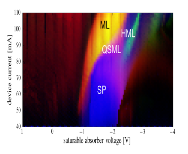
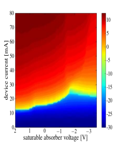
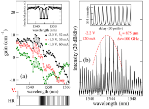
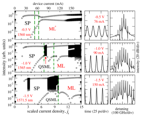
For the plain FP device the measured threshold current with a single current density over the whole device length [single section FP] was 12.5 mA. A measured phase-space map of the dynamical states of the device as the device current and reverse bias voltage applied to the short section are varied is shown in the upper panel of Fig. 1. One can see that a large region of self-pulsations [SP] is found near to threshold, and that these tend to evolve into mode-locked [ML] operation through a region of Q-switched mode-locking [QSML]. The current range where QSML is found becomes wider as the reverse bias is increased, and harmonic mode-locking [HML] is also found in a small region for large negative values of the absorber bias. A map of the power output of the device is also shown in the upper panel of Fig. 1. This shows an increasing threshold current until approximately -1.5 V, where an anomalous decrease is found for increasing negative bias.
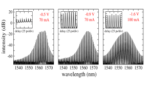
In the lower panel of Fig. 1 we have included optical spectra and the corresponding intensity autocorrelation measurements at three points in the phase space of Fig. 1. We observe incomplete mode-locking at small values of the reverse bias around -0.5 V. Well developed mode-locking of the FP device is found near a device current of 70 mA, and a reverse bias voltage of -1.0 V. In this region the device generates pulses of approximately 1.7 ps duration at a repetition rate of 80 GHz. These pulses, which are not transform limited, become shorter as the reverse bias is increased, reaching a minimum duration of approximately 1.5 ps near -1.5 V. Note that the shift of the peak emission wavelength with increasing reverse bias is initially towards longer wavelengths and that this trend is reversed for larger reverse bias voltages. This reversal also occurs in the region of reverse bias voltage values where the threshold variation with increasing bias becomes anomalous.
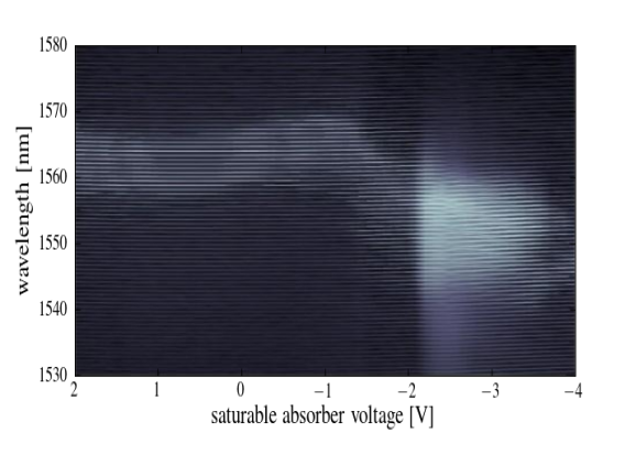
Fig. 2 illustrates the dramatic shifts in the peak emission wavelength that occur in the region of anomalous threshold variation. Here we have shown the optical spectrum of the device as a function of saturable absorber voltage at a fixed device current in the long section of 100 mA. At reverse bias voltages up to approximately -1.5 V, one can see that the peak emission wavelength is relatively constant, with a small drift towards long wavelength. Beyond this region, with increasing reverse bias, we observe a much more rapid shift of the peak emission towards shorter wavelengths.
Experimental data from the second device of length 875 m are presented in Fig. 3 bitauld_10 . In this example the filter was designed to select a comb of six primary modes with 100 GHz spacing at a wavelength of 1545 nm. Net gain measurements near threshold made using the Hakki-Paoli technique are shown in Fig. 3 (a). These data show that the net gain is an increasing function of reverse bias near the location of the spectral filter for reverse bias voltages larger than -1.0 V. Note also that Fig. 3 (a) provides us with a measure of the filter selectivity that can be achieved with etched features in devices such as these. In the device shown, the selectivity is somewhat non-uniform but it reaches a maximum of approximately 2 . We found that the device of Fig. 3 mode-locked near a drive current of 120 mA and reverse bias voltage of -2.2 V to obtain a transform limited 100 GHz pulse train with 2 ps pulse duration [Fig. 3 (b)]. The timing jitter of the pulse train and the phase noise of the individual comb lines also showed significant improvement as compared to an equivalent plain FP laser bitauld_11a , which we attribute to the beneficial effects of thinning of the optical spectrum. The optical spectrum also shows strong suppression of cavity modes between the primary comb lines, which could otherwise be a source of so-called supermode noise quinlan_09 ; srinivasan_14 . However, although we obtained a high quality mode-locking spectrum, the stable ML region was far too small to allow significant tunability of the comb spectrum.
The measurements of Fig. 2 and Fig. 3 (a) suggest that the limited mode-locking range of these devices was due to the complex dispersion of the net modal gain at the location of the spectral filter. In order to address this issue, we have developed a general method for determining the optimal wavelength location for a spectral filter that can lead to a large ML region and associated tunability in the parameter region where the variation of the peak wavelength of the net gain with drive parameters is less pronounced. We have noted that a spectral filter will constrain the active modes of a device so that the carrier wave frequency in the mode-locked state cannot adjust as in the FP. Although a quantitative optimization method would explicitly account for the action of the spectral filter, we will illustrate the application of the method by applying it to a notional device with the same material composition as the two-section FP laser of Fig. 1. However, the method is general, and it could be adapted to models of the two-section device that account for the filter explicitly. We also argue that our results here can be regarded a qualitatively accurate, as we expect model-locking of a narrow-band comb defined by an intracavity spectral filter will not be more difficult than a plain FP laser, provided that the additional modal dispersion due to the filter is limited.
III Model parameter extraction based on an analytical model of the semiconductor modal gain and absorption
In this section we describe the analytic model of the modal gain and absorption that we use to fit measured data. Before we proceed, it is instructive to first introduce the well-known rate equation description of a laser with a saturable absorber [LSA model]. By considering these equations, which are also referred to as the Yamada model yamada_93 , we can introduce the various model parameters that we must obtain in their physical context, and we may also motivate the scaling of the dynamical variables that we will employ in our simulations.
Although the LSA model cannot describe mode-locked states of the device, it is the simplest model that can describe phenomena such as self-pulsations and the appearance of a bistable region at threshold in devices with saturable absorbers dubbeldam_99 . These equations make a total field approximation to describe the intensity of the FP laser, and the saturable absorber section of the laser is described as an unpumped region, with an unsaturated loss determined by the applied voltage. In physical units the LSA model reads
| (1) | |||
Here is the average photon density, is the modal gain and is the modal absorption. and are the carrier densities in the gain and absorber sections, respectively. The total field losses are , where are the mirror losses, and are the internal losses of the device. The current density in the gain section is , while the carrier lifetimes in the gain and absorber sections are and respectively.
To proceed we must establish the dependence of the gain and absorption in the device as a function of carrier density and frequency. Reference balle_98 provides a convenient model that can be fitted to measured gain and absorption obtained using the Hakki-Paoli method. This work developed an analytical expression for the susceptibility of a quantum-well semiconductor material at low-temperature and has been used extensively to model the gain and saturable absorption in simulations of free-running and mode-locked semiconductor lasers javaloyes_10 ; stolarz_11 . While the model results cannot be regarded as quantitative, they nevertheless provide a qualitative description of the material susceptibility that can be used to obtain physically appropriate parameters for dynamical simulations.
The result for the modal gain is balle_98
where is the wavelength, is the carrier density normalised to the transparency value, is the material gain coefficient, and
Here, is the nominal transition wavelength, describes the bandgap shrinkage with increasing carrier density, and is the linewidth of the optical transition. We use a different carrier density variable in the expressions for the modal gain and absorption in Eqns III as we will choose to normalise the model variables with respect to the differential gain, rather than the transparency value of the carrier density.
We now fit this expression to the modal gain of the active material, , which we determine using the Hakki-Paoli technique. For these measurements a single current density over the full length of the device was maintained. The negative offset at long-wavelength gives an estimate of the internal losses, which are assumed to be wavelength independent and uniformly distributed over the device length. The results of the fit that we obtained for two values of the device current are shown in Fig. 4 (a). The mirror losses of the device are . We find that the internal losses, , as indicated in Fig. 4 (a).
From the resulting fit to the data, we determine the value of the carrier density at threshold for the single section FP laser. Fixing the wavelength at the location of the gain peak at threshold, we determine the differential gain at threshold for the FP laser. We then define the threshold gain and differential gain at the gain peak to be equal to 1 in normalized units. This scale then defines our normalized carrier density variable, . We will also define the scaled current density, , where the threshold current density in the single section FP laser is defined to be equal to 1 in normalised units. The variation of the modal gain at the wavelength of the gain peak at threshold as a function of carrier density is shown in Fig. 4 (b). Here have plotted the data in physical units and in normalized units. The value of the differential gain at threshold is . A table of fitting parameters for the susceptibility function is presented in table 1. The values of and at threshold are 2.38 and 1.26 respectively.
| [nm] | [] | [] | [nm] | [] | |
| 1550.0 | 27.0 | 0.73 | 1554.0 | 16.0 |
To determine the modal absorption in the reverse bias section, , we employ a differential Hakki-Paoli technique. The modal absorption is found from the difference between the modal gain measured with a uniform current density over the whole device length and the modal gain, , measured with the same current density applied to the long section and a given voltage applied to the short section. The relationship is stolarz_11 ; scheibenzuber_11
To fit the derived absorption curve we use the expression
where is the carrier density normalised to the transparency value as before, the material absorption coefficient, , is now a function of voltage, and
Here we have neglected the parameter as the carrier density is taken to be much smaller in the reversed biased section. However, in order to obtain a reasonable fit to the data we have had to introduce a voltage dependent bandgap wavelength . We have also included an additional carrier density and voltage independent contribution to the absorption in the absorber section, . This was necessary because, while the above expression can fit the absorption function accurately near the bandedge, we found that the derived carrier density was close to the transparency value, which led to an unphysically large value for the differential absorption of the material. We therefore included a small offset, , in order to obtain accurate fits of the function with small values of the carrier density appropriate for a reverse biased section. Note also that the transition linewidth in the absorber section was taken to be . This change in the value of the transition linewidth and the voltage dependence of are consistent with the quantum-confined Stark effect stolarz_11 .
Experimental and fitted absorption curves for four values of the reverse bias voltage are shown in Fig. 5 (a). In each case, at short wavelengths, the experimental curves show a region of decreasing absorption with decreasing wavelength. This non-monotonic dependence is consistent with the measurements of Fig. 3 and it is not described by our model absorption function. The result is that fits to these absorption curves are only accurate for wavelengths above a characteristic cutoff that depends on the applied voltage. In all cases however, one can see that the fits are very close to the measured data for wavelengths larger than approximately 1555 nm. From the optical spectra of the lower panel of Fig. 1 and from Fig. 2, we can see that the peak emission wavelength begins to shift towards short wavelengths and approach 1555 nm only for reverse bias voltage values of -1.5 V or larger. These values also define the boundary of the region of rapid variation of the peak emission with voltage, which will result in poor tunability of the ML spectrum. For this reason we will illustrate the application of our optimization method targeting reverse bias voltages between -1.0 V and -1.5 V, and assume that our fits to the absorption are accurate at all wavelengths of interest over this voltage range. A table of fitting parameters for the modal absorption function obtained for voltages ranging from -0.5 to -1.5 V are shown in table 2. Here is the value of the carrier density used to fit the measured [unsaturated] absorption.
| bias | ||||||||
|---|---|---|---|---|---|---|---|---|
| [V] | [nm] | [] | [nm] | [] | ||||
| -0.5 | 1558.0 | 22.75 | 0.33 | 1560.0 | 0.38 | 1.36 | 0.79 | 1.39 |
| -1.0 | 1564.0 | 20.75 | 0.25 | 1565.0 | 0.43 | 1.43 | 0.68 | 1.40 |
| -1.5 | 1572.0 | 18.25 | 0.18 | 1571.5 | 0.49 | 1.60 | 0.54 | 1.41 |
In order to define our model parameters, we must choose a reference wavelength and a carrier density value for each device section where the modal gain and absorption functions are linearized. For the gain variable, we expand around the carrier density value that corresponds to the threshold gain assuming a transparent absorber section: , where . For the absorber section, we linearize the absorption function at the saturation value of the carrier density, and define the carrier density variable so that the unsaturated modal losses, , correspond to zero carrier density in the absorber section. The modal absorption is then given by . We will see that our choice of linearization point for the short section is appropriate given the location of the stable mode-locking region far from threshold, where the absorber is strongly saturated.
Results for a reverse bias voltage of -1.0 V are illustrated in Fig. 5 (b) and (c), where we have plotted the modal gain and absorption as a function of carrier density at the reference wavelength indicated by the vertical line in Fig. 5 (a). We will explain how this wavelength was chosen in the next section. The differential gain at the threshold carrier density assuming a transparent absorber section is or in physical units, and the differential absorption at the saturation value is or (here we have quoted values for the differentials that account for the difference in the device section lengths). The calculated differential gain and differential absorption for voltages ranging from -0.5 to -1.5 V are shown in table 2. Here we have also included the reference wavelength , to be derived in the next section, the unsaturated losses, , and the threshold carrier density as defined above. The differentials are given in dimensionless units defined by the total losses .
IV Delay-differential mode-locked laser model and device optimization method
The results of the previous section have provided us with a qualitatively accurate picture of the variation of the modal gain and absorption in the FP device as functions of carrier density, wavelength and reverse bias voltage. In this section we introduce the delay-differential model of the two-section device, and we describe our method for finding the optimum wavelength location for a spectral filter based on the measured material dispersion. In order to test the accuracy of the delay-differential model, our first objective will be to reproduce a portion of the phase-space structure shown in Fig. 1, concentrating on the region where the variation of the threshold current with reverse bias voltage is normal.
The delay-differential lumped element model that we employ eliminates the spatial dependence of distributed time-domain models in favour of a delay-differential equation for the field variable. As we have discussed, this model accounts for the large gain and loss and the strong saturation of the absorption that are typical of mode-locked semiconductor lasers. It is also suitable for analytic analysis, and it requires minimal computing resources to implement. Although the model is derived assuming a ring-cavity geometry, previous results have shown qualitative agreement with distributed time domain simulations of mode-locking in linear two-section geometries with both quantum well and quantum dot active regions bandelow_06 ; rossetti_11 .
The system of equations is vladimirov_04 ; vladimirov_05 ; raghunathan_13
| (2) | |||
where
and
In the above, is the round-trip time in the cavity, the dynamical variable for the gain is defined as , and the saturable absorption is described by the variable . Here and are respectively the modal gain and absorption, which are now assumed to be spatially varying. is the ratio of the recovery times in the gain and absorber sections, and is the ratio of the material differential gain and absorption. are the linewidth enhancement factors in the gain and absorber sections of the device, and is the detuning of the gain peak from the nearest cavity mode. With the linearized gain and absorption variables defined as in the previous section, the scaled pump current is and the parameter describing the unsaturated absorption is . The parameter determines the bandwidth of the gain medium, which is included in these equations through the action of a linear Lorentzian filter vladimirov_05 .
We have seen that the peak emission wavelength of the FP laser will in general evolve continuously as the drive parameters are varied. On the other hand, for each bias voltage value, each wavelength defines a unique set of model parameters through the modal gain and absorption functions. In order to reproduce the structure of the phase-space of Fig. 1, our approach therefore is to associate a unique wavelength with each point in the phase-space of drive parameters. To do this, we calculate the variation of the net gain along branches of steady-state solutions of Eqns IV. The voltage value and material parameters at each wavelength define a unique branch of steady-state solutions in the current density variable. To compare the model and experiment, we choose the branch whose wavelength coincides with the peak of the net gain at the current density point of interest. This method provides a consistent means to compare the measured phase-space data and the simulation results over the entire parameter space, provided the variation of the net gain is well described by our fitted modal gain and absorption functions. To avoid unnecessary details, we will take -1.5 V as defining a boundary beyond which fitting errors can lead to disagreement between the calculated and measured location of the peak emission wavelength. In practice, one should locate this boundary precisely as a function of device current and define the target ML region for voltages inside this boundary. Note that we should also in principle linearize our modal absorption function at the carrier density value where the net gain peak and the wavelength of the steady-state solution branch in question coincide. However, finding the correct steady-state branch in this case requires a much larger numerical effort, as the dispersion of the net gain at any particular wavelength will vary as the linearized absorption function is changed. Instead, we linearized the modal absorption around the transparency point, which is only approached asymptotically. However, we will see that the absorption is already well saturated inside the large stable mode-locking region of Fig. 1.
To find the correct steady-state solution branches we must first calculate the steady-state solutions of the model. Assuming slowly varying fields with respect to , we neglect the time derivative term in Eqn IV and multiply the resulting equation by its complex conjugate to obtain , where is the optical power. The assumption of slowly varying fields implies that so that we obtain an ordinary differential equation for the optical power rachinskii_06
| (3) |
This equation, together with the equations for the gain and absorption variables in Eqn IV, can be regarded as defining an improved LSA model that is accurate for large gain and loss. In order to find the steady-state solution branches we must specify the values of the carrier recovery times in the gain and absorbing sections of the device. We can estimate the carrier recovery time in the gain section from a measurement of the relaxation oscillation frequency of the single section FP device. If we make the approximation that for the plain FP laser, this quantity is expressed in physical units as
| (4) |
where is the photon lifetime in the cavity and is the group velocity. The relaxation oscillation frequency can in turn be determined from the intensity noise power spectrum bitauld_10 . At a device current of 40 mA , we found that the relaxation oscillation frequency is approximately 4 GHz, from which we determine that or ns. To complete the improved LSA model we must fix the value of the carrier lifetime in the absorber section. This quantity is in general smaller than the recovery time in the gain section, and it is known to have a strong dependence on the applied voltage. To determine for our simulations, we assumed that the recovery time varies as mulet_06 ; karin_94 and took values of ps and = 3.0 V that provided the best agreement with experiment. These values then determine [-0.5, -1.0, -1.5] V = [72, 61, 52] ps.
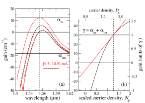
Results showing the variation of the carrier density in both sections of the device along a steady-state solution branch located at a wavelength of 1565 nm for a reverse bias voltage of -1.0 V are shown in the left panel of Fig. 6. In the figure the threshold current density, , for this branch of solutions is indicated. Horizontal lines indicate the threshold carrier density in the gain section, , the threshold carrier density in the gain section, assuming a transparent absorber section, , and the saturated, , and unsaturated, , carrier densities in the absorber section. The wavelength reference was determined by requiring that the peak of the net gain along the steady-state branch coincided with the wavelength reference at a scaled current density [83 mA]. This value was chosen as it lies near the center of the region where we found the highest quality mode-locking in the FP device. The variation of the net gain along the branch of steady-state solutions is shown in right panel of the figure. One can see that the peak of the net gain is located relatively far [5 nm] from the wavelength reference at threshold, with an excess of the net gain of approximately 1.5 . As the current density is increased, the peak of the net gain shifts rapidly towards the wavelength reference, where the net gain is clamped at the value of the total losses . Because the current density region we are targeting here is located far above threshold, we find that the variation of the net gain is minimal over a large range of current density values near the target. This is due to the fact that the absorption is already well saturated in this region, and it justifies our expanding the absorption function around the saturation value of the carrier density. These results also suggest that we can be confident that our choice of model parameters at the wavelength reference will be appropriate for current density values in excess of [59 mA].
We now present numerical bifurcation diagrams calculated using the delay-differential model and compare the results with the experimental measurements from the plain FP laser of Fig. 1. For these simulations the value of , which determines the bandwidth of the Lorentzian filter in Eqns IV, was set as 0.15 ps. This value corresponds to a bandwidth of approximately 80 cavity modes, and it was chosen so that the curvature of the modal gain function at the gain peak was accurately reproduced by the Lorentzian filter. Further parameters were , and . The value of chosen is consistent with our previous work modeling optical injection and feedback experiments in devices with similar material composition osborne_12 .
Numerical bifurcation diagrams calculated for reverse bias values ranging from -0.5 V to -1.5 V are shown in Fig. 7. In each case the value of the wavelength reference is indicated. One can see that the variation of the reference wavelength with bias voltage from 1560 nm at -0.5 V [] to 1565 nm at -1.0 V [] is in broad agreement with the measured variation of the peak emission wavelength visible in the optical spectra shown in Fig. 1. The further red-shift in the reference wavelength to 1571.5 nm that we find for a bias voltage of -1.5 V [] is not in agreement with the measured data for -1.6 V, as this voltage is inside the region where the anomalous dispersion of the material absorption comes into play. However, we will see that the dynamical states of the laser are qualitatively reproduced in this voltage region. If we first compare the simulated device dynamics with measured data at -0.5 V, we find SPs at threshold, followed by a transition to a dynamical state where the intensity is weakly modulated at a frequency close to the round trip time in the cavity. Although SPs at threshold were not resolved in our measurements at this voltage, for larger currents we recall that the corresponding measured behavior was incomplete mode-locking, where a large number of FP modes were above threshold but the intensity modulation at the round trip frequency was also weak. For comparison, we have included a simulated intensity time trace and corresponding optical spectrum at a scaled current density of [76 mA]. One can see that the optical spectrum is almost single mode for these parameters. We have therefore referred to these states as “starred” mode-locked states of the laser, [], as the intensity modulation at the round-trip frequency is very weak in this region. The tentative correspondence between these simulations and our measurements is an indication that the delay-differential model with calibrated parameters can capture subtle physical variations that were found across the ML region in our experiment.
At a reverse bias of -1.0 V, we see that the SP region at threshold increases in size, and we find a narrow region of QSML before entering a region of well developed mode-locking near a device current of 90 mA. This narrow region of QSML is also evident in our experimental measurements for larger reverse bias values. The ML region extends as far as 140 mA, where mode-locking becomes unstable. When compared to our experimental measurements, we can see that the ML region here opens at a larger value of the device current, and that it extends over a larger current range in the simulation. However, one should note that the incomplete ML region near -0.5 V was recorded as a CW region in our measurements, which indicates that there may be a larger region of incomplete ML surrounding the labeled ML region in Fig. 1. If we examine the simulations for -1.5 V in the lower left panel of Fig. 7, one can see that the general trends that were observed in our measurements are well reproduced by the simulations. These include the increasing size of the QSML region, and the rapid expansion of the ML region with increasing reverse bias. One can see also that the pulse duration becomes progressively shorter as the reverse bias is increased. Although the numerical pulse duration at -1.0 V [2.7 ps] is considerably longer than the experimental value, the pulse duration is 1.6 ps at -1.5 V, which is in broad agreement with measured data.
Dashed vertical lines in the bifurcation diagrams of Fig. 7 indicate regions of stable mode-locking calculated using the generalized New stability criterion [GNSC] for the DDE model formulated in Ref. vladimirov_05 . The New stability criterion for mode-locked states requires that the net gain must be negative at the beginning and end of the slow-stage of the dynamics between pulses when the intensity is small new_74 . Although the agreement with the GNSC is poor for smaller reverse bias voltages, at larger reverse bias, where the pulses are well developed, we find this criterion gives a very good estimate for both stability boundaries [the upper ML stability boundary at -1.5 V near is not shown in this figure]. The utility of these semi-analytic results for the ML stability boundaries obtained from Eqns IV highlight an attractive feature of the DDE model, but they also demonstrate that the DDE model has a much richer dynamics and a much larger stable ML region than the GNSC would in general suggest.
The results presented in Fig. 7 demonstrate that the delay-differential model with experimentally calibrated parameters can provide reasonably good qualitative agreement with experimental data. Overall, the model seems to overestimate the drive current required to reach the ML region at a given voltage, and it also overestimates the size of the various regions of dynamics in both the voltage and device current variables. It is clear however that the region of simulated high quality mode-locking evolves from a region of incomplete mode-locking as the reverse bias voltage is increased, which means that we can judge if a simulated ML region is likely to vanish for a small change in the model parameters.
With these qualifications in mind, we now consider the problem of finding the optimal wavelength location for a spectral filter in order to maximize the stable mode-locking region and tunability of the device. If we imagine a relatively narrow-band filter, and a quasi-static picture of the dynamics, then the current and voltage range over which we can expect stable mode-locking at the desired wavelength will be determined by the variation of the net gain along the corresponding steady-state branches at the wavelength location of the spectral filter. To avoid transfer of the optical power to adjacent cavity modes, we require that the excess of the net gain along a steady-state branch at the filter location cannot exceed the filter selectivity at detuned wavelengths. This condition must be then be satisfied over a continuous region in the current and voltage parameters, accounting for the fact that each voltage determines a different steady-state branch at the wavelength of the spectral filter.
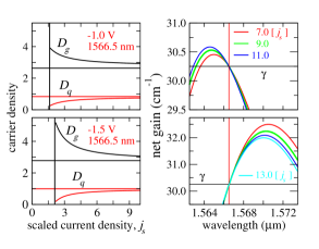
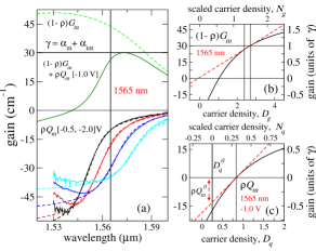
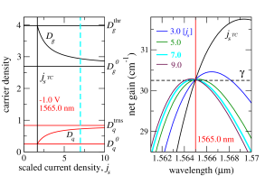
An experimentally calibrated example illustrating the application of this method is shown in Figs 8 and 9, where we have found that a filter located at 1566.5 nm will lead to a large and continuous region of high quality mode-locking near 140 mA for voltages between -1.0 and -1.5 V. Left panels in Fig. 8 show the carrier density along the steady-state solution branches for the two voltages, while the right panels show the variation of the net gain along these branches for between 7 [83 mA] and 13 [154 mA]. Notice how the wavelength reference here is located closer to the peak of the net gain at -1.0 V, which leads to a larger excess of the net gain along the branch at -1.5 V. This was necessary in order to ensure overlapping ML regions in the phase-space as shown in the left panels of Fig. 9. Time traces in the right panels of Fig. 9 indicate well developed pulses over the ML region. Results in Fig. 8 indicate that a spectral filter will require a minimum selectivity of ca. 3 to ensure stable emission at the desired wavelength over this parameter region. Although this value of the filter selectivity exceeds the measured value from the FP device of Fig. 3, we note that this device was based on a low-density grating structure that was defined by etched features in the laser ridge waveguide. Numerical simulations of distributed feedback structures that define comb laser spectra indicate that more advanced grating designs can readily achieve this level of selectivity bitauld_11b ; obrien_14 .
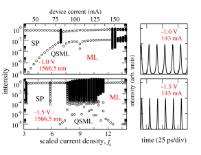
The results of Fig. 9 indicate that a grating spectral filter centered at a wavelength of 1566.5 nm will allow for tuning of the ML state of the device over a wide range in the drive current and voltage parameters. Although the overall device length and absorber section length of the device of Fig. 3 were not identical to the FP laser we considered in order to illustrate the application of the method, the material composition was identical. It is notable therefore that the result for the optimal location of the grating filter is some 20 nm from the designed wavelength location of the device of Fig. 3. We note also that the optimized wavelength location is more than 12 nm from the position of the gain peak at threshold in the FP device.
Because the agreement between the simulated and measured phase-space data for the FP device was only qualitative, our results for the optimized wavelength location and the predicted dynamics are approximate. In particular, we did not account explicitly for any additional dispersion or change in modal thresholds that a grating filter might introduce in the cavity. Numerical results have shown that the grating induced dispersion can become much larger than the underlying material dispersion in devices with strongly scattering filters bitauld_11b . However, it is also possible in general to correct for this in narrow-band examples, which are the focus of our interest here. We also note that the comparison between the simulations and experiment seemed to indicate the presence of some systematic errors, where the onset of mode-locking and the width of the ML region in the current variable was overestimated. It would be interesting to establish if these errors could be eliminated with a more accurate model of the semiconductor susceptibility.
We note also that although the DDE model is a large signal model of the mode-locked laser, our method was based on steady-state solutions of the model and is therefore small signal in nature. We justified this limitation on the grounds that we are interested primarily in mode-locked devices with relatively narrow-band spectra. It would however be interesting to attempt to extend the method in order that it could be applied to devices designed to support wide bandwidth combs, with the potential to generate short pulses. Under these circumstances, the spectrum could be strongly influenced by dynamical effects such as self-phase modulation and the efficiency of the absorber saturation in a mode-locked state bischoff_95 ; javaloyes_10 .
Although we believe that these results demonstrate the utility of the DDE model, our work has also highlighted a number of its limitations. The DDE model is derived assuming a linear Lorentzian spectral filter that corresponds to the gain bandwidth of the semiconductor. However, we obtained unphysical results if we attempted to adjust the filter bandwidth parameter to values that might describe a device such as in Fig. 3. In addition, we found that adjusting the nominal value of the detuning of the gain peak from the nearest cavity mode through the parameter had a significant effect on the simulated phase-space. Given that the gain bandwidth was of order 80 cavity modes, this is also an unphysical dependence of the model. Similarly, we found a strong dependence on the alpha factor values chosen for both sections of the device. Although this dependence is in some respects to be expected, we were unable to interpret our results in a consistent way. We therefore set the alpha parameters to be equal for both sections, and we leave a detailed exploration of the combined roles of the alpha factors and parameter for future work. Overall, it seems that further development of the DDE or a similar model is both necessary and desirable given its obvious strengths. We note that some progress towards generalizing the action of the spectral filter to describe waveguide dispersion in real devices has been already been made heuck_10 .
V Conclusions
In conclusion, we have presented a method for determining the optimal wavelength location for a grating spectral filter in a two-section semiconductor mode-locked laser. The goal of this method was to maximise the region of stable mode-locking in the phase-space of drive parameters of the device. We accounted for material dispersion in the two sections of the laser using a simple analytic model for the semiconductor susceptibility, which provided good agreement with measured data over the parameter region of interest. Our dynamical simulations were based on a delay-differential model of the device, which we found could qualitatively describe the structure of a measured dynamical phase-space when calibrated with experimental parameters. By considering the variation of the net gain along steady-state solutions of the model, we were able to optimize the location of the spectral filter with respect to regions of stable mode-locking in the device. Our results indicate that it will be possible to obtain a large region of stable mode-locking in devices with practical values of the grating selectivity.
The authors acknowledge financial support from Science Foundation Ireland under grant SFI13/IF/I2785.
References
- (1) E. A. Avrutin, J. H. Marsh, and E. L. Portnoi, “Monolithic and multi-GigaHertz mode-locked semiconductor lasers: constructions, experiments, models and applications,” IEE Proc. Optoelectron. 147, 251 (2000).
- (2) R. Kaiser and B. Huttl, “Monolithic 40-GHz mode-locked MQW DBR lasers for high-speed optical communication systems,” IEEE J. Select. Topics Quantum Electron. 13, 125 (2007).
- (3) F. Quinlan, S. Ozharar, S. Gee and P. J. Delfyett, “Harmonically mode-locked semiconductor-based lasers as high repetition rate ultralow noise pulse train and optical frequency comb sources,” J. Opt. A, Pure Appl. Opt. 11, 103001 (2009).
- (4) Y. Ben M’Sallem, Q. T. Le, L. Bramerie, Q.-T. Nguyen, E. Borgne, P. Besnard, A. Shen, F. Lelarge, S. LaRochelle, L. A. Rusch, and J.-C. Simon, “Quantum-dash mode-locked laser as a source for 56-Gb/s DQPSK modulation in WDM multicast applications,” IEEE Photon. Tech. Lett. 23, 453 (2011).
- (5) J. S. Parker, R. S. Guzzon, E. J. Norberg, A. Bhardwaj, P. R. A. Binetti, and L. A. Coldren, “Theory and design of THz intracavity gain-flattened filters for monolithically integrated mode-locked lasers,” IEEE J. Quantum Electron. 48, 114 (2012).
- (6) M. J. R. Heck, P. Munoz, B. W. Tilma, E. A. J. M. Bente, Y. Barbarin, Y. S. Oei, R. Notzel, and M. K. Smit, “Design, fabrication and characterization of an InP-based tunable integrated optical pulse shaper ,” IEEE J. Quantum Electron. 44, 370 (2006).
- (7) S. Srinivasan, A. Arrighi, M. J. R. Heck, J. Hutchinson, E. Norberg, G. Fish, J. E. Bowers, “Harmonically mode-locked hybrid silicon laser with intra-cavity filter to suppress supermode noise,” IEEE Selected Topics Quantum Electron. 20, 1100208 (2014).
- (8) D. V. Strekalov and N. Yu, “Generation of optical combs in a whispering gallery mode resonator from a bichromatic pump,” Phys. Rev. A 79, 041805 (2009).
- (9) S. B. Papp, P. Del’Haye, S. A. Diddams, “Parametric seeding of a microresonator optical frequency comb,” Optics Express 22, 1394 (2014).
- (10) M. Peccianti, A. Pasquazi, Y. Park, B. Little, S. T. Chu, D. J. Moss, and R. Morandotti, “Demonstration of a stable ultrafast laser based on a nonlinear microcavity,” Nature Comms. 3, 765 (2012).
- (11) A. R. Johnson, Y. Okawachi, M. R. E. Lamont, J. S. Levy, M. Lipson, A. L. Gaeta, “Microresonator-based comb generation without an external laser source,” Optics Express 21, 17615 (2014).
- (12) S. O’Brien, S. Osborne, D. Bitauld, N. Brandonisio, A. Amann, R. Phelan, B. Kelly, and J. O’Gorman, “Optical synthesis of terahertz and millimeter-wave frequencies with discrete mode diode lasers,” IEEE Trans. Microwave Theory Tech. 58, 3083 (2010).
- (13) D. Bitauld, S. Osborne and S. O’Brien, “Passive harmonic mode locking by mode selection in Fabry-Perot diode lasers with patterned effective index,” Opt. Lett. 35, 2206 (2010).
- (14) S. O’Brien, “Comb transmission filters defined by phase-shifted superstructure Bragg gratings,” Opt. Lett. 39, 1085 (2014).
- (15) P. M. Stolarz, J. Javaloyes, G. Mezosi, L. Hou, C. N. Ironside, M. Sorel, A. C. Bryce, S. Balle, “Spectral dynamical behavior in passively mode-locked semiconductor lasers,” IEEE Photonics Journ. 3, 1067 (2011).
- (16) D. Bitauld, S. Osborne and S. O’Brien, “Timing characterization of 100 GHz passively mode-locked discrete mode laser diodes,” Opt. Express 19, 13989 (2011).
- (17) J. L. A. Dubbeldam and B. Krauskopf, “Self-pulsations of lasers with a saturable absorber: dynamics and bifurcations,” Opt. Comm. 159, 325 (1999).
- (18) F. O’Callaghan, S. Osborne, and S. O’Brien, “Dispersion-induced dynamics of coupled modes in a semiconductor laser with saturable absorption”, Phys. Rev. A 89, 033848, (2014).
- (19) K. Y. Lau, “Narrow-band modulation of semiconductor lasers at millimeter wave frequencies ( 100 GHz) by mode-locking,” IEEE J. Quantum Electron. 26, 250 (1990).
- (20) E. A. Avrutin, J. M. Arnold and J. H. Marsh, “Dynamic modal analysis of monolithic mode-locked semiconductor lasers,” IEEE J. Selected Topics Quantum Electron., 9, 844 (2003).
- (21) E. A. Avrutin and E. U. Rafailov, “Advances in mode-locked semiconductor lasers.” in Advances in Semiconductor Lasers, vol 86, J. Coleman, A. Bryce and C. Jagadish, Eds. Amsterdam, Holland: Elsevier, 2012, pp. 93-147.
- (22) A. G. Vladimirov, and D. Turaev “Model for passive mode-locking in semiconductor lasers,” Phys. Rev. A 72, 033808 (2005).
- (23) D. Rachinskii, A. Vladimirov, U. Bandelow, B. Huttl, and R. Kaiser, “Q-switching instability in a mode-locked semiconductor laser,” J. Opt. Soc. Am. B 23, 663 (2006).
- (24) S. Bischoff, M. P. Sorensen, J. Mork, S. D. Brorson, T. Franck, J. M. Nielsen and A. Moller-Larsen, “Pulse-shaping mechanism in colliding-pulse mode-locked laser diodes,” Appl. Phys. Lett. 67, 3877 (1996).
- (25) J. Mulet and J. Mork, “Analysis of timing jitter in external-cavity mode-locked semiconductor lasers,” IEEE J. Quantum Electron. 42, 249 (2006).
- (26) J. Javaloyes and S. Balle, “Mode-locking in semiconductor Fabry-Perot Lasers,” IEEE J. Quantum Electron. 46, 1023 (2010).
- (27) A. G. Vladimirov, D. Turaev, and G. Kozyreff, “Delay differential equations for mode-locked semiconductor lasers,” Opt. Lett. 29, 1221 (2004).
- (28) M.Yamada, “A theoretical analysis of self-sustained pulsation phenomena in narrow-stripe semiconductor lasers,” IEEE J. Quantum Electron. 29, 1330 (1993).
- (29) S. Balle “Simple analytical approximations for the gain and refractive index spectra in quantum-well lasers,” Phys. Rev. A 57, 1304 (1998).
- (30) W. Scheibenzuber, U. Schwarz, L. Sulmoni, J.-F. Carlin, A. Castiglia, and N. Grandjean, “Measurement of the tuneable absorption in GaN-based multi-section laser diodes,” Phys. Stat. Solidi, 8, 2345 (2011).
- (31) U. Bandelow, M. Radziunas, A. Vladimirov, B. Huttl and R. Kaiser, “40 GHz mode-locked semiconductor lasers: theory, simulations and experiment,” Optical and Quantum Electronics, 38, 495 (2006).
- (32) M. Rossetti, P. Bardella, and I. Montrosset, “Modeling passive mode-locking in quantum dot lasers: a comparison between a finite-difference traveling-wave model and a delayed differential equation approach,” IEEE J. Quantum. Electron., 47, 569 (2011).
- (33) R. Raghunathan, M. T. Crowley, F. Grillot, Y. Li, J. K. Mee, V. Kovanis, and L. F. Lester, “Pulse characterization of passively mode-locked quantum-dot lasers using a delay differential equation model seeded with measured parameters,” IEEE Select. Top. Quantum Electron. 19, 1100311 (2009).
- (34) J. R. Karin, R. J. Helkey, D. J. Derickson, R. Nagarajan, D. S. Allin, J. E. Bowers, and R. L. Thornton, “Ultrafast dynamics in field-enhanced saturable absorbers,” Appl. Phys. Lett. 64, 677 (1994).
- (35) S. Osborne, P. Heinricht, N. Brandonisio, A. Amann, and S. O’Brien, “Wavelength switching dynamics of two-colour semiconductor lasers with optical injection and feedback,” Semiconductor Sci. Technol. 27, 094001 (2012).
- (36) G. C. H. New, “Pulse evolution in mode-locked quasi-continuous lasers,” IEEE J. Quantum Electron. 10, 115 (1974).
- (37) D. Bitauld, S. Osborne and S. O’Brien, “Design of waveguide-integrated semiconductor laser sources for optical frequency comb generation,” Opt. Lett. 36, 2985 (2011).
- (38) M. Heuck, S. Blaaberg, and J. Mork, “Theory of passively mode-locked photonic crystal semiconductor lasers,” Optics Express 18, 18003 (2010).