Photovoltaic performance of n-type SnS active layer in ITO/PEDOT:PSS/SnS/Al structure
Abstract
The present paper discusses the influence of Tin Sulphide’s grain size on the performance of ITO/PEDOT:PSS/SnS/Al structured solar cells fabricated by thermal evaporation. The grain sizes were maintained in the range of 11-18 nm by controlling the thickness of SnS films. While the open circuit voltage () was found to be a constant for this structure, parameters such as short circuit current density (), series resistance (), parallel resistance (), ideality factor and the overall efficiency were found to be dependent on the SnS grain size and incident light intensity. The experimental work directly reconfirms the theoretical results and ideas raised in literature by early researchers.
keywords:
Thin Films; Chalcogenides; Solar Cells1 Introduction
With the depleting reserves of fossil fuels and its adverse effects on the environment, efforts are being made to search for environment friendly and renewable sources of energy. Solar energy seems to be the most promising candidate. These days research is focussed on the development and fabrication of high efficiency and low cost photo-voltaic devices. Photo-voltaics are usually p-n devices with active region having enough absorption coefficient to absorb the incident light yet thin enough for charge carriers to reach their respective electrodes without recombination. Thin film technology suits the demands and active layer of few micrometer thickness are fabricated by various fabrication techniques.
Inorganic thin film solar cells have always been considered as one of the main cost-effective options for the future photovoltaic devices. In recent years chalcogenide materials such as PbS [1], PbSe [2], CdS [3], CdTe [4], SnS [5] and [6] have attracted attention. The best efficiency that has been reported was using CdS/CdTe at [7]. However, due to the toxic nature of Cadmium and its compounds, Cadmium compounds rule themselves out as a candidate [8]. Tin Sulphide (SnS) promises to be the most suitable candidate for solar cells [5, 9] due to its optimum optical properties which are tunable by varying the grain size and/ or lattice parameters [10, 11, 12]. SnS films also have high absorption coefficients [13, 14] and optical band-gap in the range of 1.1-2.1 eV [15, 16]. On top of all this, SnS is non toxic [17] and easily available [18]. However, structures with only SnS do not show photo-voltaic behavior [19].
Table 1: Comparison of properties of SnS based solar cells from the literature listed in order of increasing efficiency.
| S.No. | Structure | Grain Size (nm) | (mA/) | (V) | Ref | |
|---|---|---|---|---|---|---|
| 1. | ITO/PEDOT:PSS/Polymer:SnS/Al | 10 | 0.055 | 0.84 | 0.0205 | [17] |
| 2. | ITO/CdS/SnS/Al | 20-40 | - | 0.2 | 0.09 | [20] |
| 3. | ITO/CdS/SnS/Al | - | 1.23 | 0.37 | 0.2 | [21] |
| 4. | FTO//SnS Quantum dots/Pt | 5.06 | 2.3 | 0.504 | 0.2 | [22] |
| 5. | ITO/PbS/SnS/Al | 9.6 | 1.2 | 0.44 | 0.27 | [19] |
| 6. | ITO/CdS/SnS/Ag | 300 | 7 | 0.12 | 0.29 | [14] |
| 7. | /SnS/CdS:In/In | 350 | 9.6 | 0.26 | 1.3 | [8] |
Research work have hence shifted focus towards hetero-junction structures of SnS, for example CdS/SnS [20, 21], SnS/PbS [19], SnS quantum dots on [22] and SnS nanoparticles embedded in polymer [17] hetero-junction structures. Table 1 summarizes the photo-voltaic performance along with grain size of the SnS active layer. Interestingly, Noguchi et al [14] obtained a more efficient photo-voltaic () with the same structure used by Ghosh et al [20] and David et al [21]. While David et al [21] obtained their active SnS layer by chemical deposition, Noguchi et al[14] used thermal evaporation to obtain their active layer. Interesting, for the same structure, Reddy et al. [8] improved upon Noguchi et al [14] using SnS films of larger grain size obtained by spray pyrolysis (). These studies show that there is a co-relation between the active layer’s grain size and structure’s efficiency.
It is clear from the above discussion and results listed in Table 1 that the granularity of the film affects the performance of photo-voltaic devices. Hence, it would also be of fundamental interest to enquire how the grain size influences solar cell parameters such as open circuit voltage (), short circuit current density () etc. Therefore, we decided to revisit a simple photo-voltaic structure involving a tin sulphide active layer. The effect of the active layer’s grain size and illumination intensity on the device parameters (and hence its performance) have been investigated.
2 Experimental Details
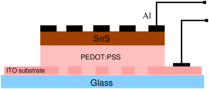
For the present study, Indium Tin Oxide (ITO) substrates were used. ITO has been a popular choice as a substrate in solar cells because of its high conductivity and transparency at room temperature [23]. This feature allows the substrate to double as an electrode of the device on proper etching. We have used an ITO substrate of low resistivity (). On the etched ITO substrates, a thin buffer layer (200 nm) of solar grade PEDOT:PSS (1.3 weight %) was spin coated, followed by which the substrates were dried in a vacuum furnace at 373 K. This gives an uniform, conducting and transparent layer that stabilizes the etched surface of ITO substrate. This layer also favors the hole injection and collection at the electrode [24]. Our attempts to fabricate simple ITO/SnS/Al structures (i.e. without PEDOT:PSS) failed to give typical IV characteristics of photo-voltaic devices. The failure of the simple ITO/SnS/Al structures has been reported earlier too [19]. The active layer (SnS thin film) was deposited on the ITO/PEDOT:PSS substrate which was maintained at room temperature. During the deposition, glass substrates were placed alongside ITO/PEDOT:PSS substrates. Films on glass substrates were used only for hotprobe tests to determine the nature of charge carriers present in them. The films grown on ITO/PEDOT:PSS were divided into two parts, one for solar cell fabrication and second for characterization. The photovoltaic structure was completed by depositing Aluminium electrodes, again by thermal evaporation using standard mask giving electrodes of area . Thus, we zeroed down to an ITO/PEDOT:PSS/SnS/Al structure similar to that used by Wang et al [17]. Fig 1 shows the cross-sectional view of the final structure. The current-voltage (J-V) measurements were done with a computer monitored Keithley 2400 source meter unit. A solar simulator of variable illumination intensity served as the light source.
For characterization the thicknesses of the active layers were measured using Veeco’s Dektak Surface Profiler (150). The nano/poly-crystallinity of the active layers was determined by X-ray diffraction (XRD) (Bruker D8 X-ray Diffractometer) of radiation () in the configuration. The surface morphology of the samples was determined using a Field Emission-Scanning Electron Microscope (FE-SEM FEI-Quanta 200F) at an accelerating voltage of 10 kV.
3 Characterization of SnS films

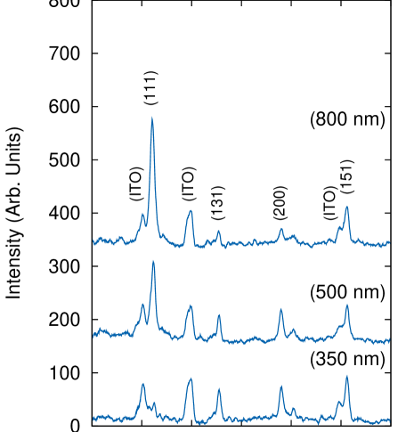
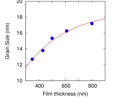
The structure of the SnS films on ITO/PEDOT:PSS substrates were studied using X-ray Diffraction. Fig 2 shows the diffraction profiles of the SnS films of various thicknesses. Four prominent diffraction peaks at , , and were identified from the (111), (131), (200) and (151) crystal planes respectively of tin sulphide with orthorhombic unit cell structure of lattice parameters a=4.148, b=11.36 and c=4.177 (ASTM No.83-1758). The remaining peaks of fig 2 (marked) are those of the ITO layer [25]. The SnS films on ITO substrates were oriented with the the (111) planes perpendicular to the substrate [25, 26]. The average grain size of the films were also calculated using the well known Scherrer formula [27]. The grain size was found to increase with film thickness (fig 2). The grain size tends to saturate for large thicknesses (). However, the grain size variation with thickness is linear for the range 350-600 nm.
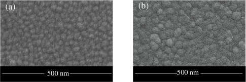
Fig 3 shows the Scanning Electron Microscope (SEM) images of the SnS films (thickness 500 and 800 nm). The images show that the grains are spherical in nature. In our recent works [10, 11, 12], we have grown SnS films on glass substrates which resulted in films oriented with (040) planes parallel to the substrate or in other words the larger ‘b’ edge of the unit cell were arranged along the substrate. This resulted in elongated SnS grains on glass substrates. However, the (111) orientation on ITO substrates seems to prefer spherical grain formation [25, 26, 28]. Hotprobe measurements reveal that the SnS films used in this study are n-type without exception. Literature reports SnS films can either be of p-type or n-type, depending on fabrication conditions [28]. Clearly, we have been able to maintain our sample fabrication conditions throughout our study. Also, considering that our SnS films were n-type, PEDOT:PSS conducting polymer serves as the p-type layer, thus forming an inorganic-organic hetergenous solar cell structure [29]. Fig 4 shows the energy level diagram of our structure. The value of work functions were take from literature [29, 30]. The highest occupied molecular orbital (HOMO) level of the PEDOT:PSS lies below the valence band of SnS, hence the photo-generated holes at the junction easily drift towards the PEDOT:PSS layer while it acts as a barrier for electrons generated. The electrons move towards the Al electrode.
Summarizing our above results, tin sulphide films grown by thermal evaporation give oriented films of n-type on ITO substrates, whose spherical shaped grains increase in size with increasing film thickness. We believe the above results would be of essence in establishing a relation between performance and fabrication conditions.
4 Solar Cells
For characterization of our solar cells we have made Current-Voltage (I-V) measurements for all our samples. It is an industry standard to make measurements of solar-cells at room temperature with illumination intensity of 100 mW/ of Air Mass (AM) 1.5 spectrum for performance comparison. While we have made measurements at various illumination intensities (summarized in Table 2), in the following passages we detail our device’s performance under illumination.
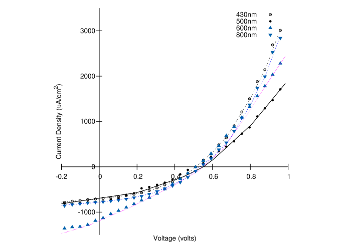
Fig 5 gives the J-V characteristics of our solar cells. Various models like single-diode, two-diode models [31] etc. are used to evaluate the characterizing parameters of solar cells from which their efficiencies are calculated. While the single-diode model emphasizes on the junction formed due to the ‘p’ and ‘n’ layer, the two-diode model takes into account the recombinations occuring across the grain boundaries of a polycrystalline active layer. If the recombination across the grain boundaries are insignificant compared to the contributions from the pn junction or if its contribution is constant (i.e. is not a function of applied voltage/current) then the single diode model can be applied on polycrystalline active layers too [31]. Decision is based on the nature of J-V curve in the first quadrant. For linear variation [31, 32] a single-diode best models the behavior of the solar cells. Fig 6 shows the equivalent single-diode model of a solar cell. All the research groups listed in Table 1 agree that nano/polycrystalline SnS has linear J-V characteristics in the first quadrant and hence have used the single diode model to characterize their solar cells. However, it is interesting to note that while the recombination across grain boundary might be insignificant, grain size does play a significant role as can be seen from improved efficiency with grain size (Table 1).
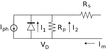
As can be understood from fig 6, we need to determine the series resistance () and parallel resistance () for characterizing the solar cell completely. This is important since these internal resistances decide parameters like the open circuit voltage (), the short circuit current density (), the ideality factor (n), the Fill Factor (FF) and ultimately the peak power (). The internal resistances were estimated from the slopes of the J-V curve as per the single diode model [17]
| (1) | |||||
| (2) |
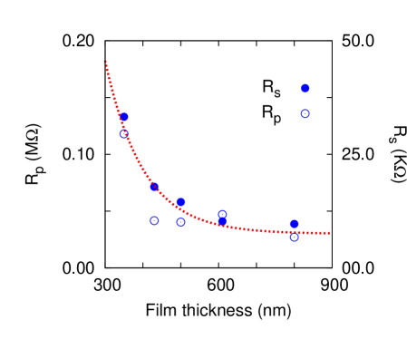
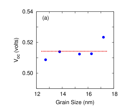
is the open circuit voltage i.e. the voltage at which no current flows through the external circuit. This is directly obtained from fig 5 as the point where experimental curve cuts the ‘X’-axis. The short circuit current (), is the current that flows in the external circuit when the electrodes are short circuited (again, obtained from fig 5 as the point where experimental curve cuts the ‘Y’-axis). We have evaluated and as a function of film thickness. Both the resistances are found to decrease with increasing film thickness (fig 7). Interestingly, the trends are identical for both the resistances with , (). The variation in these resistances with grain size also shows a similar trend (not shown). The resistance appears from the Al electrode to an imaginary point within the bulk of the SnS active layer. Thinner films have smaller grain size and in-turn larger inter-grain boundary voids. This can be seen in the micrographs of fig 3. These inter-grain voids would contribute large resistances which decreases with increasing film thickness [33]. Fig 8a shows the variation in the open circuit voltage and short circuit current density with the grain size. The open circuit voltage was found to be constant () within experimental error. The value of we report is higher as compared to similar structures reported in literature [8, 14]. The open circuit voltage is essentially the voltage across and is reported to be constant for large values of [34]. Considering Renu et al [34] have indicated as large, with our parallel resistances laying in the range of , we expect to be constant.
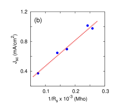
Also we find that the current density (), increases with increasing grain size (fig 8b). Considering that we are talking of the short circuited current and , this current would essentially be flowing through . As explained above, the series resistance is essentially due to the active layer, hence, it would be the prime cause of variation in . Such suggestions, where the short circuit current density is a function of the absorbing layer thickness [21] or grain size [35, 36] have been reported before. Hence, to test the argument that the grain size influences the series resistance which inturn effects , we investigated the variation of with respect to . The prefect linearity confirms that larger grain size results in larger . This is also conveyed by the data of Table 1.
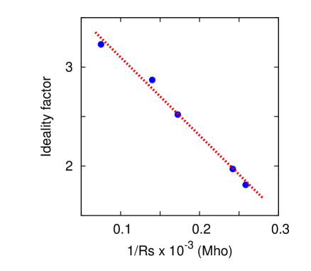
Another important parameter that affects the performance of the solar cell is the diode’s ideality factor (n). For an ideal solar cell the ideality factor is equal to unity [32] implying no recombinations take place as the charge carriers are moving away from the junction to the electrodes. A higher ‘n’ implies recombinations are taking place along the path of the travel. These recombinations maybe taking place at the grain boundaries or within the grains due to defects. With the I-V characteristics near linear in the first quadrant, we have used a single diode model to analyze our device. By not considering the two diode model, we are ruling out the possible contributions from the grain boundaries. The ideality factor for all the cells were evaluated at (V,I)=(0,) (fig 5) using the equation
| (3) |
where is the reverse saturation current obtained from the dark I-V characterisitics. The above equation is derived on the assumption . Fig 9 shows that the ideality factor of the cell decreases and approaches the value for an ideal cell () [32] as the series resistance decreases or grain size increases. Which means that larger the grain size with lower defects results in fewer recombinations in the active layer and hence a smaller ideality factor.
Along with the effect of active layer thickness on the solar cell parameters, we also studied the effect of light intensity on these parameters. Charactering parameters of the cells were evaluated for various incident illumination intensities. Table 2 lists the results for a solar cell with active layer of 500 nm thickness. Both the series resistance () and shunt resistance () decrease with the illuminaiton intensity. This decrease can be attributed to an increase in conductivity of SnS with the increase in the illumination intensity [37, 38]. This also explains the increase in short circuit current with increasing illumination. However, the decrease in contributes to a very small increase in . With the increase in the intensity, the device’s ideality factor also approaches that for an ideal solar cell. This is possibly due to the increased kinetic energy imparted to the charge carriers that lead to a decrease in the recombinations. Though the efficiency of the device does show an enhancement with increasing intensity, the enhancement is not that significant.
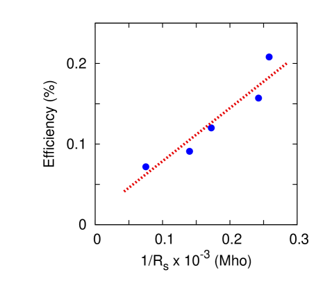
As explained in the introduction, research trends on solar cell technology is concentrated on an effort to improve the efficiency of the solar cell. Efficiency is basically the maximum power generated by the solar cell for the light intensity flux (or power) incident on it. The results we presented here are for an of of Air Mass (AM) 1.5 spectrum. The maximum power, was evaluated for the experimental data of fig 5. The solar cell efficiency was found to vary with grain size. The variation in efficiency with is shown in fig 10. As argued for fig 8(b), this shows the dependency of efficiency on grain size. Clearly, the performance of the solar cell improves with larger grain size. Even from Table 1 it is clear that the efficiency of SnS solar cells increase with grain size, for example, the efficiency varied from [17] to [8] for grain size varing from 10 nm to 350 nm. However, our structure with 10-20 nm grains in the SnS active layer out-preforms the Wang’s [17] similar structured cell with same grain size. Fact that efficiency increases with grain isze argues for solar cells to be made from single crystal wafers. This, however, would push the cost of these devices up. Hence, it would be necessary to study whether plasmonic solar cells of SnS thin films would be of any practical benefit. As an ending note it is necessary to point out that the experimental results of our work directly confirm the intutively indicated ideas of Ghosh et al [20] and those given theoretically by Guliani et al [34].
Table 2: Comparison of ITO/PEDOT:PSS/SnS/Al structure under different illumination intensities.
| Parameter | Intensity () | ||||||
|---|---|---|---|---|---|---|---|
| 2 | 15 | 30 | 100 | ||||
| (mV) | 500 | 505 | 516 | 512 | |||
| () | 3.17 | 26.30 | 55.34 | 182.61 | |||
| () | 116.0 | 87.5 | 61.0 | 2.94 | |||
| () | 2.10 | 0.29 | 0.11 | 0.05 | |||
| % | 0.13 | 0.14 | 0.14 | 0.15 | |||
| Ideality factor (n) | 2.28 | 2.1 | 2.01 | 1.97 |
5 Conclusion
Photovoltaics of ITO/PEDOT:PSS/SnS/Al were fabricated and studied by varying the SnS active layer thickness. The varying thickness was found to alter the grain size of the nano-crystalline thin films. The fitting to the single diode model gave parameters that indicated larger grain sized films gave higher electron-hole generation () and a lower series resistance, . The device’s efficiency was also found to be series resistance dependent.
This series resistance in turn depends on the inter-granular distances or distance between the two grains of the nano-crystalline/ polycrystalline active layer. The incident photons on the solar cells generate charge carriers that rush to their respective electrodes. While inter-grain boundaries are sites of recombination which lead to decrease in the number of charge carriers reaching the electrode (the ‘p’ charge carriers reaching the ITO anode), in our case they offer a large resistive path. So for easy flow of the charge carriers we would require a smaller series resistance or in other words less or no grain boundaries. This would call for a single crystal active layer. This would clearly mean increased cost of production and doing away with simple fabrication technique of thin film coating. Hence, we believe future research would have to focus on methods to tailor materials so as to decrease the series resistances even for nano/poly-crystalline active layers.
Acknowledgment
Authors are thankful to the Department of Science and Technology for funding this work under research project SR/NM/NS-28/2010. We also convey our sincere thanks to Prof. Vinay Gupta, Department of Physics and Astrophysics, University of Delhi for the help rendered.
References
- [1] Piliego C., Protesescu L. , Bisri S.Z. , Kovalenkobc M.V., Loi M.A., 5.2% efficient PbS nanocrystal Schottky solar cell, Energy Environ. Sci. 6 (2013) 3054.
- [2] Schaller R.D., Klimov V.I., High Efficiency Carrier Multiplication in PbSe Nanocrystals: Implications for Solar Energy Conversion, Phys. Rev. Lett. 92 (2004) 186601.
- [3] Wagner S., Shay J.L., Bachmann K.J., Buehler E., p−InP/n−CdS solar cells and photovoltaic detectors, Appl. Phys. Lett. 26 (1975) 229.
- [4] Oladeji I.O, Chow L., Viswanathan V., Zhao Z., Metal/CdTe/CdS/Cd1−xZnxS/TCO/glass: A new CdTe thin film solar cell structure, Sol. Energy Mater. Sol. Cells 61 (2000) 203.
- [5] Ristov M., Sinadinovski G., Mitreski M., Ristova M., Photovoltaic cells based on chemically deposited p-type SnS, Sol. Energy Mater. Sol. Cells 69 (2001) 17.
- [6] Wagner G., Kaden R., Lazenka V., Bente K., Microstructure of grown by hot wall technique., Phy. status solidi, 9 (2011) 2150.
- [7] Mohamed H.A.,Dependence of efficiency of thin-film CdS/CdTe solar cell on optical and recombination losses, J. Appl. Phys. 113 (2013) 093105.
- [8] Reddy K.T.R., Reddy N.K., Miles R.W., Photovoltaic Properties of SnS based solar cells. Sol. Energy Mater. Sol. Cells, 90 (2006) 3041.
- [9] Sinsermsuksakul P., Heo J., Noh W., Hock A.S., Gordon R.g., Atomic layer deposition of Tin Monosulfide Thin Films. Adv. Energy Mater., 1 (2011) 1116
- [10] Jain P., Arun P., Parameters influencing the optical properties of SnS thin films., J. of Semicond., 34 (2013) 093004-1.
- [11] Jain P., Arun P., Influence of Grain Size on the Optical Band-gap of Annealed SnS thin films., Thin Solid Films., 548 (2013) 241.
- [12] Jakhar A., Jamdagni A., Bakshi A., Verma T., Shukla V., Jain P., Sinha N., Arun P., Solid State comm., 168 (2013) 31.
- [13] Thangaraju B., Kaliannan P., Spray pyrolytic deposition and characterization of SnS and SnS2 thin films., J. Phys. D.: Appl. Phys 33 (2000)1054.
- [14] Noguchi H., Setiyadi A., Tanamora H., Nagatomo T., Omoto O., Characterization of vacuum-evaporated tin sulfide film for solar cell materials., Sol. Energy Mater. Sol. Cells, 35 (1994) 325.
- [15] Gao C., Shen H., Sun L., Preparation and properties of zinc blende and orthorhombic SnS films by chemical bath deposition., Appl Surf Sci 257 (2011)6750.
- [16] Sohila S., Rajalakshmi M., Ghosh C., Arora A.K., Muthamizhchelvan C., Optical and Raman scaterring studies on SnS nanoparticles., J. Alloy Compd. 509 (2011) 5843.
- [17] Wang Z., Qu S., Zeng X., Liu J., Zhang C., Tan F., Jin L., Wang Z., The application of SnS nanoparticles to bulk heterojunction solar cells., J. Alloys Comp 482 (2009) 203.
- [18] Yue G.H., Peng D.L., Yan P.X., Wang L.S., Wang W., Luo X.H., Structure and optical properties of SnS thin film prepared by pulse electrodeposition, J. Alloy Compd. 468 (2009)254.
- [19] Stavrinadis A., Smith J.M., Cattley C.A., Cook A.G., Grant P.S., Watt A.A.R., SnS/PbS nanocrystal heterojunction photovoltaics., J. Nanotech. 21 (2010) 1.
- [20] Ghosh B., Das M., Banerjee P., Das S., Fabrication of vacuum-evaporated SnS/CdS heterojunction for PV applications., Sol. energy Mater. Sol. Cells 92 (2008) 1099.
- [21] Avellaneda D., Nair M.T.S., Nair P.K., Photovolatic structures using chemically deposited tin sulfide thin films., Thin solid films 517 (2009) 2500.
- [22] Deepa K.G., Nagaraju J., Growth and photovoltaic performance of SnS quantum dots., Mater. Sci. Engineer. B 177 (2012) 1023.
- [23] Gunes S., Neugebauer H., Sariciftci N.S., Conjugated Polymer-Based Organic Solar Cells., Chem. Rev. 107 (2007) 1324.
- [24] Kim W., Kim N., Kim J.K., Park I., Choi D.H., Chael H., Park J.H., Polymer Bulk Heterojunction Solar Cells with PEDOT:PSS Bilayer Structure as Hole Extraction Layer., Chem. Sus. Chem. 6 (2013) 1070.
- [25] Ghosh B., Das M., Banarjee P., Das S., Fabrication and optical properties of SnS thin films by SILAR method., Appl. Surf. Sci. 254 (2008) 6436.
- [26] Devika M., Reddy N.K., Ramesh K., Sumana H.R., Gunasekhar K.R., Gopal E.S.R., Reddy K.T.R., The effect of substrate surface on the physical properties of SnS films., Semicond. Sci. Technol. 21 (2006) 1495.
- [27] Cullity B.D., Stock S.R., ”Elements of X-ray Diffraction”, 3rd Ed., Prentice-Hall Inc (NJ,2001)
- [28] Sajeesh T.H., Warrier A.R., Kartha C.S, Vijayakumar K.P., Optimization of parameters of chemical spray pyrolysis technique to get n and p-type layers of SnS, Thin Solid Films 518 (2010) 4370.
- [29] Thiyagu S., Hsueh C-C., Liu C-T., Syu H-J., Lin T-C., Lin C-F., Hybrid Organic Inorganic heterojunction solar cells with 12% efficiency by utilising flexible film-silicon with a hierarchical surface, Nanoscale 6 (2014) 3361.
- [30] Devika M., Reddy N.K., Patolsky F., Gunsekhar K.R., Ohmic contacts to SnS films: Selection and estimation of thermal stability, J. Appl. Phys., 104 (2008) 124503.
- [31] Kassis A., Saad M., Analysis of multi-crystalline silicon solar cells at low illumination levels using a modified two-diode model., Sol. Energy Mater. Sol. Cells 94 (2010) 2108.
- [32] Sze S.M. ”Physics of Semiconductor Devices”, 2nd Ed., John Wiley and Sons, Inc. (1981).
- [33] Arun P., Tyagi P., Vedeshwar A.G., Large Grain Size Dependence of Resistance of Polycrystalline films, Physica B 322 (2002) 289.
- [34] Guliania R., Jain A., Kapoor A. Exact Analytical Analysis of Dye-Sensitized Solar Cell: Improved Method and Comparative Study. J. Open Renewable Energy, 2012, 5:49.
- [35] Werner J.H., Dassow R., Rinke T.J., Kohler J.R., Bergmann R.B., From polycrystalline to single crystalline silicon on glass., Thin Solid Films 383 (2001) 95.
- [36] Deceglie M.G., Kelzenberg M.D., Harry A.A Effects of Bulk and Grain boundary recombination on the Efficiency of Columnar-Grained /crystalline Silicon Film Solar Cells. Proceedings of the 35 IEEE Photovoltaic Specialists Conference (preprint)
- [37] Khan F., Singh S.N., Husain M., Effect of illumination intensity on cell parameters of a Silicon solar cell, Sol. Energy Mater. Sol. Cells, 94 (2010) 1473.
- [38] Batzner D.L., Romeo A., Zogg H., Tiwari A.N., CdTe/CdS solar cell performance under low irradiance, presented ( EC PVSEC) Munich (2001).