Clustered impurities and carrier transport in supported graphene
Abstract
We investigate the effects of charged impurity distributions and carrier-carrier interactions on electronic transport in graphene on SiO2 by employing a self-consistent coupled simulation of carrier transport and electrodynamics. We show that impurity clusters of characteristic width 40–50 nm generate electron–hole puddles of experimentally observed sizes. In the conductivity versus carrier density dependence, the residual conductivity and the linear-region slope are determined by the impurity distribution, and the measured slope can be used to estimate the impurity density in experiment. Furthermore, we show that the high-density sublinearity in the conductivity stems from carrier-carrier interactions.
pacs:
72.80.Vp, 81.05.ue, 72.10.-dI Introduction
Graphene, a single sheet of carbon with a honeycomb lattice, is a two-dimensional (2D) material whose high carrier mobility and carrier density tunable by a back gate Castro Neto et al. (2009); Das Sarma et al. (2011); Avouris (2010); Young and Kim (2011); Schwierz (2010) make it attractive for electronic device application Bonaccorso et al. (2010); Kim et al. (2009, 2010); Lin et al. (2010); Sensale-Rodriguez et al. (2012); Otsuji et al. (2012); Schedin et al. (2007); Pumera (2011). Large-area, good-quality graphene is commonly fabricated by chemical vapor deposition (CVD) on metal substrates Yu et al. (2008); Kim et al. (2009); Li et al. (2009), followed by transfer onto insulating substrates using polymers, such as poly-dimethyl siloxane (PDMS) or poly-methyl methacrylate (PMMA). An important concern with these processing methods is the contamination of graphene with organic molecules Meyer et al. (2007), residues of the transfer polymer and metal ions Lin et al. (2012), or charged impurities trapped in the supporting substrate Casiraghi et al. (2007).
Impurities near graphene are believed to be responsible for several observed transport properties. Spatial inhomogeneities in the carrier density, known as electron–hole puddles, are formed due to the presence of charged impurities in the substrate Martin et al. (2008); Zhang et al. (2009); Rossi and Das Sarma (2008). The charged impurities and the resulting electron–hole puddles have been linked to the observed non-universal minimum conductivity (also known as residual conductivity) of graphene close to the Dirac point Adam et al. (2007). However, high-resolution scanning tunneling microscopy (STM) studies Deshpande et al. (2011) have shown that electron–hole puddles near the Dirac point are typically in diameter, while theoretical calculations using a random charged impurity distribution near graphene result in electron–hole puddle sizes of only about Rossi and Das Sarma (2008). This evidence suggests that the underlying charged impurities may be clustered. It has also been shown that PMMA and metal ion residue can persist on graphene samples even post-annealing Lin et al. (2012) and transmission electron microscopy (TEM) images Lin et al. (2012) show that the residue is not uniformly distributed, but forms clusters. Furthermore, the formation of gold clusters has been shown to affect the electron mobility in graphene McCreary et al. (2010).
The linear dependence of conductivity, , on carrier density, , has been attributed to carrier scattering with charged impurities Ando (2006); Hwang et al. (2007). However, experimental measurements distinctly display a sublinear dependence away from the charge-neutrality point Chen et al. (2008); Dean et al. (2010); Tan et al. (2007). The origin of the sublinear behavior is still under debate: it has been ascribed to different physical mechanisms, such as electron scattering with residual organic molecules Wehling et al. (2010) or the effect of spatial correlations in the distribution of the charged impurities near graphene Li et al. (2011); Radchenko et al. (2012).
In this paper, we employ numerical simulation of coupled carrier transport and electrodynamics to investigate the role of carrier-carrier and carrier-ion Coulomb interactions on the room-temperature, low-field transport in graphene on SiO2, with focus on the effect of impurity clustering. We solve the Boltzmann equation for carrier transport by using the ensemble Monte Carlo (EMC) method, coupled with the electrodynamics solver that incorporates the finite-difference time-domain (FDTD) solution to Maxwell’s curl equations and molecular dynamics (MD) for short-range carrier-carrier and carrier-ion interaction. We show that clustered distributions of impurities with an average cluster size of 40–50 nm result in the formation of -wide electron–hole puddles, the size observed in several experiments Deshpande et al. (2011); Xue et al. (2011); Zhang et al. (2009). We demonstrate that the sublinear behavior of conductivity at high carrier densities, which becomes more pronounced with decreasing impurity density Chen et al. (2008); Dean et al. (2010), stems from short-range carrier-carrier interactions. Also, we show that the linear portion of the conductivity versus carrier density curve is governed by carrier-ion interactions, with the slope and the residual conductivity dependent on both the sheet impurity density and the impurity distribution. We characterize the dependence of the conductivity slope on the impurity density for uniform random and clustered distributions, which can be used to estimate the impurity density in experiment.
This paper is organized as follows: In Sec. II, we overview the EMC, FDTD, and MD techniques and their coupling (Sec. II.1), and describe the generation of a clustered impurity distribution (Sec. II.2). In Sec. III, we discuss electron–hole puddle formation (Sec. III.1), the role of impurity clustering in low-carrier-density transport (Sec. III.2, sublinearity in conductivity and its connection to the short-range carrier-carrier interaction (Sec. III.3, and how to estimate impurity density from the linear-region conductivity slope (Sec. III.4). We conclude with Sec. IV.
II THE SIMULATION FRAMEWORK
Our goal is to accurately simulate room-temperature electron and hole transport in supported graphene with charged impurities in the substrate, with focus on impurity clustering and Coulomb interactions (carrier–ion and carrier–carrier). Experiments have shown that charged impurities are the dominant source of disorder in supported graphene Tan et al. (2007); Chen et al. (2008); Jang et al. (2008). As shown by Kohn and Luttinger Kohn and Luttinger (1957), the Boltzmann transport equation can be derived quite generally from the density-matrix formalism for electrons in the presence of dilute uncorrelated charged impurities. Indeed, at moderate carrier densities in graphene, transport is diffusive and well-described by the Boltzmann transport equation, with the conductivity being linear in the carrier density owing to carrier–ion interactions Ando (2006); Das Sarma et al. (2011). In the vicinity of the Dirac point, the average carrier density can be considerably lower than the impurity density and charge inhomogeneities referred to as puddles govern transport. However, the effective medium theory Rossi and Das Sarma (2008); Rossi et al. (2009); Das Sarma et al. (2011); Adam et al. (2009) argues that, while the average carrier density for the entire sample may be low, carrier density within an individual puddle is fairly uniform and on the order of the impurity sheet density, and the Boltzmann transport picture remains applicable Adam et al. (2007).
Therefore, we will assume the diffusive transport regime, captured through the Boltzmann transport equation, throughout the range of carrier and impurity densities and distributions considered here. In fact, we find that clustered impurities result in sizeable puddles with the carrier density that is nearly uniform and is of order the impurity density, in agreement with the effective medium theory. The assumption of diffusive transport is further strengthened by the fact that we are at room temperature and working with macroscopic samples with size greater than the mean free path Adam et al. (2007).
II.1 EMC/FDTD/MD for Graphene on SiO2
In order to simulate diffusive carrier transport and electrodynamics in supported graphene, we employ a coupled EMC/FDTD/MD technique Willis et al. (2011); Sule et al. (2013). In a nutshell, EMC solves the Boltzmann transport equation, FDTD solves Maxwell’s curl equations, while MD accounts for the interaction of charges when very close to one another. The coupled EMC/FDTD/MD technique was successfully used to calculate the high-frequency conductivity of bulk silicon, with very good agreement to experimental data Willis et al. (2011, 2013). Below, we briefly describe the key elements of the constituent techniques and refer the interested reader to references Willis et al. (2011) and Sule et al. (2013) for extensive computational detail.
EMC is a stochastic numerical technique widely used for solving the Boltzmann transport equation Jacoboni and Reggiani (1983). In EMC, a large ensemble (typically of order ) of carriers is tracked over time as they experience periods of free flight interrupted by scattering events. Free-flight duration, the choice of the relaxation mechanisms, and carrier momentum direction post-scattering are sampled stochastically according to appropriate distributions. During free flight, carriers interact with the local electromagnetic fields via the Lorentz force, , where , , , and are the carrier charge, carrier velocity, electric field, and magnetic flux density, respectively. The fields are calculated using the electrodynamics solver that includes the FDTD and MD components. The evolution of physical properties of interest, such as the carrier average drift velocity or kinetic energy, are calculated by averaging over the ensemble.
The FDTD method Taflove and Hagness (2005) is a popular and highly accurate grid-based technique for solving Maxwell’s curl equations. In FDTD, Maxwell’s equations are discretized in both time and space by centered differences using the fully explicit Yee algorithm Yee (1966): the components of electric and magnetic fields, and , are spatially staggered and solved for in time using a leapfrog integration method, where the and updates are offset by half a time step, yielding second order accuracy of the algorithm. The spatial grid cell size and the time step in FDTD must be chosen such that they satisfy the Courant stability criterion Taflove and Hagness (2005).
Carrier motion in EMC gives rise to a current density, , which acts as a field source in FDTD; in turn, fields calculated by FDTD affect the motion of carriers in EMC. However, grid-based methods such as FDTD do not account for fields on the length scales shorter than a grid-cell size Fischetti and Laux (2001), so we use the MD technique Joshi and Ferry (1991); Rapaport (2004) to calculate the short-range, sub-grid-cell fields stemming from pair-wise Coulomb interactions among electrons, holes, and ions. Carrier–ion, direct carrier–carrier, and exchange carrier–carrier (electron–electron and hole–hole) interactions are included Willis et al. (2011); Sule et al. (2013).
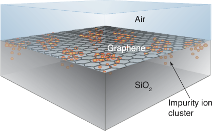
The simulated structure, shown in Figure 1, consists of a monolayer of graphene placed on a silicon-dioxide substrate that contains charged impurities. On the four vertical planes that bound the simulation domain perpendicular to the graphene layer, we apply periodic boundary conditions to the fields and carrier momenta. The top and bottom planes that bound the simulation domain parallel to the graphene layer are terminated using convolutional perfectly matched layer (CPML) absorbing boundary conditions Taflove and Hagness (2005). In the FDTD/MD electrodynamic solver, the monolayer of graphene is defined by one plane of grid points with a dielectric constant of , while the grid points above and below this plane are given dielectric constants of (air) and (SiO2), respectively.
We assume that the Fermi level and carrier density in graphene can be modulated by a back gate, located at the bottom of the SiO2 substrate. For a given Fermi level and temperature, the electron and hole densities are given by and , respectively.Fang et al. (2007) Here, , , and is the Fermi integral of order . is the tunable Fermi level and is the Fermi velocity in graphene on SiO2 Knox et al. (2008). The carrier ensemble in the 2D plane of graphene, comprising electrons and holes, is initialized by using random numbers to assign a position, momentum, charge, and spin to each carrier, taking into account the appropriate statistical probabilities. For the calculation of the grid-based charge density, carriers localized throughout the simulation domain are assigned to the grid using the cloud-in-cell method Laux (1996). The initial electric field distribution is calculated by solving Poisson’s equation using the successive-over-relaxation method Press (1989). We use the tight-binding Bloch wave functions Sule and Knezevic (2012) to calculate the electron-phonon scattering rates in graphene, accurately reproducing the rates from first-principles calculations Borysenko et al. (2010), and to compute the electron-surface-optical (SO) phonon scattering rates Konar et al. (2010). The scattering rates for holes are assumed to be the same as those for electrons. These initialization steps are followed by a time-stepping loop in which EMC and FDTD/MD source each other and which terminates once a steady state is achieved, as identified by the saturation of the ensemble-averaged carrier velocity and energy.
II.2 Generating Clustered Impurity Distributions in the Simulation
In order to capture the influence of charged impurities on electron and hole transport in graphene, we generate different impurity distributions throughout the SiO2 substrate. The type and charge of relevant impurities vary with the processing details Liang et al. (2011); for simplicity, we use generic impurity ions with unit positive charge. The impurity ions in the simulation are distributed in three dimensions (3D); however, impurities in the graphene literature are typically described via a cumulative sheet density, , in units of . For a generated 3D distribution of ions, the sheet density is obtained by integrating over a depth equal to , where represents the effective size of an impurity ion in the MD calculation (see Willis et al. Willis et al. (2011, 2013) for more details), followed by averaging over the total depth of the 3D distribution. is typically between and . We have observed that charged impurities placed deeper than do not significantly affect carrier transport for reasonable impurity sheet densities ().
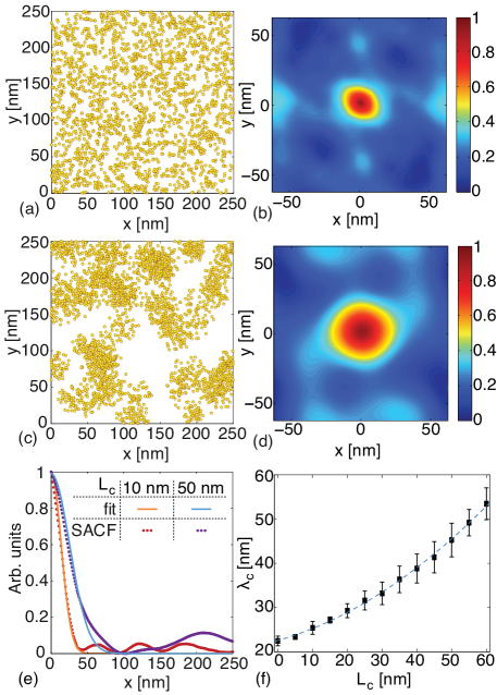
The problem of positioning individual impurities in 3D to achieve a predetermined cluster size distribution is related to 3D Voronoi tessellation Priolo et al. (1992); Fan et al. (2004); Ferenc and Néda (2007). Here, we have developed a relatively simple algorithm that enables us to generate an approximately Gaussian distribution of individual impurities starting from a single numerical parameter, , which we refer to as the clustering parameter. For , we distribute all the impurity ions stochastically according to a uniform random distribution. For a non-zero , we generate impurity clusters, where is the 2D area of the graphene layer in the simulation. To initialize the positions of individual impurities, we first distribute the centers of the clusters stochastically. Secondly, we pick the characteristic size of each individual cluster from a uniform random distribution between and , the average being . Next, we distribute individual impurity ions around each cluster center following a Gaussian distribution whose standard deviation equals half of the cluster size. Examples of clustered impurity distributions are shown in Figure 2a () and Figure 2c (), with the corresponding spatial autocorrelation functions (SACFs) depicted in Figures 2b and 2d, respectively. As shown in Figure 2e, normalized Gaussians (orange and blue curves) fit the SACFs (red and purple dots) well. Moreover, the full-width at half-maximum (FWHM) of the SACF agrees well with the correlation length extracted from the Gaussian fits. Henceforth, the FWHM of the impurity-distribution SACF will be referred to as the average impurity cluster size and denoted by . Figure 2f presents versus . Each data point in Figure 2f represents the average of fourteen slightly different impurity ion configurations obtained stochastically for a given value of (ranging from 0 to in the increments of ) and the error bars on the data points denote the standard deviations.
It is important to note that is conceptually different from the correlation length used by Li et al. Li et al. (2011) represents the extent to which impurity ions can interact with one another and diffuse; as a result, a larger results in an impurity distribution that is more spread out than clustered. In contrast, a larger (stemming from a larger , see Figure 2f) represents a more clustered distribution.
III Results and Discussion
III.1 Formation of electron–hole puddles
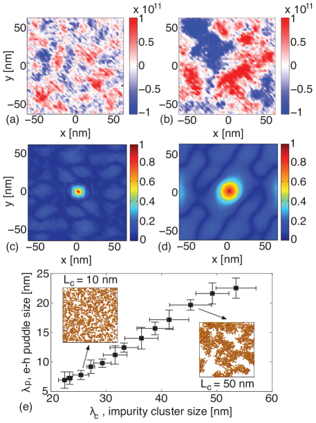
Figure 3 shows the formation of electron–hole puddles in the presence of clustered impurity distributions. We simulate carrier transport at room temperature, for the Fermi level at the Dirac point (), and without external fields. The initial positions of the charge carriers in the simulation are generated randomly based on a uniform spatial distribution and the calculated electron and hole sheet densities . As the simulation progresses, carriers move and scatter until a steady state is reached. The motion of carriers under the influence of the other charges in the domain (the clustered ions as well as other carriers) results in a charge redistribution and the formation of electron–hole puddles. The average electron–hole puddle size is estimated from the FWHM Rossi and Das Sarma (2008) of the SACF of the carrier density distribution. In Figures 3a and 3b, we contrast the carrier density distributions that stem from the underlying uniform random (, ) and clustered impurity distributions (, ). The corresponding SACFs of the carrier density are shown in Figs. 3c and 3d; the corresponding average electron–hole puddle sizes, estimated from the FWHM of these SACFs, are and , respectively. These examples show a very significant difference in the sizes of electron–hole puddles that result from random and clustered impurity ion distributions. Figure 3e shows the average electron–hole puddle size, , as a function of the average impurity cluster size . Different simulation runs for the same , , and produce slightly different puddle and impurity cluster sizes owing to the stochastic nature of the impurity position initialization and the EMC routine. Therefore, each data point in Figure 3e represents the average of fourteen simulations for a given value of (ranging from 0 to in the increments of ) and the error bars on the data points denote the standard deviations. A uniform random impurity distribution results in an average puddle size of only , while impurity clusters with an average size of 40–50 nm give rise to electron–hole puddles with an average size of , in agreement with experimental observations Deshpande et al. (2011); Xue et al. (2011); Zhang et al. (2009).
III.2 Role of impurity distribution in carrier transport. Residual conductivity
Next, we examine the effect of random and clustered impurity distributions on carrier transport in supported graphene. We calculate the conductivity, , as a function of electron density for various spatial formations and total sheet densities of impurity ions. The electron density is varied by varying the Fermi level, mimicking the effect of a back gate. An external dc electric field is applied in the plane of the graphene sheet. The field is introduced using a total-field scattered-field incident-wave source condition for a uniform plane wave with a half-Gaussian temporal variation Taflove and Hagness (2005); the magnitude of the source remains constant once the peak value is achieved. The conductivity is calculated from , where is the local electric field and is the current density. As and are noisy, we find in the steady state, upon averaging over position and time. In the following simulation results, we have used () for a uniform random and () for a clustered impurity distribution.
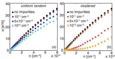
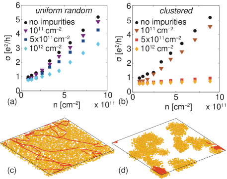
In Figure 4, we present for graphene on SiO2 at several impurity sheet densities, ranging from impurity-free to , with uniform random and clustered impurity distributions. At low impurity densities (), the carrier-density dependence of conductivity is nearly the same for the random and clustered impurity distributions, which is not surprising and agrees with the work of Li et al. Li et al. (2011): with few impurities present, their effect on transport is minor, while carrier interactions with phonons and other carriers dominate. In contrast, at impurity densities higher than , uniform random and clustered impurity distributions result in significantly different variations. The most significant difference is seen at low carrier densities, where the conductivity for randomly distributed impurities increases nearly linearly with increasing carrier density, while that for clustered impurities remains flat. The slow increase in the conductivity near the charge neutrality point has also been observed in experimental measurements Chen et al. (2008); Dean et al. (2010), notably for samples with considerable impurity contamination.
In Figures 5a and 5b, we zoom in on the low-density behavior of from Figure 4. The low-density limit of conductivity, , known as the residual conductivity, has been observed in experiment Chen et al. (2008) and attributed to charged impurity scattering Adam et al. (2007). Here, we see that the value of depends on the impurity sheet density and distribution, with higher impurity density and more clustered distributions resulting in a lower . We attribute the low- flattening of conductivity and the lower value of for clustered distributions to carrier trapping. Figures 5c and 5d depict the paths of sample carriers in graphene with underlying random and clustered substrate impurity distributions, respectively. A large impurity cluster effectively traps an electron, localizing the electron’s trajectory to the cluster vicinity and preventing it from participating in the current flow.
III.3 Sublinearity in and carrier-carrier interactions
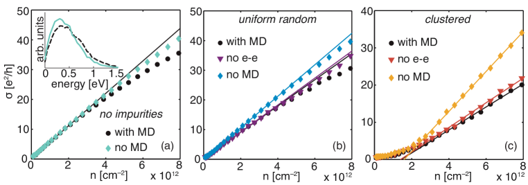
In Figure 6, we examine the role of short-range Coulomb interactions (carrier-carrier and carrier-ion) on dc transport in graphene on SiO2. We account for these effects via the MD part of the simulation and can selectively turn them on or off to better elucidate their importance. Figure 6a presents for impurity-free graphene, with MD (circles) and without MD (diamonds); without impurities, MD accounts only for the short-range, direct and exchange carrier-carrier interactions. We deduce that the sublinearity in at high carrier densities occurs largely due to carrier-carrier interactions: when we exclude their short-range component by turning off MD, becomes nearly linear. Any remaining sublinearity in the “no MD” results can be attributed to the long-range, direct carrier-carrier Coulomb interaction that is captured by the FDTD solver. Carrier-carrier Coulomb interactions do not directly affect conduction (the total momentum of an interacting pair is conserved, as is the pair’s total energy), but redistribute the momentum and energy among the pair and therefore affect the single-particle distribution function, pushing it towards a shifted Fermi-Dirac distribution Kriman et al. (1990); Lugli and Ferry (1986, 1985); Lundstrom (2000). The inset to Figure 6a presents the computed distribution of electrons over kinetic energy with and without carrier-carrier interaction for the electron density of (). This curve corresponds to , where is the electron density of states and is the distribution function, and carrier-carrier interaction clearly leads to a greater abundance of higher-energy carriers. Since electron and hole scattering rates with phonons increase with increasing energy, the redistribution of carriers over energy effectively raises the average carrier-phonon scattering rate and leads to a reduction in conductivity that we observe as the slopeover in .
In Figures 6b and 6c, we plot for uniform random and clustered impurity distributions with all short-range interactions accounted for through MD (circles, “with MD”), with short-range carrier-ion but without carrier-carrier interactions (triangles, “no e-e”), and without any short-range interactions (diamonds, “no MD”). We have already discussed the low-n region (see Figure 5) and will focus here on the medium-to-high electron density range. In both Figures 6b and 6c, the sheet density of impurities is appreciable (), so carrier-ion interactions govern transport in the medium and the dependence is largely linear Ando (2006). Turning off short-range carrier-carrier interactions causes insignificant change to the slope in either panel, while turning off short-range carrier-ion interactions significantly affects the slope.
III.4 Estimating impurity density from the inverse slope of
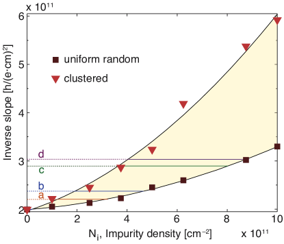
The slope of the curves in the linear region is governed by the short-range carrier-ion interactions, and is dependent on both the impurity density (Figure 4) and distribution (Figures 6b and 6c). As the slope can be accurately measured in experiment, we can use it to indirectly extract the impurity density and cluster size. In Figure 7, we present the EMC/FDTD/MD simulation results for the inverse slope of in the linear region as a function of the sheet impurity density, with the cluster size as a parameter. The solid markers represent the simulation results for uniform random (, , denoted by squares) and clustered impurity distributions (, , denoted by triangles). The curves are polynomial fits to guide the eye and indicate the range of results for different impurity distributions. As we discussed earlier, impurity cluster sizes of 40–50 nm correspond to electron–hole puddle sizes obtained in experiment(see Fig. 3), so it is likely that a reasonable sheet impurity density estimate can be obtained from the clustered impurity curve in Figure 7. As examples, we present the inverse slopes extracted from several room-temperature measurements on supported graphene (a – Ref. Vicarelli et al. (2012), b – Ref. Schedin et al. (2007), c – Ref. Novoselov et al. (2005), and d – Ref. Novoselov et al. (2004)). The intercepts of each inverse-slope horizontal line with the clustered and random distribution curves in Fig. 7 indicate an estimate of the impurity-density range, with the clustered-curve intercept likely yielding a good approximate value for . Note that the more recent experiments (a from 2012 Vicarelli et al. (2012) and b from 2007 Schedin et al. (2007)), which arguably had samples with fewer impurities than the early ones owing to the advances in processing, indeed correspond to lower sheet impurity densities than the earlier measurements (c in 2005 Novoselov et al. (2005) and d in 2004 Novoselov et al. (2004)).
IV CONCLUSION
In summary, we have employed EMC/FDTD/MD coupled simulation of carrier transport and electrodynamics to investigate the effects of carrier-carrier and carrier-ion Coulomb interactions on the transport properties of graphene on SiO2, with focus on the role of substrate impurity clustering. While corrections due to many-particle correlations Martin et al. (2008) and coherent transport features Young and Kim (2009); Mucciolo and Lewenkopf (2010) may play an important role in extremely clean suspended graphene at low temperatures, our simulations accurately capture the physics of diffusive, room-temperature carrier transport in supported graphene, which is relevant for device applications. We have shown that clustered impurity distributions with an average cluster size of 40–50 nm result in the formation of electron–hole puddles with a typical size of , comparable to observed values. We have also demonstrated that high-density clustered impurities lead to carrier trapping and a flattening of the low- dependence. By selectively controlling the short-range Coulomb interactions of the carriers in the coupled EMC/FDTD/MD simulation, we have shown that the sublinear dependence at high carrier densities can be attributed to carrier-carrier interactions Chen et al. (2008); Dean et al. (2010). The slope of the linear-region relates to the strength of the carrier-ion Coulomb interactions, and we have characterized its dependence on the impurity density and distribution. The computed dependence of the linear-region slope of on the impurity density might be used as a noninvasive technique for estimating the impurity density in experiment.
Acknowledgment
This work has been primarily supported by AFOSR, award No. FA9550-11-1-0299. I.K. acknowledges partial support by NSF, award No. 1201311.
References
- Castro Neto et al. (2009) A. H. Castro Neto, F. Guinea, N. M. R. Peres, K. S. Novoselov, and A. K. Geim, Rev. Mod. Phys. 81, 109 (2009).
- Das Sarma et al. (2011) S. Das Sarma, S. Adam, E. H. Hwang, and E. Rossi, Rev. Mod. Phys. 83, 407 (2011).
- Avouris (2010) P. Avouris, Nano Lett. 10, 4285 (2010).
- Young and Kim (2011) A. F. Young and P. Kim, Annu. Rev. Cond. Mat. Phys. 2, 101 (2011).
- Schwierz (2010) F. Schwierz, Nat. Nano 5, 487 (2010).
- Bonaccorso et al. (2010) F. Bonaccorso, Z. Sun, T. Hasan, and A. C. Ferrari, Nat. Photon. 4, 611 (2010).
- Kim et al. (2009) K. S. Kim, Y. Zhao, H. Jang, S. Y. Lee, J. M. Kim, K. S. Kim, J.-H. Ahn, P. Kim, J.-Y. Choi, and B. H. Hong, Nature 457, 706 (2009).
- Kim et al. (2010) B. J. Kim, H. Jang, S.-K. Lee, B. H. Hong, J.-H. Ahn, and J. H. Cho, Nano Lett. 10, 3464 (2010).
- Lin et al. (2010) Y.-M. Lin, C. Dimitrakopoulos, K. A. Jenkins, D. B. Farmer, H.-Y. Chiu, A. Grill, and P. Avouris, Science 327, 662 (2010).
- Sensale-Rodriguez et al. (2012) B. Sensale-Rodriguez, R. Yan, M. M. Kelly, T. Fang, K. Tahy, W. S. Hwang, D. Jena, L. Liu, and H. G. Xing, Nat. Commun. 3, 780 (2012).
- Otsuji et al. (2012) T. Otsuji, S. A. B. Tombet, A. Satou, H. Fukidome, M. Suemitsu, E. Sano, V. Popov, M. Ryzhii, and V. Ryzhii, J. Phys. D: Appl. Phys. 45, 303001 (2012).
- Schedin et al. (2007) F. Schedin, A. K. Geim, S. V. Morozov, E. W. Hill, P. Blake, M. I. Katsnelson, and K. S. Novoselov, Nat. Mater. 6, 652 (2007).
- Pumera (2011) M. Pumera, Mater. Today 14, 308 (2011).
- Yu et al. (2008) Q. Yu, J. Lian, S. Siriponglert, H. Li, Y. P. Chen, and S.-S. Pei, Appl. Phys. Lett. 93, 113103 (2008).
- Li et al. (2009) X. Li, W. Cai, J. An, S. Kim, J. Nah, D. Yang, R. Piner, A. Velamakanni, I. Jung, E. Tutuc, S. K. Banerjee, L. Colombo, and R. S. Ruoff, Science 324, 1312 (2009).
- Meyer et al. (2007) J. C. Meyer, A. Geim, M. Katsnelson, K. Novoselov, T. Booth, and S. Roth, Nature 446, 60 (2007).
- Lin et al. (2012) Y.-C. Lin, C.-C. Lu, C.-H. Yeh, C. Jin, K. Suenaga, and P.-W. Chiu, Nano Lett. 12, 414 (2012).
- Casiraghi et al. (2007) C. Casiraghi, S. Pisana, K. Novoselov, A. Geim, and A. Ferrari, Appl. Phys. Lett. 91, 233108 (2007).
- Martin et al. (2008) J. Martin, N. Akerman, G. Ulbricht, T. Lohmann, J. H. Smet, K. von Klitzing, and A. Yacoby, Nat. Phys. 4, 144 (2008).
- Zhang et al. (2009) Y. Zhang, V. W. Brar, C. Girit, A. Zettl, and M. F. Crommie, Nat. Phys. 5, 722 (2009).
- Rossi and Das Sarma (2008) E. Rossi and S. Das Sarma, Phys. Rev. Lett. 101, 166803 (2008).
- Adam et al. (2007) S. Adam, E. H. Hwang, V. M. Galitski, and S. Das Sarma, Proc. Natl. Acad. Sci USA 104, 18392 (2007).
- Deshpande et al. (2011) A. Deshpande, W. Bao, Z. Zhao, C. N. Lau, and B. J. LeRoy, Phys. Rev. B 83, 155409 (2011).
- McCreary et al. (2010) K. McCreary, K. Pi, A. Swartz, W. Han, W. Bao, C. Lau, F. Guinea, M. Katsnelson, and R. Kawakami, Phys. Rev. B 81, 115453 (2010).
- Ando (2006) T. Ando, J. Phys. Soc. Jpn. 75, 074716 (2006).
- Hwang et al. (2007) E. H. Hwang, S. Adam, and S. Das Sarma, Phys. Rev. Lett. 98, 186806 (2007).
- Chen et al. (2008) J. H. Chen, C. Jang, S. Adam, M. S. Fuhrer, E. D. Williams, and M. Ishigami, Nat. Phys. 4, 377 (2008).
- Dean et al. (2010) C. R. Dean, A. F. Young, I. Meric, C. Lee, L. Wang, S. Sorgenfrei, K. Watanabe, T. Taniguchi, P. Kim, K. L. Shepard, and J. Hone, Nature Nanotechnology 5, 722 (2010).
- Tan et al. (2007) Y.-W. Tan, Y. Zhang, K. Bolotin, Y. Zhao, S. Adam, E. Hwang, S. D. Sarma, H. Stormer, and P. Kim, Phys. Rev. Lett. 99, 246803 (2007).
- Wehling et al. (2010) T. Wehling, S. Yuan, A. Lichtenstein, A. Geim, and M. Katsnelson, Phys. Rev. Lett. 105, 056802 (2010).
- Li et al. (2011) Q. Li, E. H. Hwang, E. Rossi, and S. Das Sarma, Phys. Rev. Lett. 107, 156601 (2011).
- Radchenko et al. (2012) T. Radchenko, A. Shylau, and I. Zozoulenko, Phys. Rev. B 86, 035418 (2012).
- Xue et al. (2011) J. Xue, J. Sanchez-Yamagishi, D. Bulmash, P. Jacquod, A. Deshpande, K. Watanabe, T. Taniguchi, P. Jarillo-Herrero, and B. J. LeRoy, Nat. Mater. 10, 282 (2011).
- Jang et al. (2008) C. Jang, S. Adam, J.-H. Chen, E. D. Williams, S. Das Sarma, and M. S. Fuhrer, Phys. Rev. Lett. 101, 146805 (2008).
- Kohn and Luttinger (1957) W. Kohn and J. M. Luttinger, Phys. Rev. 108, 590 (1957).
- Rossi et al. (2009) E. Rossi, S. Adam, and S. Das Sarma, Phys. Rev. B 79, 245423 (2009).
- Adam et al. (2009) S. Adam, E. Hwang, E. Rossi, and S. D. Sarma, Solid State Communications 149, 1072 (2009), recent Progress in Graphene Studies.
- Willis et al. (2011) K. J. Willis, S. C. Hagness, and I. Knezevic, J. Appl. Phys. 110, 063714 (2011).
- Sule et al. (2013) N. Sule, K. J. Willis, S. C. Hagness, and I. Knezevic, J. Comput. Electron. (2013), published online, DOI: 10.1007/s10825-013-0508-1.
- Willis et al. (2013) K. J. Willis, S. C. Hagness, and I. Knezevic, Appl. Phys. Lett. 102, 122113 (2013).
- Jacoboni and Reggiani (1983) C. Jacoboni and L. Reggiani, Rev. Mod. Phys. 55, 645 (1983).
- Taflove and Hagness (2005) A. Taflove and S. Hagness, Computational Electrodynamics: The Finite-Difference Time-Domain Method (Artech House, 2005).
- Yee (1966) K. Yee, IEEE T. Antenn. Propag. 14, 302 (1966).
- Fischetti and Laux (2001) M. V. Fischetti and S. E. Laux, J. Appl. Phys. 89, 1205 (2001).
- Joshi and Ferry (1991) R. P. Joshi and D. K. Ferry, Phys. Rev. B 43, 9734 (1991).
- Rapaport (2004) D. Rapaport, The Art of Molecular Dynamics Simulation (Cambridge University Press, 2004).
- Fang et al. (2007) T. Fang, A. Konar, H. Xing, and D. Jena, Appl. Phys. Lett. 91, 092109 (2007).
- Knox et al. (2008) K. R. Knox, S. Wang, A. Morgante, D. Cvetko, A. Locatelli, T. O. Mentes, M. A. Niño, P. Kim, and R. M. Osgood, Phys. Rev. B 78, 201408 (2008).
- Laux (1996) S. Laux, IEEE Trans. Comput-Aided Des. Integr. Circuits Syst. 15, 1266 (1996).
- Press (1989) W. H. Press, Numerical recipes : the art of scientific computing (Cambridge University Press, New York, N.Y., 1989).
- Sule and Knezevic (2012) N. Sule and I. Knezevic, J. Appl. Phys. 112, 053702 (2012).
- Borysenko et al. (2010) K. M. Borysenko, J. T. Mullen, E. A. Barry, S. Paul, Y. G. Semenov, J. M. Zavada, M. B. Nardelli, and K. W. Kim, Phys. Rev. B 81, 121412 (2010).
- Konar et al. (2010) A. Konar, T. Fang, and D. Jena, Phys. Rev. B 82, 115452 (2010).
- Liang et al. (2011) X. Liang, B. A. Sperling, I. Calizo, G. Cheng, C. A. Hacker, Q. Zhang, Y. Obeng, K. Yan, H. Peng, Q. Li, X. Zhu, H. Yuan, A. R. Hight Walker, Z. Liu, L.-m. Peng, and C. A. Richter, ACS Nano 5, 9144 (2011).
- Priolo et al. (1992) A. Priolo, H. M. Jaeger, A. J. Dammers, and S. Radelaar, Phys. Rev. B 46, 14889 (1992).
- Fan et al. (2004) Z. Fan, Y. Wu, X. Zhao, and Y. Lu, Comp. Mat. Sci. 29, 301 (2004).
- Ferenc and Néda (2007) J.-S. Ferenc and Z. Néda, Physica A 385, 518 (2007).
- Kriman et al. (1990) A. M. Kriman, M. J. Kann, D. K. Ferry, and R. Joshi, Phys. Rev. Lett. 65, 1619 (1990).
- Lugli and Ferry (1986) P. Lugli and D. K. Ferry, Phys. Rev. Lett. 56, 1295 (1986).
- Lugli and Ferry (1985) P. Lugli and D. K. Ferry, IEEE Trans. Electron Devices 32, 2431 (1985).
- Lundstrom (2000) M. Lundstrom, Fundamentals of Carrier Transport (Cambridge University Press, Cambridge, UK, 2000).
- Vicarelli et al. (2012) L. Vicarelli, M. S. Vitiello, D. Coquillat, A. Lombardo, A. C. Ferrari, W. Knap, M. Polini, V. Pellegrini, and A. Tredicucci, Nat. Mater. 11, 865 (2012).
- Novoselov et al. (2005) K. S. Novoselov, D. Jiang, F. Schedin, T. J. Booth, V. V. Khotkevich, S. V. Morozov, and A. K. Geim, Proc. Natl. Acad. Sci. U.S.A. 102, 10451 (2005).
- Novoselov et al. (2004) K. S. Novoselov, A. K. Geim, S. V. Morozov, D. Jiang, Y. Zhang, S. V. Dubonos, I. V. Grigorieva, and A. A. Firsov, Science 306, 666 (2004).
- Young and Kim (2009) A. F. Young and P. Kim, Nature Phys. 5, 222 (2009).
- Mucciolo and Lewenkopf (2010) E. R. Mucciolo and C. H. Lewenkopf, J. Phys.: Condens. Matter 22, 273201 (2010).