On-Chip Detection of Entangled Photons by Scalable Integration of Single-Photon Detectors
Photonic integrated circuits (PICs) have emerged as a scalable platform for complex quantum technologies using photonic and atomic systems Aspuru-Guzik and Walther (2012); O’Brien et al. (2009); Amini et al. (2010). A central goal has been to integrate photon-resolving detectors to reduce optical losses, latency, and wiring complexity associated with off-chip detectors. Superconducting nanowire single-photon detectors (SNSPDs Gol’tsman et al. (2001); Hadfield (2009)) are particularly attractive because of high detection efficiency Marsili et al. (2013), sub-50-ps timing jitter (Dauler et al., 2009), nanosecond-scale reset time Marsili et al. (2012a), and sensitivity from the visible to the mid-infrared spectrum Marsili et al. (2012b). However, while single SNSPDs have been incorporated into individual waveguides Sprengers et al. (2011); Pernice et al. (2012), the system efficiency of multiple SNSPDs in one photonic circuit has been limited below 0.2% (Sahin et al., 2013; Heeres et al., 2013) due to low device yield Kerman et al. (2007). Here we introduce a micrometer-scale flip-chip process that enables scalable integration of SNSPDs on a range of PICs. Ten low-jitter detectors were integrated on one PIC with 100% device yield. With an average system efficiency beyond 10% for multiple SNSPDs on one PIC, we demonstrate high-fidelity on-chip photon correlation measurements of nonclassical light.
Photonic integrated circuits are being developed for a wide range of applications in quantum information science, including quantum simulation(Spring et al., 2013; Broome et al., 2013; Aspuru-Guzik and Walther, 2012; Aaronson and Arkhipov, 2011), quantum photonic state generation Silverstone et al. (2014); Chen et al. (2011); Fukuda et al. (2005); Mower and Englund (2011), quantum-limited detection Guha and Erkmen (2009), and linear optical quantum computingPoliti et al. (2008); O’Brien et al. (2009); Nielsen (2004); Knill et al. (2001). These applications require multiple detectors with low timing jitter. The lowest timing jitter for infrared photon detection has been achieved with SNSPDs based on sub-100-nm-wide and 4-nm-thick niobium nitride (NbN) nanowires. However, to date there has been no scalable approach to integration of SNSPDs into photonic circuits: while single isolated waveguide-integrated SNSPDs have been demonstrated Sprengers et al. (2011); Pernice et al. (2012), the highest reported system detection efficiency for just two SNSPDs integrated into the same photonic circuit remains significantly below 1% (Sahin et al., 2013; Heeres et al., 2013). The central challenge when building systems with multiple SNSPDs remains the low fabrication yield, which is limited by defects at the nanoscale Kerman et al. (2007). This yield problem is exacerbated when such detectors are integrated onto photonic chips, which can require tens of additional fabrication steps of their own. Here we report on a micrometer-scale flip-chip process developed to overcome the yield problem by separating the PIC and the SNSPD fabrication processes. Our approach is compatible with a wide range of PICs, including CMOS-compatible silicon photonics, in a back-end-of-the-line step.
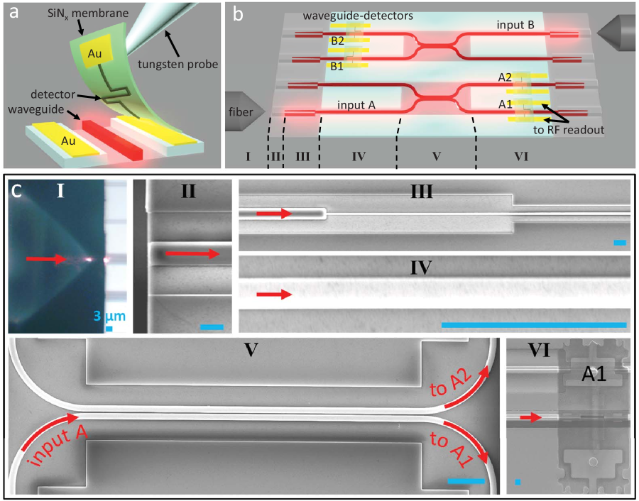
Fig. 1(a) outlines the elements of the assembly process. Hairpin-shaped SNSPDs (Sprengers et al., 2011; Pernice et al., 2012) were fabricated on 200-nm-thick silicon nitride (SiNx) membranes; silicon-on-oxide (SOI) PICs were fabricated separately (see Methods). After evaluating the SNSPDs in a cryostat, high-performance detectors were selected from the fabrication chip and transferred onto the desired SOI waveguides. Using this method, we assembled a proof-of-concept photonic circuit, shown in Fig. 1(b), comprising an optical network with two input and four output ports, each coupled to an SNSPD. We measured an estimated on-chip detection efficiency up to 45% for 1550-nm-wavelength single photons and timing jitter as low as 42 ps. The light was coupled into the waveguides using inverse tapered couplers with 3 dB insertion loss McNab et al. (2003), resulting in a system detection efficiency (from the external fiber) up to . This system efficiency enables the first on-chip intensity autocorrelation measurements of nonclassical light, demonstrated here for photon pairs generated by spontaneous parametric down conversion.

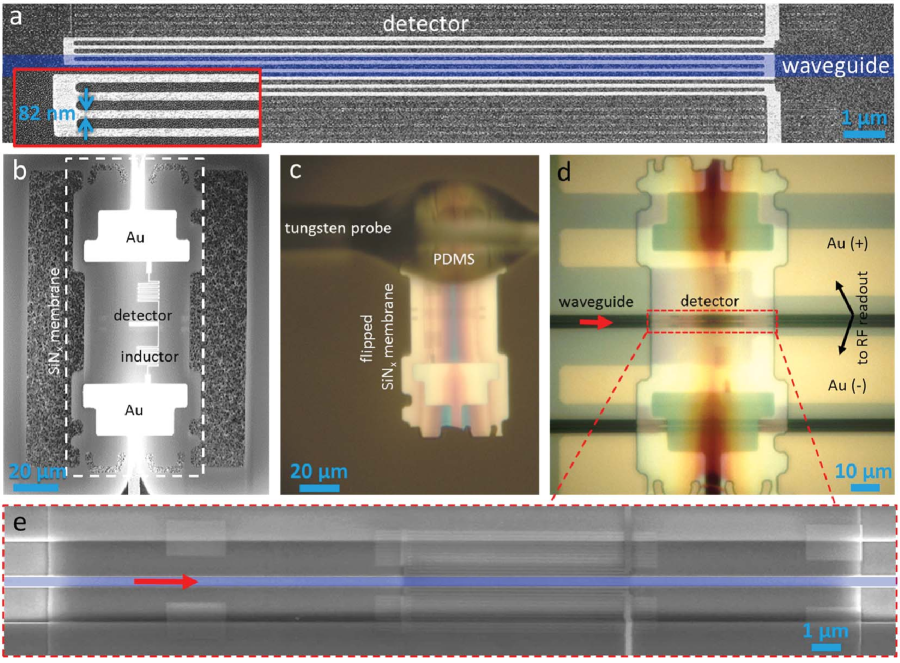
The detector comprised multiple nanowires connected in parallel (see SI), as shown in Fig. 2(a). This SNSPD variant Ejrnaes et al. (2007); Marsili et al. (2011) has been shown to double the signal-to-noise ratio of the photodetection voltage compared to traditional single-wire SNSPDs. The detector length was designed using a finite-element model (Hu et al., 2009) to ensure optical absorption exceeding 50% (see SI).
We fabricated 225 detectors on a 200-nm-thick SiNx layer over a Si substrate. The underlying silicon was then etched (see Methods), leaving hundreds of free-standing membranes carrying SNSPDs. One of these suspended membranes is shown in Fig. 2(b). Each membrane was connected to the bulk substrate through six narrow ( 2-m-wide) bridges, two of which connected the detector on the membrane electrically to large contact pads on the bulk substrate for testing the detectors after the etch step (see SI).
We characterized all detectors to identify low-jitter, high-efficiency devices (typically about 30% of the detectors). As shown in Fig. 2(c), we removed selected detector membranes from the substrate using tungsten microprobes coated with polydimethylsiloxane (PDMS) adhesive. We then placed membranes detector-side-down onto the target waveguide with sub-1-m alignment accuracy under an optical microscope. For electrical readout, the gold pads on the membranes contacted complementary pads on the PIC (Fig. 2(d)). These gold-gold contacts withstood repeated thermal cycles with no noticeable degradation (see SI). Fig. 2(e) shows the resulting waveguide-integrated detector. Because we transferred only high-performance detectors, we were able to achieve perfect yield in the assembled device, resolving the non-scalability of low-jitter SNSPD fabrication Kerman et al. (2007).

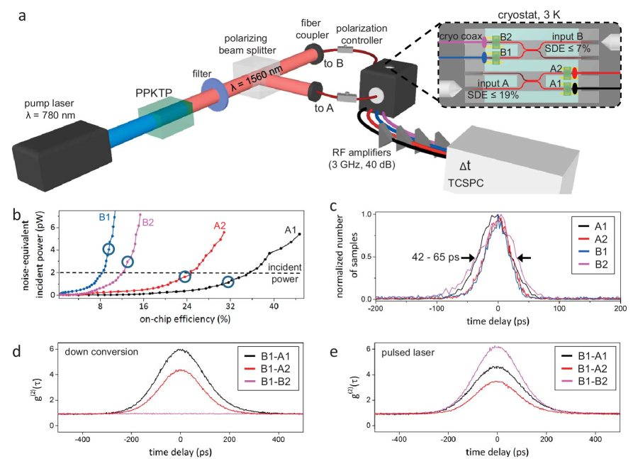
Using this process, we integrated four detectors (labeled A1, A2, B1 and B2) on a PIC and characterized the performance of the PIC shown in Figs. 1(b,c) using four parameters: system detection efficiency (SDE), on-chip detection efficiency (ODE), FWHM timing jitter (TJ), and noise-equivalent incident power (NEIP). The SDE includes all losses (i.e., coupling and transmission) between the fiber port outside the cryostat and the detector. We determined the SDE from the ratio of the SNSPD photocount rate to the photon flux coupled into the fiber port (see SI). Our chip reached an SDE of 19% for input A (11% for A1 and 8% for A2) and 7% for input B (3% for B1 and 4% B2). These SDE values represent an improvement of two orders of magnitude compared to previous approaches for multi-detector integration Sahin et al. (2013).
The ODE is defined as the probability that a photon already coupled into the waveguide is detected Pernice et al. (2012); Sahin et al. (2013) (see SI). We estimated the ODE as SDE/, where accounts for coupling losses into the PIC (3 dB) and the splitting ratio of the directional couplers before the SNSDPs (3 dB). The transferred detectors reached ODEs between 12% and 45% and 42- to 65-ps TJ.
The NEIP is given by , where SDCR is the system dark count rate and eV. Fig. 3(b) shows the NEIP vs. ODE for the waveguide detectors on couplers A and B. The ratio of the power incident onto the detectors (IP) and the NEIP characterizes the signal-to-noise ratio for single-shot measurements. In this work, the NEIP was limited by radiation leakage (see SI) through a cryostat window used to image and align the lensed fibers to the polymer couplers (Fig. 1(c-I)). Hence, for subsequent measurements, we operated the detectors at lower ODEs of 10 - 32% (circled points in Fig. 3(b)), which reduced the dark count rate and resulted in a ratio of IP/NEIP 0.5 - 1.7.
We used these high-SDE SNSPDs to characterize time-energy entangled photon pairs entirely on the PIC. Entangled photon pairs were generated by spontaneous parametric down conversion (SPDC) from a 1-cm periodically poled potassium titanyl phosphate (PPKTP) waveguide, as shown in Fig. 3(a). Signal and idler photons of 1 ps duration and orthogonal polarization were separated using a polarizing beam splitter and sent into inputs A and B of the PIC. The SPDC pump power was adjusted to generate pairs at Hz, corresponding to a multi-pair probability of per TJ. We obtained the second-order correlation function from , where is the measured number of coincidences between inputs A and B at time difference , () is the count rate from input A (B), is the coincidence bin duration, and is the integration time. Fig. 3(d) shows the resulting function. Photon bunching is evident between inputs A and B, but not within individual channels (i.e., between A1 and A2 or B1 and B2), as expected for an entangled photon source. The observed peak heights of and are lower than the theoretical value for ideal detectors due to the finite IP/NEIP ratio of our detectors (see Methods). By contrast, when pulses from a mode-locked laser were injected into inputs A and B with average photon number per pulse greater than one, bunching was observed between all detector pairs (Fig. 3(e)), as expected for a pulsed classical source.

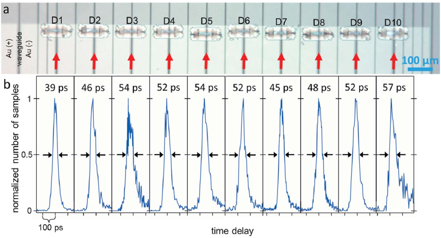
The ability to pre-select functioning devices enables scaling to more detectors with unity yield. Fig. 4(a) shows ten SNSPDs (D1-10) on adjacent waveguides with TJ values of 39 ps - 57 ps for 1550-nm-wavelength light. For rapid characterization, these devices were measured by top illumination in a cryogenic probe station. The photodetection delay histograms for all detectors are shown in Fig. 4(b).

The membrane transfer demonstrated here could be used to integrate other electro-optic devices, such as III-V lasers or single-photon sources, onto PICs. Since the device membrane is flexible, it conforms to the target chip, even if that chip is not perfectly flat. Because of the small size of the membrane, the process is also relatively tolerant to defects on the target chip, as opposed to processes involving large-area flip-chip bonding (e.g., see Ref. Fang et al. (2006)), which require both surfaces to be free of defects.
In conclusion, we have demonstrated the scalable integration of high-performance SNSPDs into photonic integrated circuits. We assembled ten adjacent waveguide-integrated detectors on a silicon PIC with 100% yield and observed detector timing jitter values between 39 and 57 ps. Waveguide-integrated SNSPDs on the same PIC enabled on-chip -measurements of nonclassical light. Scaling to many tens to hundreds of detectors would ultimately be limited by the readout complexity. There is ongoing work to address this problem using electrical multiplexing schemes Zhao et al. (2013). For more detectors, which require greater bandwidth, optical wavelength division multiplexing could be used, employing high-speed ( GHz) modulators already available on PICsThomson et al. (2012). The integration process demonstrated here is CMOS compatible; indeed, the PICs used in this experiment were fabricated in a CMOS compatible process with the exception of the polymer waveguide couplers, which can be replaced with SiNxShani et al. (1989). Thus, it appears likely that tens to hundreds of SNSPDs and other heterogeneous circuit elements can be integrated into high-performance PICs. This demonstration opens the door to fully integrated, high-performance photonic processors for quantum information science.
Methods
Detector fabrication. A 200-nm-thick SiNx layer was grown via plasma-enhanced chemical vapor deposition (PECVD) on double-polished silicon substrates. The NbN film was deposited on top of the SiNx layer via reactive magnetron sputtering (AJA system) at a substrate holder temperature of 800 ∘C. The sheet resistance of the 4-nm-thick NbN films (thickness estimated from the deposition time) was 515 /square and the critical temperature was 10.9 K. Electrical contact pads were defined by UV-exposing a 700-nm-thick PMGI layer covered with 1.5-m-thick photoresist (S1813) for 13 seconds at 2300 W/cm2 and developing the bilayer for 24 seconds in CD-26. This process achieved an undercut of the photoresist by 2 m, enabling smooth gold pad edges after liftoff. 10 nm Ti and 15 nm Au were evaporated and the liftoff was performed in acetone under sonication for 2 minutes followed by a 1-min dip in CD-26 and a 1-min DI dip. 70-nm-thick electron-beam-resist (HSQ) was spun on top of the sample, exposed in a 30 keV electron beam lithography tool (Raith 150, exposure dose 700-850 C/cm2) and developed in TMAH at 27 ∘C for 3 minutes. The HSQ pattern was transferred into NbN via a 2.5-min CF4 reactive-ion etch (RIE) at 50 W. In order to improve electron-beam dose uniformity Yang et al. (2005), additional features were exposed outside the hairpin-shaped detector. These dummy structures, also referred to as proximity-effect-correction features, are shown as parallel lines in dark grey outside the detector in Fig. 2(a).
Detector suspension. The detector was covered with S1813 and a trench pattern was exposed in the photoresist. This pattern was then used as an etch mask to define trenches around the detector through the SiNx layer via RIE with CF4. This trench pattern left the underlying silicon substrate exposed. The silicon under the SiNx layer was removed using XeF2, a selective isotropic etch gas. In the final step, the photoresist was removed in an NMP solution (see SI), resulting in a detector on a suspended SiNx membrane.
PIC fabrication. The PIC was fabricated on a 10 -cm, p-doped, 200-mm silicon-on-insulator (SOI) wafer from SOITEC. The wafer had a 220-nm-thick silicon device layer on top of a 2 m buried oxide layer. The 500-nm-wide silicon waveguides were fabricated on a CMOS line at the IBM Watson Research Center using electron-beam lithography. In a subsequent optical lithography step, SU8 polymer couplers were fabricated to allow sub-3-dB coupling loss from a lensed fiber to the silicon waveguide (see Ref. Vlasov and McNab (2004) for further details). The gold pads on the PIC were fabricated in a similar manner to that outlined in the detector fabrication section above.
Timing jitter measurements. We used a mode-locked, sub-ps-pulse-width laser emitting at 1550 nm wavelength and 38 MHz repetition rate. The laser output was split into two SMF28 fibers, which we coupled to the detector under test and to a low-timing-jitter photodiode. The light coupled to the detector was attenuated to 5 pW and operation of the detector in single-photon regime was checked by confirming the linearity of the photocount rate as a function of incident photon flux (see SI). For detectors A1, A2, B1 and B2 the light was coupled to the waveguides A and B using a lensed fiber as shown in Fig. 1(b) and Fig. 1(c-I). The second sample, containing detectors D1-10, was back-illuminated with a high-NA fiber with light from the mode-locked laser, and single-photon operation regime was confirmed as described above. The electrical output from the detector and from the photodiode were sent to a 6-GHz-bandwidth, 40-GSamples/s oscilloscope. We measured time delay between the detector pulse (start signal) and the pulse from the fast photodiode (stop signal). We acquired the instrument response function (IRF), a histogram of samples of , and measured the timing jitter of the detector, which was defined as the FWHM of the IRF.
Correlation measurements. can be calculated from experimental data using the formula given in the main text. To incorporate detector dark counts, we define rates , where (for channels and , respectively) and (corresponding to a ‘photon’ and ‘dark count,’ respectively). , for example, is the rate at which channel A registers dark counts, and is the count rate on channel A. Now is
| (1) |
where is the probability that channel B registers a photon given that channel A also registers a photon (i.e. the heralding efficiency) and is the bin duration. For and the ratio ,
| (2) |
In our experiment, , which gives an estimate of the heralding efficiency, .
Acknowledgements.
This work was supported by DARPA Information in a Photon program, through grant W911NF-10-1-0416 from the Army Research Office, and the NSF (grant ECCS-0823778). F. Najafi was supported by the Claude E. Shannon Fellowship. J. Mower and A. Dane were supported by the iQuISE fellowship. D.E. was supported in part by an IBM Faculty Award. The authors thank J. Daley, M. Mondol, L. Li, K. Sunter, Y. Ivry, X. Hu, A. McCaughan, Q. Zhao, AttoCube and Montana Instruments for technical support.Author Contributions
F.N., J.M., S.A., K.B. and D.E. conceived and designed the experiments. F.N., F.B., J.M., F.M., D.E. and K.B. designed the detectors. F.N. and A.D. fabricated the detectors. J.M., S.A. and D.E. developed the waveguide chip. C.L. and J.M. developed the SPDC source. F.N. and J.M. performed the experiments. N.H., J.M., P.K. and D.E. developed the membrane transfer process. N.H. performed the membrane transfer. F.N., J.M., N.H., K.B. and D.E. prepared the manuscript.
References
- Aspuru-Guzik and Walther (2012) A. Aspuru-Guzik and P. Walther, Nat Phys 8, 285 (2012).
- O’Brien et al. (2009) J. L. O’Brien, A. Furusawa, and J. Vuckovic, Nature Photonics 3, 687 (2009).
- Amini et al. (2010) J. M. Amini, H. Uys, J. H. Wesenberg, S. Seidelin, J. Britton, J. J. Bollinger, D. Leibfried, C. Ospelkaus, A. P. VanDevender, and D. J. Wineland, New Journal of Physics 12, 033031 (2010).
- Gol’tsman et al. (2001) G. N. Gol’tsman, O. Okunev, G. Chulkova, A. Lipatov, A. Semenov, K. Smirnov, B. Voronov, A. Dzardanov, C. Williams, and R. Sobolewski, Applied Physics Letters 79, 705 (2001).
- Hadfield (2009) R. Hadfield, Nature Photonics 3, 696 (2009).
- Marsili et al. (2013) F. Marsili, V. B. Verma, J. Stern, S. Harrington, A. Lita, T. Gerrits, I. Vayshenker, B. Baek, M. Shaw, R. Mirin, and S. W. Nam, Nat Photon 7, 210 (2013).
- Dauler et al. (2009) E. A. Dauler, A. J. Kerman, B. S. Robinson, J. K. Yang, B. Voronov, G. Goltsman, S. A. Hamilton, and K. K. Berggren, Journal of Modern Optics 56, 364 (2009).
- Marsili et al. (2012a) F. Marsili, F. Najafi, E. Dauler, R. J. Molnar, and K. K. Berggren, Applied Physics Letters 100, 112601 (2012a).
- Marsili et al. (2012b) F. Marsili, F. Bellei, F. Najafi, A. E. Dane, E. A. Dauler, R. J. Molnar, and K. K. Berggren, Nano Letters 12, 4799 (2012b), http://pubs.acs.org/doi/pdf/10.1021/nl302245n .
- Sprengers et al. (2011) J. P. Sprengers, A. Gaggero, D. Sahin, S. Jahanmirinejad, G. Frucci, F. Mattioli, R. Leoni, J. Beetz, M. Lermer, M. Kamp, S. Höfling, R. Sanjines, and A. Fiore, Applied Physics Letters 99, 181110 (2011).
- Pernice et al. (2012) W. Pernice, C. Schuck, O. Minaeva, M. Li, G. N. Goltsman, A. V. Sergienko, and H. X. Tang, Nature Communications 3, 1325 (2012).
- Sahin et al. (2013) D. Sahin, A. Gaggero, T. B. Hoang, G. Frucci, F. Mattioli, R. Leoni, J. Beetz, M. Lermer, M. Kamp, S. Höfling, and A. Fiore, Opt. Express 21, 11162 (2013).
- Heeres et al. (2013) R. Heeres, L. Kouwenhoven, and V. Zwiller, Nature Nanotechnology 8, 719 (2013).
- Kerman et al. (2007) A. J. Kerman, E. A. Dauler, J. K. W. Yang, K. M. Rosfjord, V. Anant, K. K. Berggren, G. N. Gol’tsman, and B. M. Voronov, Applied Physics Letters 90, 101110 (2007).
- Spring et al. (2013) J. B. Spring, B. J. Metcalf, P. C. Humphreys, W. S. Kolthammer, X.-M. Jin, M. Barbieri, A. Datta, N. Thomas-Peter, N. K. Langford, D. Kundys, J. C. Gates, B. J. Smith, P. G. R. Smith, and I. A. Walmsley, Science 339, 798 (2013), http://www.sciencemag.org/content/339/6121/798.full.pdf .
- Broome et al. (2013) M. A. Broome, A. Fedrizzi, S. Rahimi-Keshari, J. Dove, S. Aaronson, T. C. Ralph, and A. G. White, Science 339, 794 (2013), http://www.sciencemag.org/content/339/6121/794.full.pdf .
- Aaronson and Arkhipov (2011) S. Aaronson and A. Arkhipov, in Proceedings of the 43rd annual ACM symposium on Theory of computing, STOC ’11 (ACM, New York, NY, USA, 2011) pp. 333–342.
- Silverstone et al. (2014) J. Silverstone, W. D. Bonneau, K. Ohira, N. Suzuki, H. Yoshida, N. Iizuka, M. Ezaki, C. M. Natarajan, M. G. Tanner, R. H. Hadfield, V. Zwiller, G. D. Marshall, J. G. Rarity, J. L. O’Brien, and M. G. Thompson, Nat Photon 8, 104 (2014).
- Chen et al. (2011) J. Chen, Z. H. Levine, J. Fan, and A. L. Migdall, Opt. Express 19, 1470 (2011).
- Fukuda et al. (2005) H. Fukuda, K. Yamada, T. Shoji, M. Takahashi, T. Tsuchizawa, T. Watanabe, J. ichi Takahashi, and S. ichi Itabashi, Opt. Express 13, 4629 (2005).
- Mower and Englund (2011) J. Mower and D. Englund, Phys. Rev. A 84, 052326 (2011).
- Guha and Erkmen (2009) S. Guha and B. I. Erkmen, Phys. Rev. A 80, 052310 (2009).
- Politi et al. (2008) A. Politi, M. J. Cryan, J. G. Rarity, S. Yu, and J. L. O’Brien, Science 320, 646 (2008).
- Nielsen (2004) M. A. Nielsen, Phys. Rev. Lett. 93, 040503 (2004).
- Knill et al. (2001) E. Knill, R. Laflamme, and G. J. Milburn, Nature 409, 4652 (2001).
- McNab et al. (2003) S. McNab, N. Moll, and Y. Vlasov, Opt. Express 11, 2927 (2003).
- Ejrnaes et al. (2007) M. Ejrnaes, R. Cristiano, O. Quaranta, S. Pagano, A. Gaggero, F. Mattioli, R. Leoni, B. Voronov, and G. Gol’tsman, Applied Physics Letters 91, 262509 (2007).
- Marsili et al. (2011) F. Marsili, F. Najafi, E. Dauler, F. Bellei, X. Hu, M. Csete, R. J. Molnar, and K. K. Berggren, Nano Letters 11, 2048 (2011), http://pubs.acs.org/doi/pdf/10.1021/nl2005143 .
- Hu et al. (2009) X. Hu et al., IEEE Transactions on Applied Superconductivity 19, 336 (2009).
- Fang et al. (2006) A. W. Fang, H. Park, O. Cohen, R. Jones, M. J. Paniccia, and J. E. Bowers, Opt. Express 14, 9203 (2006).
- Zhao et al. (2013) Q. Zhao, A. McCaughan, F. Bellei, F. Najafi, D. D. Fazio, A. Dane, Y. Ivry, and K. K. Berggren, Applied Physics Letters 103, 142602 (2013).
- Thomson et al. (2012) D. Thomson, F. Gardes, J. M. Fedeli, S. Zlatanovic, Y. Hu, B. P. P. Kuo, E. Myslivets, N. Alic, S. Radic, G. Mashanovich, and G. Reed, Photonics Technology Letters, IEEE 24, 234 (2012).
- Shani et al. (1989) Y. Shani, C. H. Henry, R. C. Kistler, K. J. Orlowsky, and D. A. Ackerman, Applied Physics Letters 55, 2389 (1989).
- Yang et al. (2005) J. K. Yang, E. Dauler, A. Ferri, A. Pearlman, A. Verevkin, G. Gol’tsman, B. Voronov, R. Sobolewski, W. E. Keicher, and K. K. Berggren, Applied Superconductivity, IEEE Transactions on 15, 626 (2005).
- Vlasov and McNab (2004) Y. Vlasov and S. McNab, Opt. Express 12, 1622 (2004).
See pages - of SI.pdf