Reducing error rates in straintronic multiferroic dipole-coupled nanomagnetic logic by pulse shaping
Abstract
Dipole-coupled nanomagnetic logic (NML), where nanomagnets with bistable magnetization states act as binary switches and information is transferred between them via dipole-coupling and Bennett clocking, is a potential replacement for conventional transistor logic since magnets dissipate less energy than transistors when they switch in response to the clock. However, dipole-coupled NML is much more error-prone than transistor logic because thermal noise can easily disrupt magnetization dynamics. Here, we study a particularly energy-efficient version of dipole-coupled NML known as straintronic multiferroic logic (SML) where magnets are clocked/switched with electrically generated mechanical strain. By appropriately ‘shaping’ the voltage pulse that generates strain, the error rate in SML can be reduced to tolerable limits. In this paper, we describe the error probabilities associated with various stress pulse shapes and discuss the trade-off between error rate and switching speed in SML.
Index Terms:
Straintronics, multiferroics, reliability, pulse shaping, nanomagnetic logic.I Introduction
Dipole-coupled nanomagnetic logic (NML) has attracted attention as a viable paradigm for non-volatile logic because of its potential energy advantage over transistors [1, 2, 3]. In one version of dipole-coupled NML – known as straintronic multiferroic logic (SML) – magnets are switched by straining a multiferroic nanomagnet with a small voltage (10 mV), dissipating only an estimated 100 of energy per magnet at room temperature (1 = 4 Joules at room temperature) [4]. In contrast, a modern-day transistor dissipates roughly 10,000 to switch in isolation and about 105 to switch in a circuit [5].
While the energy advantage of SML has been discussed extensively, its reliability at room temperature has been inadequately examined. Ref. [7] studied room-temperature error probabilities in dipole-coupled NML logic clocked with magnetic fields instead of strain and found them to be impractically high ( 1%). We showed that SML with inter-magnet dipole-coupling is similarly error prone [8] owing to the out-of-plane excursion of the magnetization vector during switching that produces a detrimental torque which hinders correct switching [9]. Here, we will address the question of improving the reliability of dipole-coupled SML by making information transfer between two multiferroic nanomagnets (NMs) interacting via dipole coupling more robust. We achieve this by optimizing the stress profiles in time-domain, which we refer to as pulse shaping. Ref. [10] proposed reducing error probability by using a feedback circuit to determine when to withdraw stress on the magnet. The feedback circuit dissipates so much energy that it defeats the very purpose of SML. It is therefore an ineffective countermeasure. We do not use any such construct and retain the energy advantage of SML.
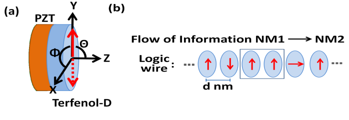
Each NM that we consider is a synthetic multiferroic stack with two layers - a magnetostrictive (Terfenol-D) and a piezoelectric (PZT) layer (Fig. 1a). Each layer is shaped like an elliptical cylinder. In the absence of any strain, the two (mutually anti-parallel) orientations along the major axis (the so-called ‘easy axis’) of the ellipse ( and = or in Fig. 1a) are stable magnetization orientations (degenerate potential energy minima of the magnet) that encode the binary bits ‘0’ and ‘1’ [11]. They are separated in energy by the shape anisotropy energy barrier [due to the anisotropic (elliptical) shape of the magnet] which prevents thermally-activated random and spontaneous switching between the two states. The barrier height is minimum when the magnetization vector lies in the plane of the magnet. We will call that the in-plane shape anisotropy barrier. Strain depresses this barrier and causes switching of the magnetization from one stable state to the other via an internally generated torque [12].
In this paper, instead of simulating logic bit propagation down a chain of sequentially clocked NM-s acting as a a binary wire, we will focus on the simplest dipole-coupled system of just two multiferroic nanomagnets NM1 and NM2, and study unidirectional information transmission from NM1 acting as input to NM2 acting as output (Fig. 1b). As long as the dipole coupling between the two magnets is not too strong, their magnetizations will be mutually anti-parallel in the ground state and hence the system will act as a simple inverter or NOT gate since the input and output bits are logic complements. If we flip the input magnetization, we will expect the output to flip in response, but this may not happen since the magnetization in NM2 may not be able to overcome the in-plane shape anisotropy barrier to switch (because the dipole interaction energy is much smaller than the shape anisotropy barrier). In other words, the system may remain stuck in a metastable state (NM1 and NM2 parallel) instead of reaching the ground state (NM1 and NM2 anti-parallel). To break the logjam, NM2 is mechanically stressed to depress the shape anisotropy barrier, and when the stress is withdrawn, it should flip to assume the anti-parallel configuration owing to dipole interaction. This strategy is known as Bennett clocking [13] which successfully transmits bit information unidirectionally from NM1 to NM2. In a long chain of many magnets, information is propagated unidirectionally from left to right by sequentially stressing the magnets to the right of the input magnet pairwise to rotate their magnetizations by large angles [14, 15].
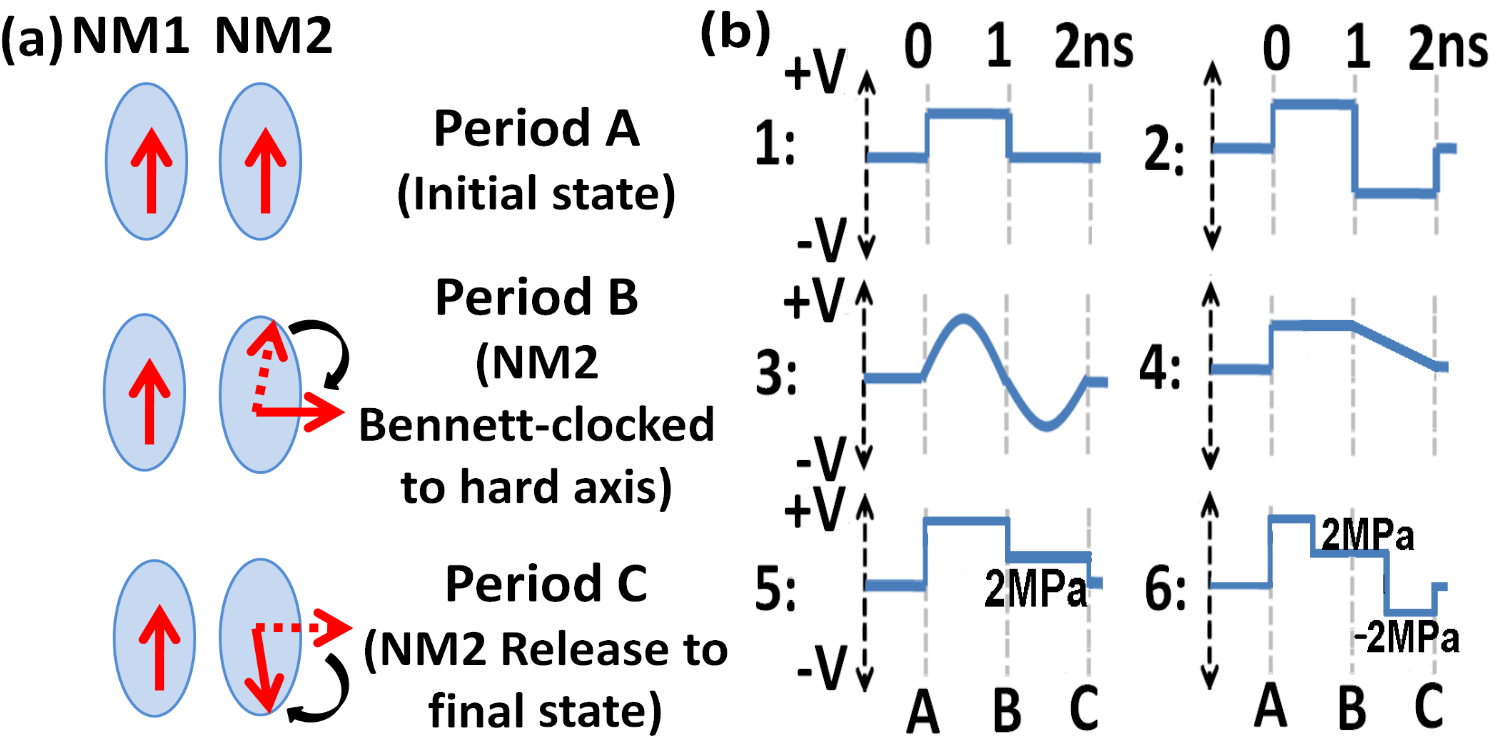
Fig. 2a shows the 3-step information transmission process in the inverter. In step A, information has just been written in NM1 (by flipping its magnetization with an external agent). In step B, NM2 is stressed (Bennett clocked) causing its magnetization to rotate. In step C, the stress on NM2 is withdrawn whereupon its magnetization should relax to the easy axis with the final orientation anti-parallel to that of NM1 because of dipole coupling [16]. If this fails to happen, an error is incurred. For the sake of completeness, we should also consider the case when the input to NM1 is such that it does not flip. Since the Bennett clocking is performed irrespective of the input state, the stress cycle in this case must not flip NM2; any flipping will result in an error. We do not discuss this case here since it is less error-prone than the other case. We will explore the switching profiles outlined in Fig. 2b, and study their switching reliability and delay. We note that the strain in the PZT responds to the applied voltage in timescales 100 ps [17]. Since our voltage pulse widths are 1 ns or more, we can neglect effects associated with finite rise and fall times of the stress in response to an abrupt voltage pulse.
Returning to the first case, successful switching of NM2 when NM1 is flipped is aided by two factors: (i) we need a high stress in step B to kick the magnetization of NM2 out of the initial orientation ( = or ) which are called stagnation points since the net torque on the magnetization due to stress vanishes at these precise locations, and (ii) we also need strong dipolar coupling between the two magnets in steps B and C when the magnetization of NM2 is near the in-plane hard axis ( and = 0 or ) so that the final orientation of NM2 upon stress release is anti-parallel to that of NM1. The stressing profile (stress versus time) for NM2 has to be designed with the above two facts in mind to minimize the switching error.
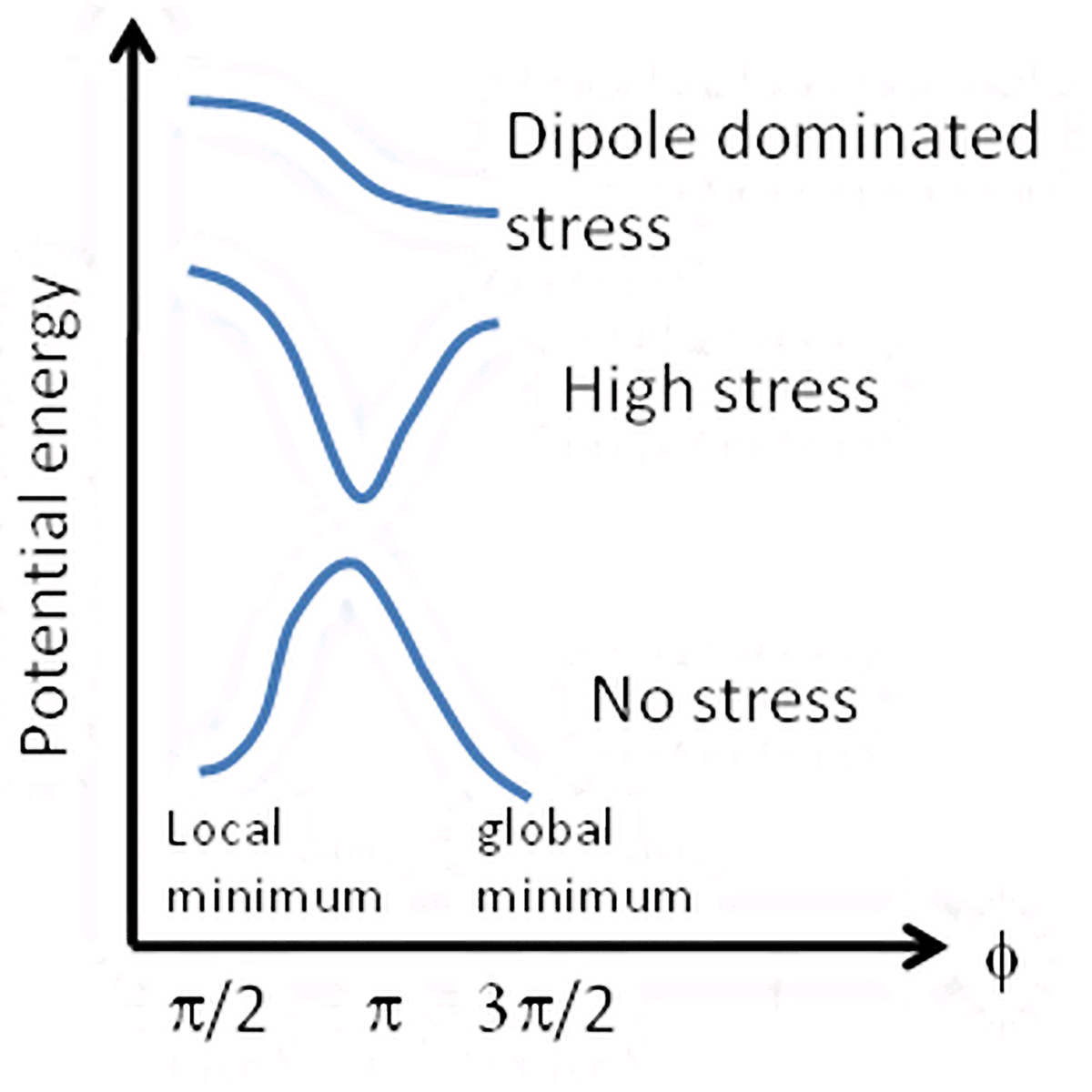
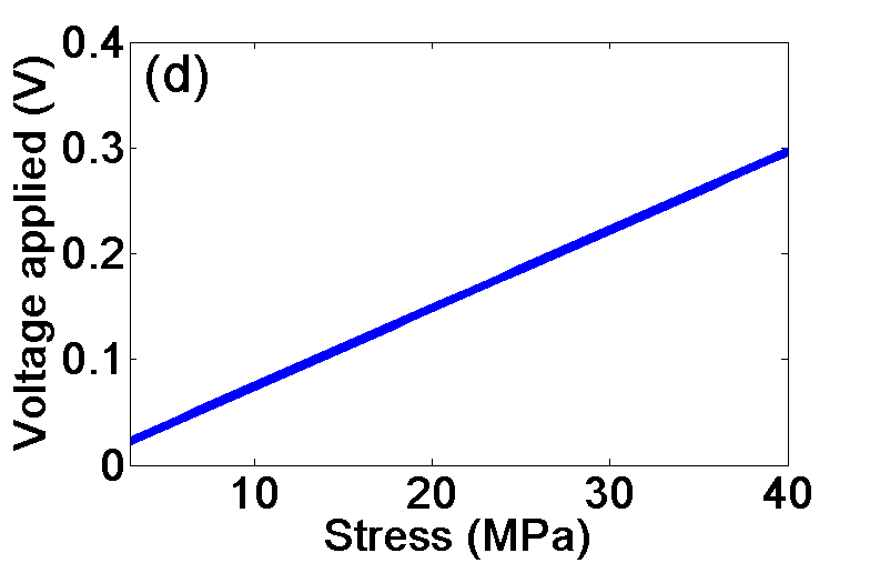
The minimum stress needed to kick the magnetization of NM2 out of a stable state along the easy axis is the critical stress. It is roughly that value of stress where the stress anisotropy energy offsets the in-plane shape anisotropy energy barrier. There is a range of stresses just above the critical stress where the stress anisotropy energy not only offsets the in-plane shape anisotropy energy barrier in NM2 but ensures that the only asymmetry in the potential energy landscape is due to the dipole coupling with NM1 (see upper curve of Fig. 2c). We call this the “dipole dominated region”. The asymmetry will reliably switch NM2 from (“up” in Fig. 2a) to (“down” in Fig. 2a) because there is only one energy minimum and it is located at . At higher stresses, the minimum energy location moves to (see the middle curve of Fig. 2c) and the magnetization will align along the minor axis of the elliptical magnet. When stress is finally withdrawn, the location will become the energy maximum and there will be a global minimum at (ground state) but there is also a local one at (metastable state) as shown in the bottom curve of Fig. 2c. Dipole interaction will make the global minimum lower in energy than the local minimum. Consequently, the magnetization will have some preference for the ground state () over the metastable state (), but thermal perturbations can take the system to the (wrong) metastable state. If it ends up there, then the in-plane shape anisotropy energy barrier will prevent it from reaching the global minimum, thus causing an error. Therefore, operating in the dipole dominated region reduces error rate but increases switching delay (because the stress is relatively weak), while operating at stress levels much above the dipole dominated region has the opposite effect. Fig. 2d shows the voltage needed to generate a certain amount of stress in the Terfenol-D NM, assuming complete strain transfer from the PZT to the Terfenol-D. The voltage was estimated by taking the PZT layer thickness to be 40 nm, Young’s modulus of Terfenol-D to be 30 GPa, and the d31 coefficient of PZT to be 1.8x10⁻¹⁰ m/V. All stress quantities in later figures can be converted to corresponding voltage quantities using Fig. 2d.
II Energy landscape of two dipole coupled nanomagnets (NM1 and NM2) and their magnetization dynamics
We will assume that NM2 has major axis a = 105 nm, minor axis b = 95 nm and thickness t = 6 nm, to ensure a 32 in-plane shape anisotropy energy barrier at room temperature. The numerical results in this paper depend on this value. Any combination of a, b and t that gives a barrier height of 32 will yield similar results. In choosing NM2’s dimensions, we only have to ensure that it always contains a single domain and therefore can be described by macrospin dynamics [18].
The temporal evolution of the magnetization in any single-domain NM, under the influence of an effective magnetic field , is described by the Landau-Lifshitz (LL) equation [19],
| (1) |
where is the Gilbert damping constant, is the gyromagnetic ratio and is the saturation magnetization. The quantity is the effective magnetic field acting on the magnetization due to shape anisotropy, strain and dipole interaction. It is the gradient of the magnet’s total potential energy with respect to the magnetization vector:
| (2) |
where is the vacuum permeability and is the magnet’s volume.
The potential energy of an NM is given by
| (3) |
where is the shape anisotropy energy due to the elliptical shape of the NM, is the stress anisotropy energy caused by the stress and is the dipoledipole interaction energy between the NMs. We ignore any magnetocrystalline anisotropy energy since the magnets are assumed to be amorphous. The shape anisotropy energy of the NM in spherical coordinates, and , is
| (4) |
where , and are respectively the demagnetization factors along the x-, y- and z-directions and are dependent on , and . The equations to calculate the demagnetization factors can be found in [20, 21]. The stress anisotropy energy in the element due to a stress applied along its major axis is
| (5) |
where is the is the saturation magnetostriction and is the applied stress. The quantity is negative for compression and positive for tension[21]. The dipole-dipole interaction energy between the -th and -th NMs is
| (6) |
where is the separation between their centers. For this study, we take d to be 150nm. We have assumed that the magnetostriction [22] and saturation magnetization [23]. The Gilbert damping constant for Terfenol-D is [24].
In the macrospin limit, the NMs were assumed to have uniform magnetization. To show that the macrospin limit is a good approximation, the switching dynamics were compared with detailed 3D micromagnetic simulations. Two micromagnetic packages were used: The Object Oriented MicroMagnetic Framework (OOMMF)[25] and M3[26]. Details of the comparison is in Appendix I.
The critical stress is the amount of stress needed to dislodge an NM’s magnetization from a stable orientation along the easy axis. This quantity depends on the in-plane shape anisotropy energy barrier and the magnetization orientation of its neighbors that determine the dipole interaction energy. The critical stresses required to rotate the magnetization of NM2 in isolation (no neighbors), in the configuration with NM1, and in the configuration with NM1 are, respectively:
| (7) |
| (8) |
| (9) |
These quantities are 3.14MPa, 2.72MPa and 3.56MPa, respectively, for = 150 nm.
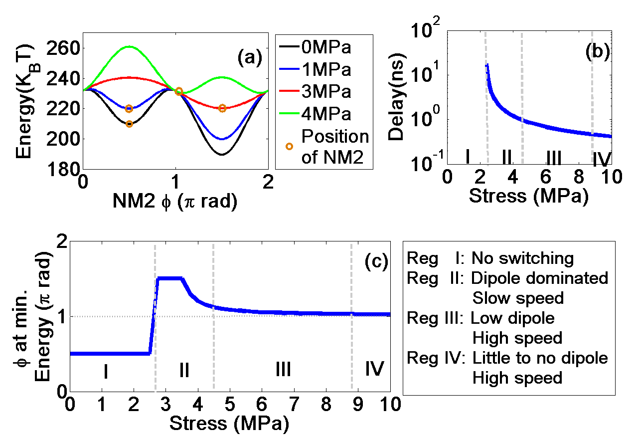
Fig. 3a shows the energy landscape and the stable (minimum energy) location of the magnetization vector of NM2 at different stress levels. At sub-critical stresses, the initial orientation of the magnetization () remains a local energy minimum so that the magnetization is trapped there and does not rotate. Close to the critical stress level of 3 MPa, the applied stress begins to cancel out the in-plane shape anisotropy energy barrier and the dipole interaction with NM1 dominates the energy landscape (we referred to this as the dipole-dominated regime). The energy minimum therefore moves to since dipole interaction favors anti-ferromagnetic ordering. As a result, the magnetization will rotate to the desired location (i.e. flip as desired), but because the stress is weak, rotation is slow and takes around 50 ns (Fig. 3b). At higher stress levels, the energy minimum shifts to the in-plane hard axis () since the stress anisotropy energy becomes overwhelmingly dominant. The high stress level speeds up the rotation. In Fig. 3c, we define three regions based on the location of the energy minimum. In Region I, for sub-critical stresses, the energy minimum is at and the magnetization does not switch at all. For the dipole dominated regime between 2.75 and 4.5 MPa (Region II), the minimum energy is close to so that the magnetization ultimately flips, albeit slowly since the stress is weak. In Regions III and IV, the stress starts to dominate the energy landscape and the minimum energy location is at . These different regions are associated with different switching error probabilities.
III Information transmission between two NMs taking thermal perturbations into account
Fig. 4a shows the room-temperature distribution of the azimuthal angle of the magnetization vector in NM2 during step A when it is in parallel configuration with NM1 at a distance of 150 nm. The thermal perturbations on the magnetization vector of NM2 are modeled by a Langevin random field that can be added to the effective magnetic field term in the LL equation. This field is related to the temperature by,
| (10) |
where is a white noise whose three components in Cartesian coordinates are Gaussians with zero mean and unit standard deviation [27]. The quantity is inversely proportional to the attempt frequency of thermal noise to flip magnetization and is the simulation time-step used to solve the coupled Landau-Lifshitz-Gilbert equation (describing the coupled dynamics of NM1 and NM2) numerically [28]. The peak of the distribution is at the stagnation point where for any applied stress.
IV Switching reliability
In this section, we study switching error probability as a function of pulse shape of the Bennett clock (stress versus time profiles) at room temperature. We also discuss trade off between error resilience and switching speed.
IV-A Case 1: abrupt stress application and removal
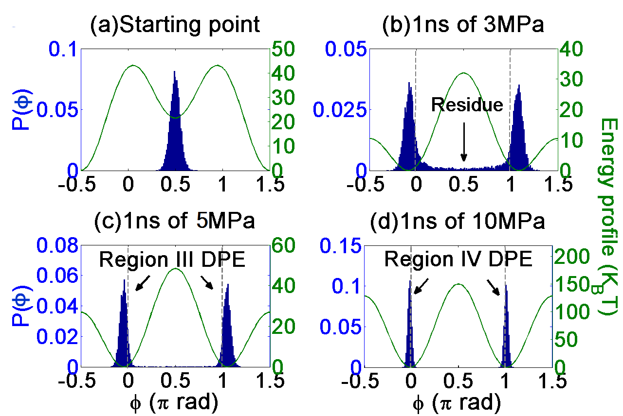
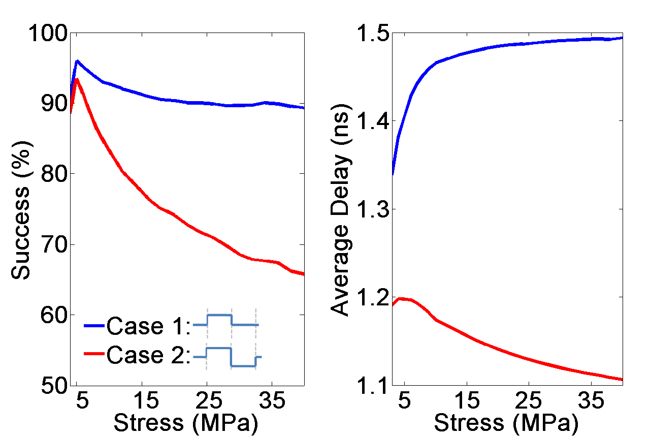
We consider the situation when the stress profile is a rectangular pulse turned on and off abruptly with infinite ramp rate (see case 1 in Fig. 2b). The pulse has a fixed width of 1 ns (legend of Fig. 5). Clearly, a pulse amplitude of 3 MPa is not sufficient to kick the magnetization vector out of the stagnation point with absolute certainty at the end of step B because of the appreciable residue around the starting orientation in the probability distribution of the magnetization (Fig 4b). This residue results in a low success rate. At a higher stress amplitude of 5 MPa (Fig. 4c, region III), the magnetization vector is kicked out of the starting orientation with high probability (near vanished residue). This stress is still low enough to allow dipole interaction to flip NM2 and steer the system to the anti-parallel configuration () with relatively high certainty. If we operate in this stress regime, then we will obtain a high success rate for switching to the correct anti-parallel configuration. If now the stress is further increased (region IV, Fig 4d), the influence of dipole interaction is diminished and the distributions become more symmetric about the hard axis. This means that upon releasing the stress, the 2-NM system has only slightly higher chances of going to the ground state (anti-parallel configuration and successful switching) than the metastable state (parallel configuration and switching failure). This explains why the success rate has a non-monotonic stress dependence and begins to decrease with increasing stress beyond an optimum stress (Fig. 5).
The highest success rate achieved with a 1 ns wide rectangular pulse is 95.97% at room temperature. It is achieved when the stress is 5 MPa. The thermally averaged switching delay at this stress is 1.38 ns. The last quantity is calculated by averaging over the delays associated with the successful switching trajectories among 10,000 trajectories whose starting points are chosen from the distributions of the initial magnetization orientation. The switching trajectories are computed by solving the stochastic LL equation (Equation (1) where is replaced with ).
IV-B Case 2: abrupt stress application, reversal and removal
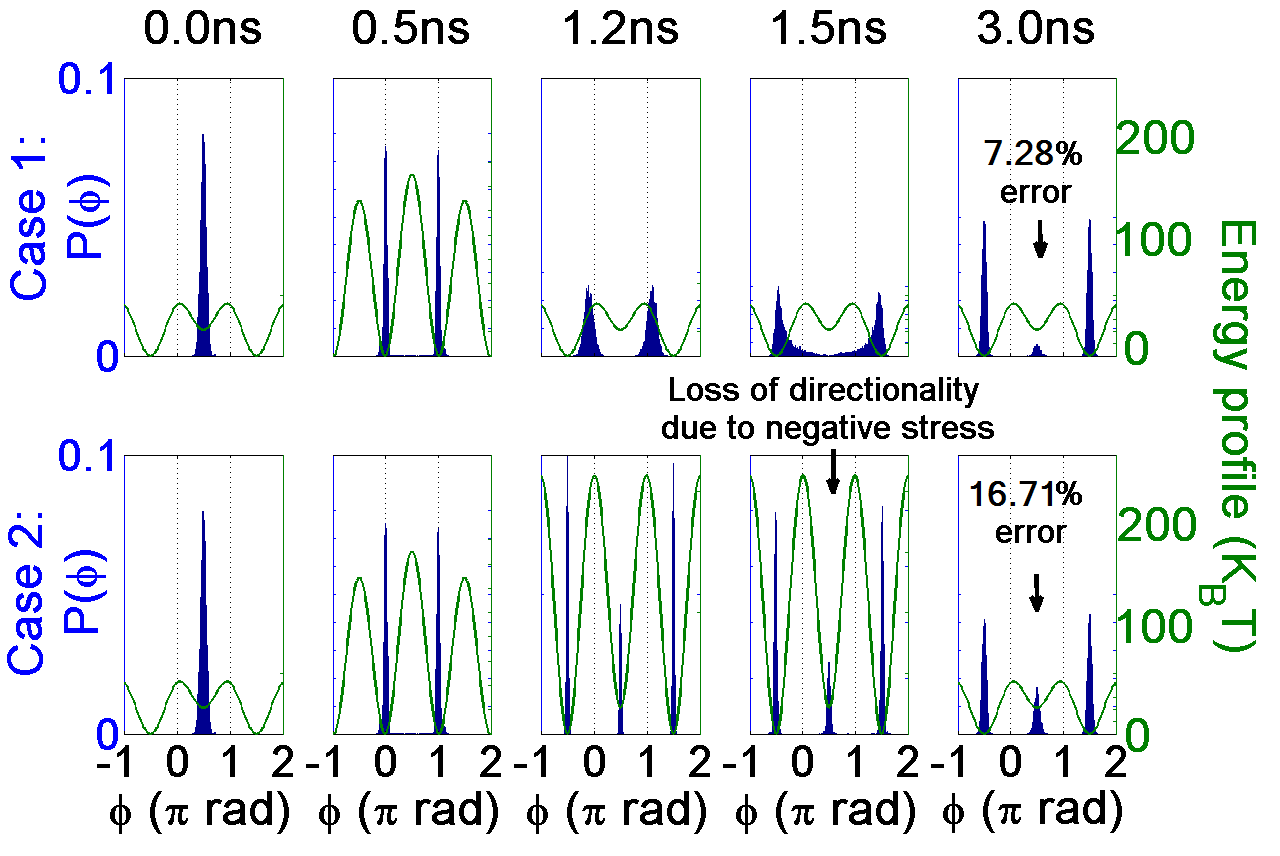
In order to switch faster, we can reverse the stress after 1 ns, so that a negative stress is applied during step C (legend of Fig.5). As expected, the success probability still peaks at the optimum stress of 5 MPa, but this probability is smaller than in Case 1. The success probability at high stresses also drops off much faster with increasing stress compared to Case 1. All this happens because negative stress actually raises the energy barrier between the two stable orientations along the easy axis instead of lowering this barrier. Therefore, in step C, the difference caused by dipole interaction between the energies of the two stable states of NM2 becomes a smaller fraction of the barrier height. As a result, the preference for the ground state of the inverter over the metastable state decreases. We call this loss of ‘dipole directionality’ since the dipole-induced preference for the anti-parallel ordering is eroded, resulting in a higher error rate. The average switching delay at the optimum stress however decreases and is now 1.2 ns. Case 2 therefore results in faster switching but a higher error rate compared to Case 1.
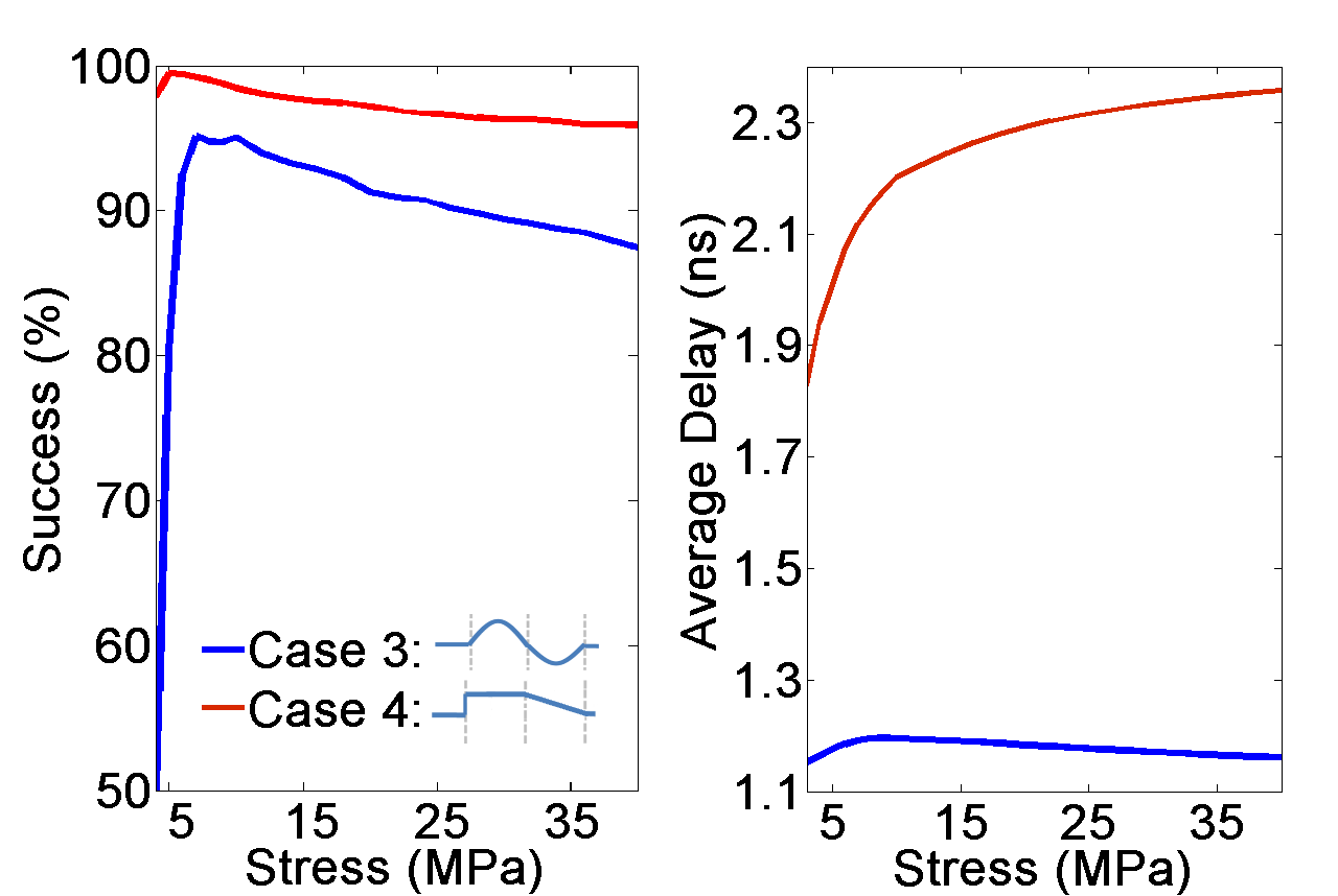
IV-C Cases 3 and 4: sinusoidal stress and tapered stress removal
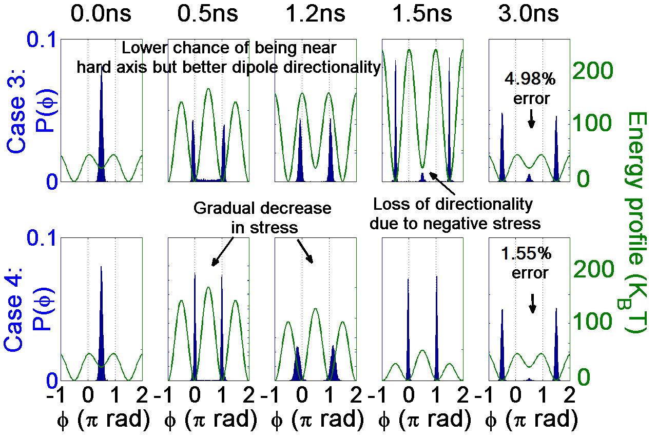
Case 3 pertains to a sinusoidal stress profile with a period of 2 ns (Fig. 7). Stress reversal during the negative cycle of the sinusoid switches the magnetization of NM2 faster, but the overall success rate is low as the sinusoidal stress during step B is not strong enough to kick the magnetization out of the stagnation point with high probability (Fig. 7). Furthermore, the negative stress during step C diminishes the role of dipole coupling as in Case 2. The thermally averaged switching delay at the stress level where success probability peaks is 1.2 ns (Fig.7).
Case 4 pertains to a linear ramp for stress withdrawal that we term tapered stress removal. After keeping the stress on for 1 ns, it is gradually removed in 1 ns instead of abruptly (with a constant ramp rate), achieving higher reliability than Cases 1, 2, and 3. The slow removal of stress allows the magnetization switching to operate in the dipole dominated stress region for a longer amount of time (Fig. 8). The thermally averaged switching delay is 2.02 ns at the stress level where the success probability peaks (Fig.7). For both cases 3 and 4, the success probability decreases with increasing stress beyond the optimum stress value because we end up spending less time in regions II and III as stress is increased.
IV-D Switching efficiently using region II - the dipole dominated regime
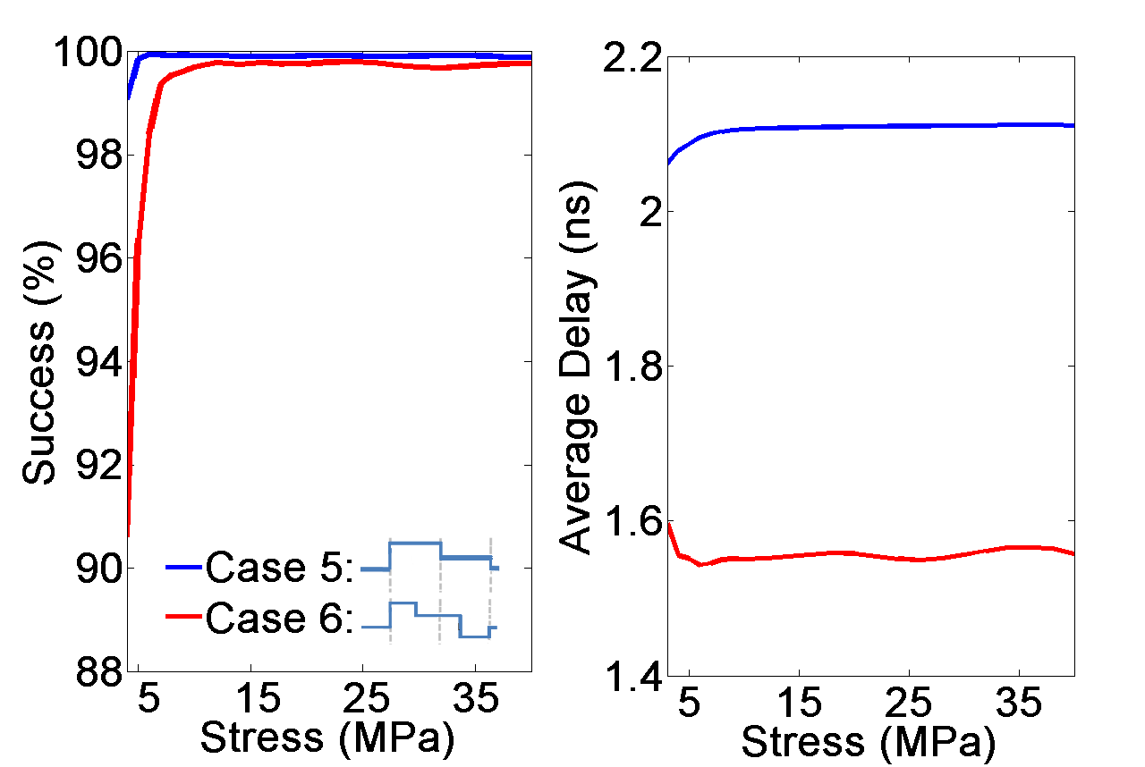
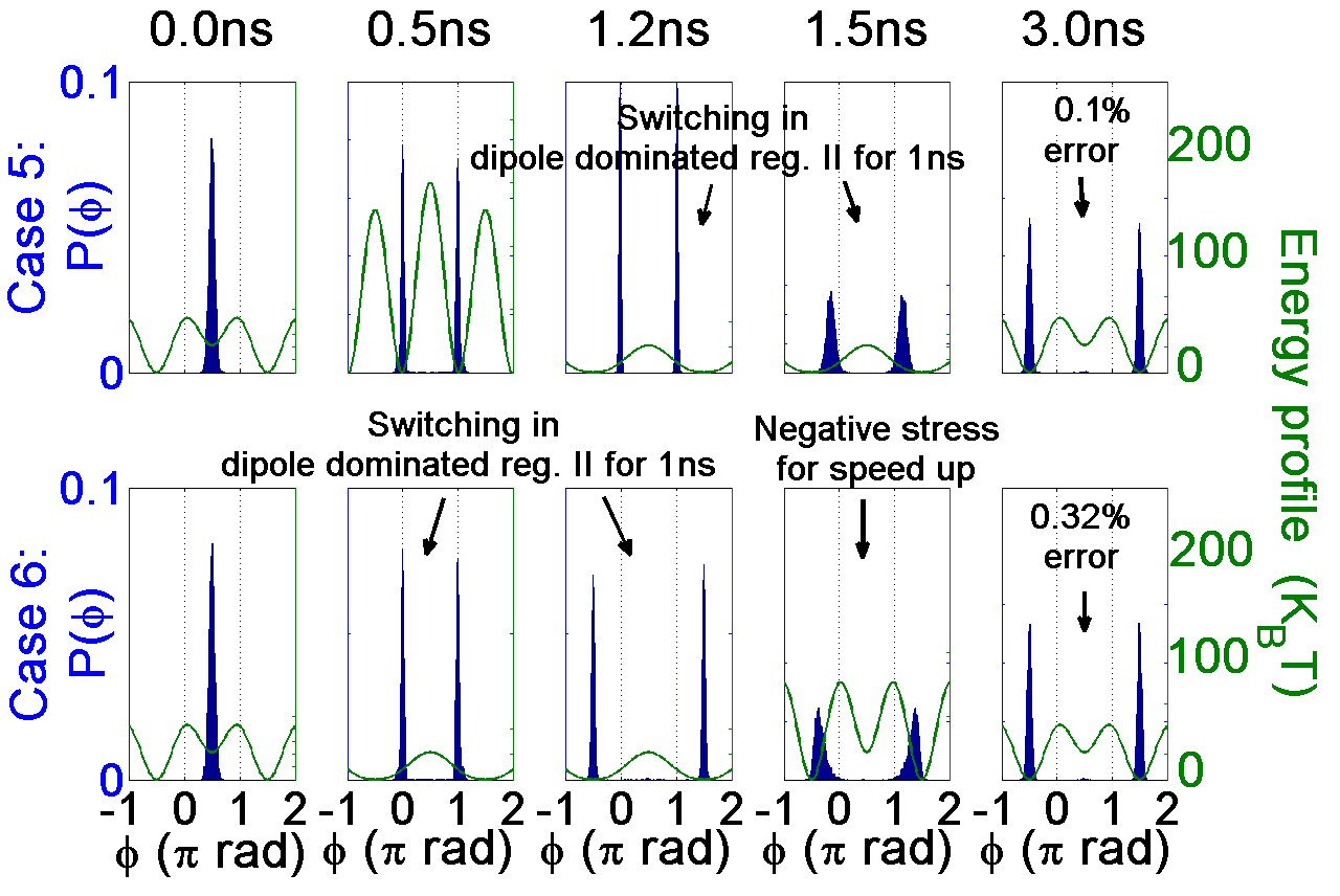
Cases 5 and 6 pertain to complex stressing profiles or pulse shapes shown in the legend of Fig. 9. Initially, in Case 5, a high stress is applied abruptly to NM2 to kick the magnetization out of the stagnation point. Then the stress is reduced abruptly to 3 MPA for 1 ns and finally withdrawn abruptly. During the last 1 ns (Fig. 10), the switch operates in region II where the dipole interaction dominated energy landscape nudges the magnetization to the correct final orientation to complete switching successfully. The success probability is much higher (99.9% for an initial stress of 10 MPa with a thermally averaged delay of 1.8 ns at room temperature).
In Case 6, a high stress is turned on abruptly, held for 0.5 ns, then reduced abruptly to 3 MPa, held for 1 ns, reversed abruptly to -3 MPa, held for 0.5 ns, and finally withdrawn abruptly. The stress reversal, as always, accomplishes faster switching (thermally averaged delay of 1.33ns) but at the cost of a slightly lower success probability of 99.68% for 10 MPa initial stress at room temperature.
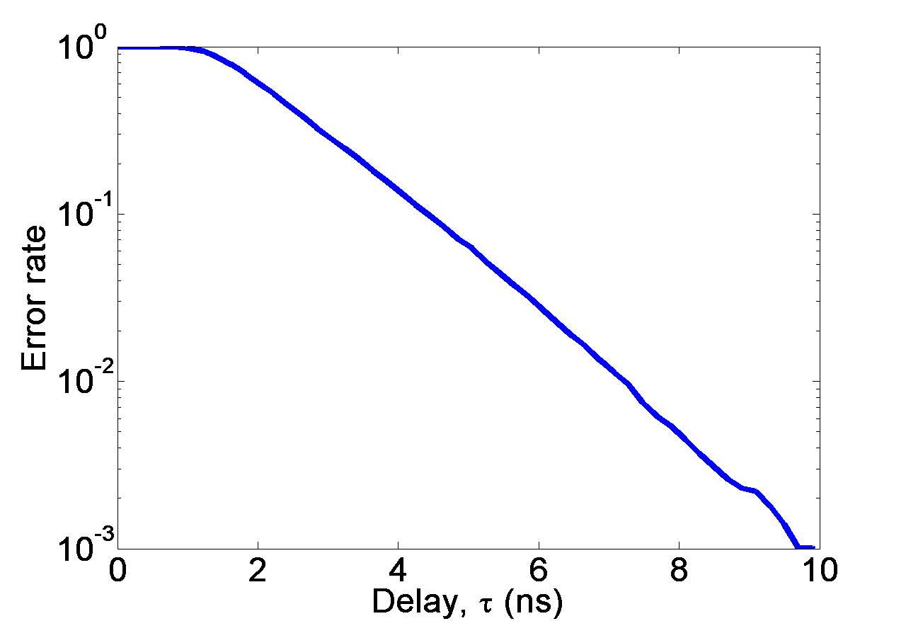
Unfortunately, even the best case scenario (case 5) with a room temperature success probability of 99.92% may not be good enough for contemporary logic which has stringent requirements on switching error probability. If we modify the stressing profile of Case 5 by continuing to stress NM2 at 2MPa beyond the 1 ns duration, a much lower error rate can be achieved (Fig. 11). However, this low error rate comes at the expense of a very long switching delay of 10 ns for an error probability of 10-3. Note that in this range, the error probability falls off nearly exponentially with increasing delay. If this trend could be extrapolated to much longer delays, then we could reach an error probability of at delays of 30 ns, provide the out-of-plane magnetization effects do not begin to dominate first. That error rate may be tolerable.
Another strategy to reduce error rate (without any pulse shaping) is to increase the shape anisotropy energy barrier of the magnets (make the ellipses more eccentric) which will allow us to increase the dipole coupling strength without inducing ferromagnetic ordering. The increased dipole coupling reduces error probability, but the stress needed to switch the magnets by overcoming the shape anisotropy energy barrier is now also larger, resulting in increased energy dissipation. Since SML is attractive for its low energy, it is imperative to keep the dissipation as small as possible, which is why we have not explored this case. Nevertheless, it should be kept in mind that there are two ways to reduce error probability: (1) by increasing switching delay (which we have discussed), or (2) by increasing energy dissipation (which we have alluded to but not discussed in detail). In the end, there is always a trade off between error probability and energy-delay product; better error-resilience can be purchased with higher energy-delay product.
| Case | Stress where | Peak success | Average switching |
|---|---|---|---|
| success rate | probability (%) | delay at peak(ns) | |
| peaks (MPa) | |||
| 1 | 5 | 95.97 | 1.38 |
| 2 | 5 | 93.45 | 1.21 |
| 3 | 7 | 95.12 | 1.13 |
| 4 | 5 | 99.49 | 2.02 |
| 5 | 6 | 99.92 | 1.82 |
| 6 | 12 | 99.77 | 1.33 |
V Conclusion
In this work, we used physical insights gained from the energy profiles of stressed magnets to devise various stressing profiles to reduce error rates in SML. Error rates small enough for logic may be achieved, but at very long switching delays. Thus, one disadvantage of dipole-coupled NML seems to be that it is very slow (clock speed should be few tens of MHz for reliable operation with acceptable error probabilities for logic at room temperature), but the energy advantage of SML still makes it an attractive paradigm for niche applications where speed is not the main concern, but energy-efficiency is. The application most suitable for SML-type technology is in medically implanted devices that need to harvest energy from the patient’s body movements without requiring a battery to operate. This has been discussed in ref. [4]
Acknowledgments
K. Munira and Y. Xie would like to thank Claudia K.A. Mewes and Andrew Tuggle from University of Alabama for useful discussion regarding M3. All authors acknowledge support from the US National Science Foundation under NEB 2020 grant ECCS-1124714 and the Semiconductor Research Corporation (SRC) under NRI Task 2203.001. J. A. and S. B also received support from the National Science Foundation under the SHF-Small grant CCF-1216614. J.A acknowledges support from NSF CAREER grant CCF-1253370.
Appendix I
To study the candidacy of various stressing profile for NML, the NMs were assumed to have uniform magnetization and their switching dynamics were studied with macrospin approximation. To show that the NMs can be treated as single domain magnets, their switching dynamics were compared with detailed three dimensional micromagnetic simulations. Two micromagnetic packages were used: The Object Oriented MicroMagnetic Framework(OOMMF)[25] developed in National Institute of Standards and Technology (NIST) and M3[26] in University of Alabama. In the micromagnetic simulation, the NM is divided into small cells and the magnetization in each cell is assumed to be uniform. The dimension of the NM is . The cell size is . Time integration of Landau-Lifshitz-Gilbert(LLG) equation is performed on each cell with effective field coming from exchange coupling, shape anisotropy and external magnetic field. To simulate Terfenol-D nano-magnet, the following parameters were used: saturation magnetization , exchange stiffness [29], and Gilbert damping factor . No magnetocrystalline anisotropy was taken into consideration.
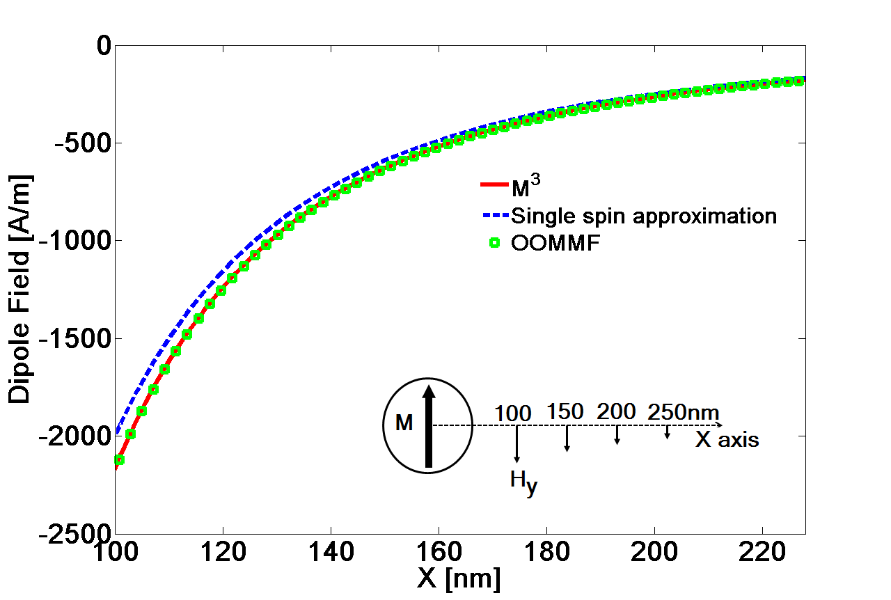
As information transfer from one NM to another takes place because of dipole coupling in NML, it is important to compare the dipole field of a multi domain system with single spin dipole approximation we use in our study where the magnet is assumed to be a single point (Eq. 6). The micromagnetic calculation is started with uniform magnetization across the NM and then relaxed it to its equilibrium configuration. Simulation is terminated when the residual torque satisfies . Fig. A1 shows the dipole field along the minor axis of the NM (). At , the field from the OOMMF simulation is about larger than the single spin dipole approximation. At this distance, the gradient of the field is also small, so inhomegeneity of the dipole field over the second magnet’s surface is not significant.
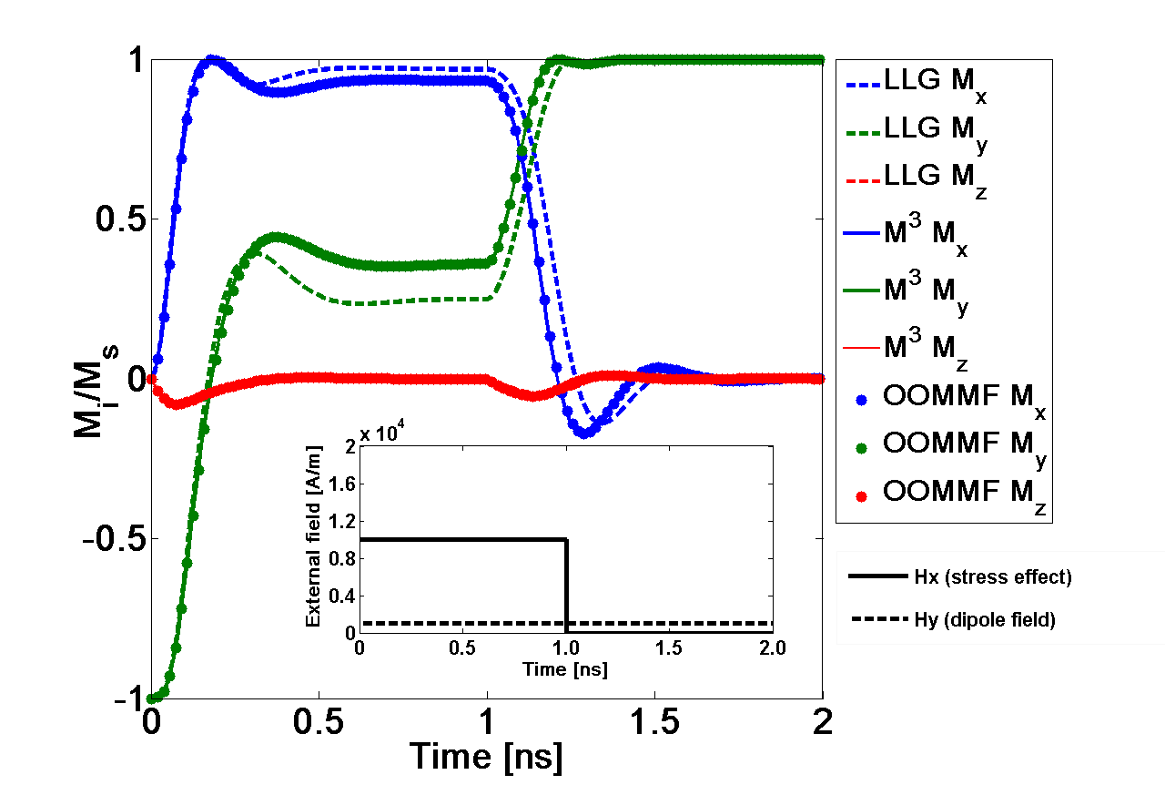
Since OOMMF/M3 cannot incorporate the effect of stress easily, a magnetic field is used to induce switching and the results are compared with macrospin calculation. A steady field of 1042 is applied along direction to simulate the dipole field from the adjacent magnet (calculated from a magnet with the same dimension at 120 nm distance). A sufficiently large magnetic field of 10 is then applied in the direction for 1 ns to simulate the stress. The magnetization of the adjacent magnet is assumed to be not affected by the switching of the magnet under study so its dipole field stays unchanged throughout the switching. Fig A1 shows the profile of external field and shows the comparison between micromagnetic simulation (OOMMF and M3) and single domain macrospin LLG simulation. The overall switching behavior is similar between the micromagnetic and LLG simulations. The slope of the switching curves are in close agreement which implies same switching speed. For all three simulations, the magnetization aligns with the Y axis after about 1.2ns. The discrepancy in the intermediate stage might come from some degree of non-coherency captured by micromagnetic simulation or a small discrepancy in the dipole field as indicated in the previous paragraph.
In conclusion, we have shown that single domain macrospin assumption in our study for NML is a reasonable approximation.
References
- [1] S. Bandyopadhyay and M. Cahay, “Electron spin for classical information processing: a brief survey of spin based logic devices, gates and circuits,” Nanotechnology, vol. 20, p. 412001, 2009.
- [2] A. Imre, G. Csaba, L. Ji, A. Orlov, G. H. Bernstein, and W. Porod, “Majority logic gate for magnetic quantum-dot cellular automata,” Science, vol. 311, no. 5758, pp. 205–208, 2006.
- [3] R. P. Cowburn and M. E. Welland, “Room temperature magnetic quantum cellular automata,” Science, vol. 287, no. 5457, pp. 1466–1468, 2000.
- [4] K. Roy, S. Bandyopadhyay, and J. Atulasimha, “Hybrid spintronics and straintronics: A magnetic technology for ultra low energy computing and signal processing,” Applied Physics Letters, vol. 99, no. 6, p. 063108, 2011.
- [5] “ITRS Report CORE9GPLL_HCMOS9_TEC_4.0 databook, STMicro,” 2003.
- [6] K. Roy, S. Bandyopadhyay, and J. Atulasimha, “Energy dissipation and switching delay in stress-induced switching of multiferroic nanomagnets in the presence of thermal fluctuations,” Journal of Applied Physics, vol. 12, p. 023914, 2012.
- [7] F. M. Spedalieri, A. P. Jacob, D. E. Nikonov, and V. P. Roychowdhury, “Performance of magnetic quantum cellular automata and limitations due to thermal noise,” IEEE Transactions on Nanotechnology, vol. 10, p. 537, 2011.
- [8] M. Fashami, K. Munira, S. Bandyopadhyay, A. Ghosh, and J. Atulasimha, “Switching of dipole coupled multiferroic nanomagnets in the presence of thermal noise: Reliability of nanomagnetic logic,” Nanotechnology, IEEE Transactions on, vol. 12, no. 6, pp. 1206–1212, Nov 2013.
- [9] M. S. Fashami, J. Atulasimha, and S. Bandyopadhyay, “Energy dissipation and error probability in fault-tolerant binary switching,” Sci. Rep., vol. 3, pp. –, Nov. 2013. [Online]. Available: http://dx.doi.org/10.1038/srep03204
- [10] K. Roy, “Critical analysis and remedy of switching failures in straintronic logic using bennett clocking in the presence of thermal fluctuations,” Applied Physics Letters, vol. 104, p. 013103, 2014.
- [11] K. Roy, S. Bandyopadhyay, and J. Atulasimha, “Switching dynamics of a magnetostrictive single-domain nanomagnet subjected to stress,” Phys. Rev. B, vol. 83, p. 224412, Jun 2011.
- [12] K. Roy, J. Atulasimha, and S. Bandyopadhyay, “Binary switching in a symmetric potential landscape,” SCIENTIFIC REPORTS, no. 3:3038, 2013.
- [13] C. H. Bennett, “The thermodynamics of computation - a review,” International Journal of Theoretical Physics, vol. 21, pp. 905–940, 1982.
- [14] J. Atulasimha and S. Bandyopadhyay, “Bennett clocking of nanomagnetic logic using multiferroic single-domain nanomagnets,” Applied Physics Letters, vol. 97, no. 17, p. 173105, 2010.
- [15] N. D’Souza, J. Atulasimha, and S. Bandyopadhyay, “Energy-efficient bennett clocking scheme for four-state multiferroic logic,” IEEE Transactions on Nanotechnology, vol. 11, pp. 418–425, 2012.
- [16] M. S. Fashami, K. Roy, J. Atulasimha, and S. Bandyopadhyay, “Magnetization dynamics, Bennett clocking and associated energy dissipation in multiferroic logic,” Nanotechnology, vol. 22, no. 15, p. 155201, 2011.
- [17] P. K. Larsen, G. L. M. Kampschoer, M. Van Der Mark, and M. Klee, “Ultrafast polarization switching of lead zirconate titanate thin films,” in Applications of Ferroelectrics, 1992. ISAF ’92., Proceedings of the Eighth IEEE International Symposium on, Aug 1992, pp. 217–224.
- [18] R. P. Cowburn, D. K. Koltsov, A. O. Adeyeye, M. E. Welland, and D. M. Tricker, “Single-domain circular nanomagnets,” Phys. Rev. Lett., vol. 83, pp. 1042–1045, Aug 1999.
- [19] G. Bertotti, C. Serpico, and I. Mayergoyz, Nonlinear Magnetization Dynamics in Nanosystems, Elsevier, Ed. Elsevier Science, 2008.
- [20] S. Chikazumi, Physics of Magnetism, Wiley, Ed. Wiley, 1694.
- [21] M. S. Fashami, J. Atulasimha, and S. Bandyopadhyay, “Magnetization dynamics, throughput and energy dissipation in a universal multiferroic nanomagnetic logic gate with fan-in and fan-out,” Nanotechnology, vol. 23, no. 10, p. 105201, 2012.
- [22] R. Abbundi and A. Clark, “Anomalous thermal expansion and magnetostriction of single crystal Tb.27Dy.73Fe2,” IEEE Transactions on Magnetics, vol. 13, no. 5, pp. 1519 – 1520, sep 1977.
- [23] K. Ried, M. Schnell, F. Schatz, M. Hirscher, B. Ludescher, W. Sigle, and H. Kronmüller, “Crystallization behaviour and magnetic properties of magnetostrictive TbDyFe films,” physica status solidi (a), vol. 167, no. 1, pp. 195–208, 1998.
- [24] J. Walowski, M. D. Kaufmann, B. Lenk, C. Hamann, J. McCord, and M. Manzenberg, “Intrinsic and non-local gilbert damping in polycrystalline nickel studied by Ti : sapphire laser fs spectroscopy,” Journal of Physics D: Applied Physics, vol. 41, no. 16, p. 164016, 2008.
- [25] M. J. Donahue and D. G. Porter, “OOMMF User’s Guide,” US Department of Commerce, Technology Administration, National Institute of Standards and Technology, 1999.
- [26] C. Mewes and T. Mewes. Matlab Based Micromagnetics Code M3. [Online]. Available: http://bama.ua.edu/ tmewes/Mcube/Mcube.shtml
- [27] J. Sun, “Spin angular momentum transfer in current-perpendicular nanomagnetic junctions,” IBM J. RES. & DEV., vol. 50, no. 1, pp. 81–100, 2006.
- [28] G. Brown, M. A. Novotny, and P. K. Rikvold, “Langevin simulation of thermally activated magnetization reversal in nanoscale pillars,” Physical Review B, vol. 64, p. 134422, 2001.
- [29] G. Dewar, “Effect of the large magnetostriction of terfenol-d on microwave transmission,” Journal of Applied Physics, vol. 81, no. 8, pp. 5713–5715, Apr 1997.