Stopping electrons with radio-frequency pulses in the quantum Hall regime
Abstract
Most functionalities of modern electronic circuits rely on the possibility to modify the path followed by the electrons using, e.g. field effect transistors. Here we discuss the interplay between the modification of this path and the quantum dynamics of the electronic flow. Specifically, we study the propagation of charge pulses through the edge states of a two-dimensional electron gas in the quantum Hall regime. By sending radio-frequency (RF) excitations on a top gate capacitively coupled to the electron gas, we manipulate these edge state dynamically. We find that a fast RF change of the gate voltage can stop the propagation of the charge pulse inside the sample. This effect is intimately linked to the vanishing velocity of bulk states in the quantum Hall regime and the peculiar connection between momentum and transverse confinement of Landau levels. Our findings suggest new possibilities for stopping, releasing and switching the trajectory of charge pulses in quantum Hall systems.
Electronic states in the quantum Hall regime — obtained for instance by applying a strong magnetic field to a two-dimensional heterostructure — are very peculiar; with a vanishing velocity in the bulk of the system, they only propagate (in a chiral way) on the edges of the sample. Following its initial discovery some thirty years ago Klitzing et al. (1980), the quantum Hall effect is now used for the metrological measurements of the quantum of conductance Hartland et al. (1991); Janssen et al. (2013) as well as a model system for mesoscopic physics, e.g. electronic interferometers Ji et al. (2003); Roulleau et al. (2008); Haack et al. (2011). The corresponding transport properties can be understood quantitatively in a very simple and elegant way using the Landauer-Büttiker scattering theory and the associated concept of one-dimensional chiral edge states Büttiker (1988). These edge states can take place on the actual edges of the sample — the mesa of the two dimensional electron gas — or can be defined by electrostatic gates put on top of the device. The field effect obtained by applying voltages on these gates is in turn very peculiar, not only does it allow one to close or open conducting paths (as in conventional field effect transistors) but it also modifies the actual paths taken by the electrons or even partitions the edge states into the superposition of two paths Ji et al. (2003); Roulleau et al. (2008).
Progress in RF quantum transport are made at an increasing rate Zhong et al. (2008); Dubois et al. (2013) so that single electron sources have now moved from theory to the lab Fève et al. (2007); Dubois et al. (2013). These newly available charge sources open a wealth of new possibilities for quantum electronics. In this letter, we discuss the dynamical manipulation of the path taken by the electron using fast RF modification of gate voltages. We send charge pulses from an Ohmic contact into the system. We find that these charge pulses can be dynamically manipulated by means of the gates voltages; they can be stopped, stored and their trajectories switched dynamically.
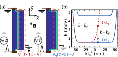
Mechanism for stopping single electron pulses. We start with defining our “stopping” protocol and the associated physical mechanism. Fig. 1(a,b) shows the first (simulated) sample that we consider. A two-dimensional electron gas (2DEG) under high magnetic field connected to two Ohmic contacts. We work in a regime where only the lowest Landau levels (LLL) contribute to the transport properties of the sample. It imposes that all variations of voltages are slow compared to the cyclotron frequency. The upper contact is grounded while the lower one is used to send voltage pulses through the system. A side gate, capacitively coupled to the right-hand side of the system (dashed line) allows one to modify the propagating edge states. When the gate voltage the current propagates through the middle of the sample [Fig. 1(a) left] while when the gate is grounded, the current propagates on the right edge of the sample [Fig. 1(a) right]. Fig. 1(a,b) are not simple schematics of the edge states but correspond to the extra electronic density that appears in the 2DEG upon imposing a DC bias voltage at the lower contact.
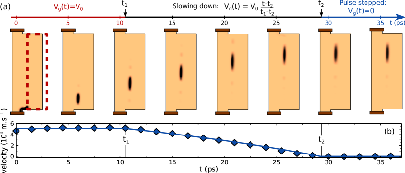
The upper part of Fig. 2(a) shows our “stopping” protocol. At time we send a voltage pulse through the lower contact in presence of a gate voltage [Fig. 1(a)]. We wait until the pulse has propagated up to (roughly) one third of the sample and at time we start decreasing the gate voltage . At time , and the gate is grounded [Fig. 1(b)]. The snapshots in Fig. 2(a) show that this protocol actually stops the propagation of the pulse which stays frozen in the system for .
The mechanism behind this behavior can be easily understood from an analysis of the eigenstates of the system. We model our system with the following Hamiltonian,
| (1) |
where , in the Landau gauge, is the magnetic field, is the effective mass of the system and the time-dependent potential contains contributions from the mesa boundary, the voltage pulse at the Ohmic contact and the electric field due to the side gate. In the absence of RF pulses, and assuming that our system is invariant by translation along the y-direction (which it is except close to the contacts but this is irrelevant), the LLL [that diagonalize Eq. (1)] are localized along the -direction and the plane waves along the -direction read,
| (2) |
where the magnetic length is defined by . In the absence of confining potential, the LLL are degenerate with an energy . Consequently they are dispersionless with vanishing velocity as . The presence of a confining potential breaks this degeneracy. Assuming (for the sake of the argument, our results stand without this assumption) that is smooth on the scale of , then the LLL remain eigenstates of the Hamiltonian in presence of the confining potential and their energy is simply raised by the value of at the center of the state, . The corresponding LLL are propagating on the edges. Fig. 1(b) shows the, numerically calculated, dispersion relations for (dashed red) and (blue).
Let us now go back to the “stopping” protocol. After we have sent the voltage pulse (), the system is in a superposition of LLL with energies close to the Fermi energy (we use ): . At , we start changing the gate voltage . Although now depends on time, we should bear in mind that the system remains invariant by translation along the -direction at all times. As a result the momentum is a good quantum number and the linear superposition of LLL is unmodified. The dispersion relation is now time-dependent with and the wave function reads, . In other words, the energy decreases at fixed momentum , as indicated by the arrow in Fig. 1(b). In particular the velocity of the pulse
| (3) |
decreases until it vanishes at where the pulse stops. This argument does not depend on the speed at which the gate voltage is varied as long as it is fast enough for the pulse not to escape the gated region before the velocity vanishes. The quantum Hall effect therefore gives us a way to modify the dispersion relation dynamically and trap particles in a region of vanishing velocity.
Numerical calculations. We perform direct numerical simulations of our RF protocol in order to check the above argument. Equation (1) is discretized on a lattice according to usual prescriptions Kazymyrenko and Waintal (2008) with standard parameters for heterostructures. We consider a 2DEG of density , corresponding to a Fermi energy or equivalently to a Fermi wave length . A magnetic field is applied to the system yielding a magnetic length and a cyclotron frequency (). We used a realistic confining potential for the gate that corresponds to a drift velocity but we did not actually solve the associated electrostatics. DC calculations are performed with Kwant Groth et al. (2014). RF simulations are performed with T-Kwant Gaury et al. (2014); Gaury and Waintal (2014).
In Fig. 2(a), a Gaussian pulse of duration and amplitude is sent through the system. Fig. 2(a) actually shows the difference between two simulations performed with and without the voltage pulse . Indeed, upon decreasing , the system relaxes to a new equilibrium (with electrons entering the system in order to fill the formerly forbidden region). We discuss this aspect briefly toward the end of this letter. As expected, we find that the pulse is indeed stopped for . More importantly, Fig. 2(b) shows a quantitative agreement between the numerics and the analysis made above. The symbols show the velocity of the pulse as measured from the time-dependent numerics (by looking at the time evolution of the center of mass of the electronic density carried by the pulse) while the line corresponds to Eq. (3).
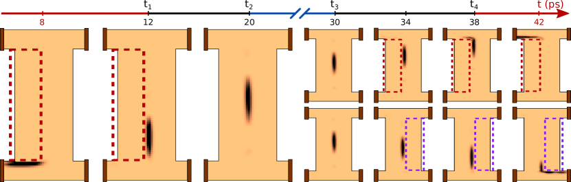
“Stop and release” protocol. Now that we have established the mechanism for stopping the pulse, we proceed with a slightly different sample with 4 terminals and an additional top gate, see Fig. 3. The first part of the protocol of Fig. 3 is the same as previously. We sent a pulse at (now the pulse is sent from the lower left contact and the left gate is polarized) and stop it by gradually grounding the left gate between and . For the voltage pulse is stuck in the middle of the sample. After waiting for some time, until , we do one of two things. Either we increase again the voltage of the left gate (upper panels) in order to restart the pulse, or we increase the voltage of the other (right) gate (lower panels) which also restarts the pulse but in a different direction. From a theoretical point of view, both cases are very similar and are essentially the counter-part of the stopping protocol (and can be analyzed accordingly). However, in practice they illustrate the versatility of what could be accomplished with this dynamical modification of the paths of the electrons. This RF protocol allows one to stop a charge pulse, then store it for a while in a region with vanishing velocity, and finally release it in a direction of our choice.
Probing “stopped and released” pulses with a Mach-Zehnder interferometer. We end this letter with a last set of simulations that allows
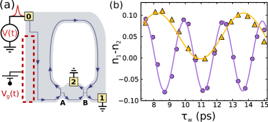
us to further analyze the nature of the “stop and release” protocol. In the sample sketched in Fig. 4(a), we send a voltage pulse, stop it with a gate (as previously), wait for some time , and release the pulse (again, as previously). However, instead of directly collecting the current in the electrode, it is sent through an electronic Mach-Zehnder interferometer obtained with two half-transmitting quantum point contacts A and B. We refer to Ji et al. (2003); Roulleau et al. (2008) (Kazymyrenko and Waintal (2008); Gaury and Waintal (2014)) for experimental (theoretical) details about the Mach-Zehnder geometry. Fig. 4(b) shows the difference between the total number of electrons collected at electrodes 1 () and 2 () as a function of the waiting time . The result is at first sight rather intriguing, oscillates with as . To understand this behavior, one needs to remember that a voltage pulse is not simply a localized charge pulse propagating in vacuum, indeed a delocalized plane wave (LLL) already exists before the pulse is sent. As one raises the bias voltage , the part of the wave at higher voltage starts accumulating an extra phase . Noting that (: number of injected particles) and supposing the voltage drop to be concentrated around , the wave function just after the pulse takes the form where is the Heaviside function. In other words a voltage pule generates a kink in the phase of the wave function. This kink, or phase domain wall, carries charges and propagates ballistically through the sample. The phase difference between the front and the rear of the pulse causes oscillations of with owing to the “dynamical control of interference pattern” Gaury and Waintal (2014). We now come back to our “stop and release” protocol (ignoring the presence of the voltage pulse). We suppose that the part of the edge state which is affected by the gate corresponds to (using curved coordinates that follow the edge state). Before , we have a plane wave . After , the inner part for oscillates as while the rest of the wave, unaffected by the gate, still oscillates as . Therefore, after the waiting time , a phase difference has been accumulated between the inner part and the outer one. When one releases the pulse again at time , the wave function reads . In other words, the “stop and release” procedure is equivalent to introducing two voltage pulses in series separated by a distance , one effective pulse of electrons followed by a counter-pulse of electrons. The oscillation shown in Fig. 4(b) simply follows from the “dynamical control of interference pattern” of Gaury and Waintal (2014) applied to this series of two pulses.
Qualitative discussion of charge relaxation in the system. Let us briefly discuss what happens in the “stopping” protocol when one does not send any voltage pulse in the system. We suppose, for the sake of the argument, that the gate is grounded very abruptly (). Just after the former edge state is frozen as discussed extensively above. On the other hand, a new one (which was at very high energy before ) now appears on the edge of the mesa. This edge state is initially empty and gets gradually filled as electrons pour in from the electrode. In our non-interacting model, only the propagating modes get filled in, leaving an empty puddle in the region of the 2DEG where the velocity vanishes (most of the area under the gate). This is of course unphysical as it raises the electrostatic energy of the system. As the new edge state is filled, the corresponding charges create a local electric field; the neighboring edge states become dispersive, and start to get filled as well. This process continues until all the LLL below the gate are filled and the system has relaxed to its equilibrium. This relaxation process should be very slow as the whole area underneath the gate needs to be filled while the electrons can only be poured in through one-dimensional edge states. A proper treatment of this physics would require solving the Poisson equation self-consistently with quantum mechanics. It would allow one to describe the charge relaxation using the compressible and incompressible regions discussed in Chklovskii et al. (1992). We expect however that the (current carrying) compressible stripes behave essentially in the same way as the edge states of the non-interacting theory used in this letter. Simulations of these phenomena will be the subject of future work. In any case, performing the difference between two simulations (with and without charge pulse) allows us to disentangle the pulse physics (of interest here) from the charge relaxation (poorly described by our model). A similar protocol should be followed experimentally.
Conclusion. RF quantum electronics is a very young emerging field. Here, we have presented a few possibilities offered in the quantum Hall regime. Even in the simplest situation, one predicts intriguing, often counter intuitive, results Gaury and Waintal (2014). We note that the practical implementation of the proposals presented in this letter imply delicate experiments where one injects high frequency pulses in a dilution fridge setup. The measurement scheme however should not be too difficult as, by periodically repeating the pulse sequences, measuring the number of electrons received in one electrode amounts to measuring DC currents.
Acknowledements. This work is funded by the ERC consolidator grant MesoQMC. We thank C. Bauerle, C. Glattli, L. Glazmann, F. Portier and P. Roche for useful discussions.
References
- Klitzing et al. (1980) K. v. Klitzing, G. Dorda, and M. Pepper, Phys. Rev. Lett. 45, 494 (1980).
- Hartland et al. (1991) A. Hartland, K. Jones, J. M. Williams, B. L. Gallagher, and T. Galloway, Phys. Rev. Lett. 66, 969 (1991).
- Janssen et al. (2013) T. J. B. M. Janssen, A. Tzalenchuk, S. Lara-Avila, S. Kubatkin, and V. I. Fal’ko, Reports on Progress in Physics 76, 104501 (2013).
- Ji et al. (2003) Y. Ji, Y. Chung, D. Sprinzak, M. Heiblum, D. Mahalu, and H. Shtrikman, Nature 442, 415 (2003).
- Roulleau et al. (2008) P. Roulleau, F. Portier, P. Roche, A. Cavanna, G. Faini, U. Gennser, and D. Mailly, Phys. Rev. Lett. 100, 126802 (2008).
- Haack et al. (2011) G. Haack, M. Moskalets, J. Splettstoesser, and M. Büttiker, Phys. Rev. B 84, 081303 (2011).
- Büttiker (1988) M. Büttiker, Phys. Rev. B 38, 9375 (1988).
- Zhong et al. (2008) Z. Zhong, N. Gabor, J. Sharping, A. Gaetal, and P. McEuen, Nature Nanotechnology 3, 201 (2008).
- Dubois et al. (2013) J. Dubois, T. Jullien, F. Portier, P. Roche, A. Cavanna, Y. Jin, W. Wegscheider, P. Roulleau, and D. C. Glattli, Nature 502, 659 (2013).
- Fève et al. (2007) G. Fève, A. Mahé, J.-M. Berroir, T. Kontos, B. Plaçais, D. C. Glattli, A. Cavanna, B. Etienne, and Y. Jin, Science 316, 1169 (2007).
- Kazymyrenko and Waintal (2008) K. Kazymyrenko and X. Waintal, Phys. Rev. B 77, 115119 (2008).
- Groth et al. (2014) C. W. Groth, M. Wimmer, A. R. Akhmerov, and X. Waintal, ArXiv1309.2926, to appear in New J. Phys. (2014).
- Gaury et al. (2014) B. Gaury, J. Weston, M. Santin, M. Houzet, C. Groth, and X. Waintal, Physics Reports 534, 1 (2014).
- Gaury and Waintal (2014) B. Gaury and X. Waintal, Nat. Commun. 5, 3844 (2014).
- Chklovskii et al. (1992) D. B. Chklovskii, B. I. Shklovskii, and L. I. Glazman, Phys. Rev. B 46, 4026 (1992).