Controllable Spin-Charge Transport in Strained Graphene Nanoribbon Devices
Abstract
We theoretically investigate the spin-charge transport in two-terminal device of graphene nanoribbons in the presence of an uniform uniaxial strain, spin-orbit coupling, exchange field and smooth staggered potential. We show that the direction of applied strain can efficiently tune strain-strength induced oscillation of band-gap of armchair graphene nanoribbon (AGNR). It is also found that electronic conductance in both AGNR and zigzag graphene nanoribbons (ZGNRs) oscillates with Rashba spin-orbit coupling akin to the Datta-Das field effect transistor. Two distinct strain response regimes of electronic conductance as function of spin-orbit couplings (SOC) magnitude are found. In the regime of small strain, conductance of ZGNR presents stronger strain dependence along the longitudinal direction of strain. Whereas for high values of strain shows larger effect for the transversal direction. Furthermore, the local density of states (LDOS) shows that depending on the smoothness of the staggered potential, the edge state of AGNR can either emerge or be suppressed. These emerging states can be determined experimentally by performing spatially scanning tunneling microscope or by scanning tunneling spectroscopy. Our findings open up new paradigms of manipulation and control of strained graphene based nanostructure for application on novel topological quantum devices.
pacs:
72.80.Vp,72.25.-b,73.43.-f,77.65.LyI Introduction
The atomically thick layer of carbon atoms with a honeycomb lattice structure - known as graphene - still keeps attracting considerable deal of attention due to its potential use in electronics. Graphene presents several exotic physical properties, such as the quantum spin Hall effect (QSHE) Kane and Mele (2005a, b), associated with a nontrivial topological time-reversal invariant state that has a bulk energy gap; and a pair of gapless spin filtered edge states at the sample boundaries. Recently, another striking topological phenomenon has attracted a notable interest, i.e. the quantum anomalous Hall effect (QAHE) Xiao, Chang, and Niu (2010). This topological phenomenon appears if one of the spin channels in the QSH state is suppressed by the own sample magnetization, with the emergence of an electronic topological phase transition, characterized by quantized Hall conductance in an insulating state. This interesting phenomena predicted to be host in graphene Qiao et al. (2012, 2010), has been experimentally observed in topologically magnetic thin films Chang et al. (2013), with a great promise in spintronic applications Hasan and Kane (2010).
A mechanism highly desirable in the development of spin-based devices is the effective control of the spin current flow Žutić, Fabian, and Das Sarma (2004). To obtain polarized electronic current, one of the essential strategies is the creation of an effective potential barrier for a given spin specie, while the other can flow with no resistance. Also, the energy gap control, is an important issue related to the on-off electrical tuning Xia et al. (2010). One of the key elements to implement graphene based nanostructure in spintronic devices, relies upon the role of spin-orbit coupling (SOC). In graphene, there are two different SOC contributions: (i) the extrinsic Rashba SOC, originated from the inversion symmetry breaking due to the substrate, which can also be manipulated by applied electric field Huertas-Hernando, Guinea, and Brataas (2006); López-Sancho and Muñoz (2011); Zarea and Sandler (2009) and (ii) the intrinsic SOC (ISO) arising from the carbon atomic SOC - which is known to give rise to the existence of spin-polarized edge states in the QSH phase Haldane (1988); Kane and Mele (2005a, b); Hasan and Kane (2010).
Mechanical deformations have a significant effect on the electronic, quantum transport and optical properties of a material and is used in the silicon electronics industry to boost device performance. For graphene and graphene nanoribbons (GNR) both experiments Mohiuddin et al. (2009); Ni et al. (2008); Huang et al. (2010); Levy et al. (2010); Yan et al. (2012) and simulations Pereira, Castro Neto, and Peres (2009); Gui, Li, and Zhong (2008); Pellegrino, Angilella, and Pucci (2010) have confirmed that the band structure can be dramatically altered by strain deformation. For instance, due to the breaking of sublattice symmetry, an uniaxial strain may induce a change of topology of the Fermi line, a merging of two inequivalent Dirac points and a tunable band gap at point Pereira, Castro Neto, and Peres (2009); Pellegrino, Angilella, and Pucci (2010). Thus, it may be used to trigger a quantum phase transition from a semi-metal to a semiconductor.
A combination of basic elements of uniaxial strain, SOC, exchange field, and staggered potential leads to a very exotic physics Diniz, Guassi, and Qu (2013). For instance, intrinsic SOC is favorable for opening a bulk energy gap around Dirac points Haldane (1988); Kane and Mele (2005a, b), while Rashba SOC depresses the gap Bercioux and De Martino (2010); Zarea and Sandler (2009). Then intrinsic and Rashba SOCs make an opposite contribution to the topological phase of QSHE. Besides, Rashba SOC breaks down inversion symmetry and exchange term breaks down time-reversal symmetry (TRS). Thus changing RSO and exchange interaction may lead to a QSH to QAH phase transition Qiao et al. (2012, 2010), which can be further manipulated by the application of uniaxial uniform strains Diniz, Guassi, and Qu (2013). Although, the quantum conductance of GNRs under uniaxial strain has been previously reported Topsakal and Ciraci (2010); Lu and Guo (2010); Wang, Liu, and Liu (2012), the spin related terms and staggered potential were not taken into account.
In this paper, we aim to analyse the electronic transport control and the LDOS in GNR with different terminations in the QAHE phase by means of uniform strain deformations and smoothness of staggered potential. The electronic transport can be performed by using a two-terminal device akin to a field electron transistor (FET). QAHE phase can be determined experimentally, by on-site spin-resolved density of states, that can be accessed by spatially scanning tunneling microscope (STM) or by scanning tunneling spectroscopy (STS) Morgenstern (2011); Stolyarova et al. (2007); Li et al. (2013).
II Theoretical Model
We consider GNR with homogeneous SOCs, exchange field interaction and staggered potential. The uniaxial strain is included through the introduction of strain-dependent hopping parameters. The Hamiltonian for this system in the real space reads
| (1) |
where is the nearest-neighbor -band tight-binding Hamiltonian. The fermionic operators / creates/anihilates an electron at site i with spin () and hopping amplitude . The unstrained eV Pereira, Castro Neto, and Peres (2009) and the deformed lattice distances are related to the relaxed ones by , where the uniaxial strain tensor is given in ref. Pereira, Castro Neto, and Peres (2009). For simplicity, we set the unstrained C-C distance to be unity. is the Rashba spin-orbit with interaction with parameter proportional to the electric field applied perpendicular to the - plane of the graphene Kane and Mele (2005b); Zarea and Sandler (2009); Huertas-Hernando, Guinea, and Brataas (2006), are the Pauli spin matrices. is the intrinsic SOC, and the vectors points from site to , which for the intrinsic SOC with coupling parameter , which connects the next nearest-neighbors through Haldane (1988); Kane and Mele (2005a, b). corresponds to the uniform exchange field with strength , responsible for breaking TRS of the system Tse et al. (2011) and refers to the staggered sublattice confining potential with , being for sublattice with value at the edges Li, Sheng, and Xing (2012). The is strongly dependent across the transversal direction, and decays exponentially from the edges with a characteristic width .
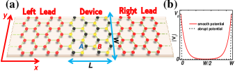
To calculate the spin-resolved conductance and the LDOS, we have implemented the standard surface Green’s function approach Nardelli (1999); Sancho, Sancho, and Rubio (1985, 1984). The GNR device is divided into three regions: left lead, central conductor and right lead, as schematically shown in Fig. 1 (a) for an AGNR. Notice that denotes the number of zigzag chains and to the number of dimer lines. The uniaxial strain is applied to either the longitudinal (=0) or the transversal (=), or at any arbitrary angle with respect to the -axis. The central conductor is the only region under the influence of SOC effects, exchange field and staggered potential; it is also connected to semi-infinite leads by nearest-neighbor hopping. To avoid surface mismatch Bahamon and Pereira (2013), we have considered that the leads are also strained. Therefore, a perfect atomic matching at the interface leads/central conductor is achieved. The Green’s function of the device (omitting the spin indices) is then calculated by
| (2) |
where denotes the advanced/retarded Green’s function, is the energy () of the injected electron (the Fermi energy at a given doping). stands for the Hamiltonian in the central region and are the self-energies that describe the influence of the left/right leads, , where is the Green’s function for the semi-infinite lead, obtained through an iterative procedure of the tight-binding Hamiltonian Nardelli (1999), and couples each lead to the central region. The spin resolved conductance through the system is given by,
| (3) |
where the trace runs through the lattice sites at the central conductor, is the quantum of conductance per spin, and are the couplings for the leads, related to the spin-diagonal self-energies by Nardelli (1999).
III Results
In what follows, we focus on a ZGNR () with a specific width of 5.4nm and length of 10.93nm (while in absence of strain). Similarly, we have chosen a metallic AGNR, i.e , with being a positive integer, with approximately same width and length. It is important to mention that wider the ribbon, more conducting channels can be available for higher doping, therefore the problem becomes more complex for both ZGNR and AGNR. Although, close to the Fermi level there will be the same amount of conducting channels for the pristine metallic nanoribbons. We have also checked the length dependence, and it is indeed relevant to the device prototype, as the scattering region, i.e. the region of the device has the effects of SOC, exchange field and staggered potential enhanced, as the injected electron can feel such fields in a longer length scale. Although we choose a specific length, the results presented here show a general behavior of such devices.
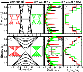
To illustrate the band structure of pristine GNR under uniaxial strains, we assume that except for the first term all other terms in Eq. 1 are set to zero. Fig. 2 (a) and (d), show the electronic structure of unstrained and strained (insets) ZGNR and AGNR with nearest-neighbors hopping, while (b) and (e) plot their correspondent density of states. In contrast, (c) and (f) illustrate the conductance profiles. One can notice the edge states of ZGNR (thick solid line) at the Fermi level for 26-ZGNR, is robust against uniaxial strains, as demonstrated in panel (b) and (c). The ribbon is metallic due to the strain-robust zero-energy flat band, and the conductance turns out to be an integer multiple of the quantum conductance , as the channels are completely transparent. For high energy doping, there is only a slightly change in the plateaus, and as the ZGNR has two distinct valleys, the conductance increases always by 4.
In strong contrast, the band structures of the AGNR families (semiconducting or metallic) are highly sensitive to the tensile uniaxial strain. As strain increases, the electrical conductivity may change from an insulator to a conductor or vice-versa. But, the prominent effect is observed near the Fermi level, as strain can induce a band gap in an otherwise metallic AGNRs, or change an existent band gap in semiconducting ribbons in a non-monotonic way Lu and Guo (2010). This band gap can be explained by the strain-induced shifting of the Dirac point, similar to previous works on deformed carbon nanotubes Yang and Han (2000). For instance, strains drastically change the electronic behavior of metallic 47-AGRN, shown in (d), responsible for an electronic topological transition (ETT) from metallic to semiconductor. It manifest itself for the appearance of a vanishing density of states close to the charge neutrality point (highlighted in the inset of panel (e)). In addition, the transport gap () shows a strain direction dependence, which has been intensively explored by other authors Lu and Guo (2010); Topsakal, Bagci, and Ciraci (2010); Rasuli, Rafii-Tabar, and zad (2010); Poetschke et al. (2010), which demonstrated that is robust even across strained junctions or intrinsic defects Bahamon and Pereira (2013); Lehmann, Ryndyk, and Cuniberti (2013).
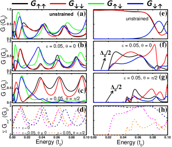
To study the conductance characteristics in presence of both Rashba SOC and exchange field, we set the parameters =0.1, =0.2, and =0. Notice that with these parameters, the system is in the QAHE phase Qiao et al. (2012). Nevertheless, if the ISO parameter is different from zero, there is an upper-limited value of Qiao et al. (2012); Diniz, Guassi, and Qu (2013), beyond which a new phase characterized by a vanishing Chern Number =0 can take place; this phase is the so-called TRS-broken QSH phase Yang et al. (2011); Qiao et al. (2012); Diniz, Guassi, and Qu (2013). The spin-resolved conductance is shown in Fig. 3: for (a) unstrained, (b) strained along , (c) strained along and (d) the total conductance of a ZGNR. Notice that there is a suppression for both the spin conserving and the spin-flip conductance components for either unstrained or strained ZGNR in the energy range considered. However, these backscattering (transmission dips) at certain precise energies at the first plateau are different depending on the strain configuration, and a close inspection shows that conducting channels for non-spin flip and spin-flip conductances oscillate. Depending on the Fermi energy and set parameters, certain conductance components can even be completely suppressed. This suppression is attributed to the appearance of quasi-localized states in the device, which may produce sharp scattering resonances, also known as resonant backscattering which is a general behavior of quasi-1D quantum systems Gómez-Medina et al. (2001). For higher energies, however, the large number of conducting channels leads to a non-vanishing transmission, as the channels get mixed along the device, and results in the appearance of an interchannel backscattering dominated by interference effects. Therefore, in the QSH phase protected by the TRS, nonmagnetic impurities do not cause backscattering on each boundary, and the spin transport in the edge states is dissipationless at zero temperature. In the QAH phase, however, there is a weak scattering between forward and backward movers, leading to a low-dissipation spin transport. At low energy, this interesting strain-controllable behavior of conducting channel suppression might be efficiently used to filter electrical current of desired spins, in spin filtering devices. In Fig. 3 (d), we show the total conductance, which is nearly robust against strains, specially close to the charge neutrality point, where the deviations due to strain are quite small. In contrast, the conductance of AGNR shows a drastic modification, with the development of a transport gap, which is insensitive to the electron spin that is injected-collected in the device. However, this induced transport gap is dependent upon the direction of the applied strain, with a larger conduction suppression along (red dashed line) with = 0.04 , and = 0.086 while along , that can be observed in panel (h). Also, the total conductance exhibits different plateaus: around and approximately in AGNR without and with strain, respectively, which is one less quantum of conductance available for the electron to be transmitted along the device.
Another remarkable phenomenon is the oscillatory dependence of the spin components of on the value of , which is shown in Fig. 4 (a)-(d), where the curves correspond to different topological GNRs and strain setups for . The same parameters are used as the Fig. 3, except for . To reveal the effects of Rashba SOC, we set =0 in the calculation. Then, the system is time-reversal invariant and the conductance components and . This oscillatory behavior is reminiscent of the spin field effect transistor (FET) and has a similar source Datta and Das (1990), as the spin precesses as it propagates in the presence of the Rashba field, acquiring a net phase that is proportional to , where is the length of the device. Further inspecting the strain-induced band gap in 47-AGNR in presence of SOC and exchange field interactions, one notices that in Fig. 4 (e) a similar band gap oscillation characteristic as reported in a earlier work Lu and Guo (2010). In the regime of small strain, the band gap shows approximately linear response, with increasing values of strain, however, it starts to oscillate. Further investigation shows that the amplitude and period of the gap-oscillation are tuned by direction of the strain, as shown in Fig. 4 (e). A specific dependence of transport-gap on the angle of the strain is clearly depicted in Fig. 4 (f). Notice that the transport gap is indeed strongly tuned by strain-direction. It equals approximately zero at 0.1, while it reaches 0.086 at 0.5.
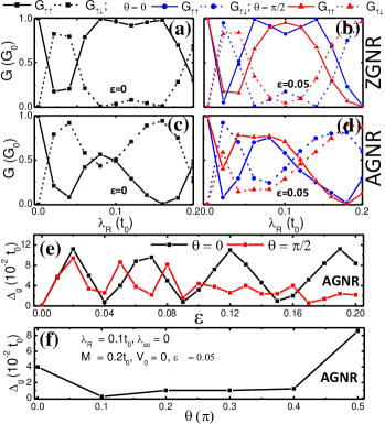
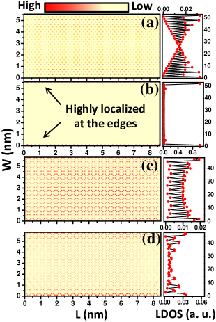
Fig. 5 (a)-(d) show the theoretical STM maps for an incoming electron with Fermi energy of =0.05 for =0.1, =0.05 and =. The panels on the right show the LDOS across the transversal direction. These STM maps can be experimentally accessible by performing a STM or through a STS measurements. The calculation has been performed by using the LDOS, , and with the aid of a -atomic orbital to smooth out the STM maps. It is important to mention that the system is in the QAHE, with a non-zero Chern number Qiao et al. (2012). Fig. 5 (a)-(b), show the highly localized edge states present in ZGNR in the QAHE phase. Breaking of the TRS due to the exchange field, leads to a suppression for the spin down states in (a). Nevertheless, for the spin up there is an emerging edge localization as shown in (b). In contrast, no edge localization is found in AGNR as shown in Fig. 5 (c)-(d). Therefore, the conductance in AGNR is achieved by the bulk conducting channels.
To further inspect the edge state behavior and its robustness against a smooth staggered sublattice potential, we have calculated the LDOS for different parameter configurations for both 26-ZGNR and 47-AGNR for fixed =0.05, with parameters =0.1, =0.05 and =. In Fig. 6 (a)-(f), we show the LDOS across at exactly the middle of the device, i.e. at a length , of the 26-ZGNR while (g)-(l) corresponds to 47-AGNR, for different set of parameters. For 26-ZGNR, we can notice that the LDOS is robust against strain with a slight modification on the amplitudes of the LDOS. However, when a staggered sublattice potential is considered by setting =6, smoothness parameter dependent behavior emerges. For instance, by setting =0.1 implies in the suppression of the LDOS in one of the edges for a given spin. Also, there is a clear asymmetry, that can be explained by the A/B sublattice asymmetry - in one side, the edge terminates in A-site, while in the other in B-site. This characteristic makes the staggered potential being an effective barrier - indeed for both spin species when =4.0 is set - as the staggered potential can be considered as a non-magnetic impurity. Also, the LDOS amplitudes has some important changes while applying strain with along longitudinal () and transversal direction (), which can be understood by compression/elongation of the ribbon width that is directly associated to the length smoothness of the staggered potential.
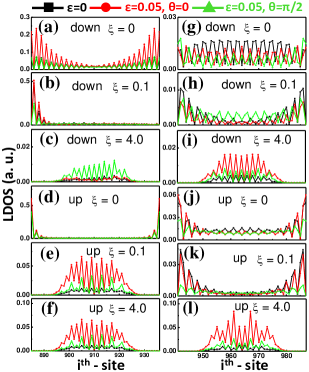
For the case of an AGNR, away from strain induced transport gap (in fact it does not change the strain induced transport gap), we can also observe changes in the LDOS amplitude for different strain configurations. However, some important aspects can be observed by adding a staggered potential: (i) - for , that would correspond to a less smooth potential (the potential effectively zero in the central region of the ribbon), there is an emerging localization in the AGNR akin to the edge states usually observed in ZGNR Li, Sheng, and Xing (2012), and perfectly symmetric on both edges as it does have same sublattice termination. (ii) for , that would correspond to smother staggered potential, the edge localized LDOS is fully suppressed for both spin species, and the contributing conducting channels are now at the central region. So the transition from an abrupt to a smoother staggered potential might be traced down to a topological phase transition with the quenching of an emerging edge state, therefore the Chern number is expected to vanish in this condition Qiao et al. (2012); Diniz, Guassi, and Qu (2013).
IV Conclusions
In summary, we have investigated the spin-resolved electronic transport and LDOS of GNR devices under the influence of SOC, exchange field, smooth staggered potential and uniform uniaxial strains. Our results demonstrate that it is possible to achieve a total electron transmission suppression of specific spin specie, which can be further tailored by uniaxial tensile strain on specific directions. Furthermore, by including a graded staggered potential, the following interesting behaviors have been observed in the LDOS maps: (i) selective edge conducting channel suppression for ZGNR for a sharper staggered potential and (ii) emerging of an edge state for AGNR for sharper staggered potential, which is associated to a topological phase transition Li, Sheng, and Xing (2012). These results suggest a possible implementation of a field-effect topological quantum transistor based on strained GNR, thus paving the way for the development of novel topological quantum devices.
Acknowledgements.
We thank discussions with M. Ezawa, Shu-Shen Li and Z. Qiao. We acknowledge financial support received from CAPES, FAP-DF and CNPq.References
- Kane and Mele (2005a) C. L. Kane and E. J. Mele, Phys. Rev. Lett. 95, 146802 (2005a).
- Kane and Mele (2005b) C. L. Kane and E. J. Mele, Phys. Rev. Lett. 95, 226801 (2005b).
- Xiao, Chang, and Niu (2010) D. Xiao, M.-C. Chang, and Q. Niu, Rev. Mod. Phys. 82, 1959 (2010).
- Qiao et al. (2012) Z. Qiao, H. Jiang, X. Li, Y. Yao, and Q. Niu, Phys. Rev. B 85, 115439 (2012).
- Qiao et al. (2010) Z. Qiao, S. A. Yang, W. Feng, W.-K. Tse, J. Ding, Y. Yao, J. Wang, and Q. Niu, Phys. Rev. B 82, 161414 (2010).
- Chang et al. (2013) C.-Z. Chang, J. Zhang, X. Feng, J. Shen, Z. Zhang, M. Guo, K. Li, Y. Ou, P. Wei, L.-L. Wang, Z.-Q. Ji, Y. Feng, S. Ji, X. Chen, J. Jia, X. Dai, Z. Fang, S.-C. Zhang, K. He, Y. Wang, L. Lu, X.-C. Ma, and Q.-K. Xue, Science 340, 167 (2013).
- Hasan and Kane (2010) M. Z. Hasan and C. L. Kane, Rev. Mod. Phys. 82, 3045 (2010).
- Žutić, Fabian, and Das Sarma (2004) I. Žutić, J. Fabian, and S. Das Sarma, Rev. Mod. Phys. 76, 323 (2004).
- Xia et al. (2010) F. Xia, D. B. Farmer, Y.-m. Lin, and P. Avouris, Nano Letters 10, 715 (2010).
- Huertas-Hernando, Guinea, and Brataas (2006) D. Huertas-Hernando, F. Guinea, and A. Brataas, Phys. Rev. B 74, 155426 (2006).
- López-Sancho and Muñoz (2011) M. P. López-Sancho and M. C. Muñoz, Phys. Rev. B 83, 075406 (2011).
- Zarea and Sandler (2009) M. Zarea and N. Sandler, Phys. Rev. B 79, 165442 (2009).
- Haldane (1988) F. D. M. Haldane, Phys. Rev. Lett. 61, 2015 (1988).
- Mohiuddin et al. (2009) T. M. G. Mohiuddin, A. Lombardo, R. R. Nair, A. Bonetti, G. Savini, R. Jalil, N. Bonini, D. M. Basko, C. Galiotis, N. Marzari, K. S. Novoselov, A. K. Geim, and A. C. Ferrari, Phys. Rev. B 79, 205433 (2009).
- Ni et al. (2008) Z. H. Ni, T. Yu, Y. H. Lu, Y. Y. Wang, Y. P. Feng, and Z. X. Shen, ACS Nano 2, 2301 (2008).
- Huang et al. (2010) M. Huang, H. Yan, T. F. Heinz, and J. Hone, Nano Letters 10, 4074 (2010).
- Levy et al. (2010) N. Levy, S. A. Burke, K. L. Meaker, M. Panlasigui, A. Zettl, F. Guinea, A. H. C. Neto, and M. F. Crommie, Science 329, 544 (2010).
- Yan et al. (2012) H. Yan, Y. Sun, L. He, J.-C. Nie, and M. H. W. Chan, Phys. Rev. B 85, 035422 (2012).
- Pereira, Castro Neto, and Peres (2009) V. M. Pereira, A. H. Castro Neto, and N. M. R. Peres, Phys. Rev. B 80, 045401 (2009).
- Gui, Li, and Zhong (2008) G. Gui, J. Li, and J. Zhong, Phys. Rev. B 78, 075435 (2008).
- Pellegrino, Angilella, and Pucci (2010) F. M. D. Pellegrino, G. G. N. Angilella, and R. Pucci, Phys. Rev. B 81, 035411 (2010).
- Diniz, Guassi, and Qu (2013) G. S. Diniz, M. R. Guassi, and F. Qu, Journal of Applied Physics 114, 243701 (2013).
- Bercioux and De Martino (2010) D. Bercioux and A. De Martino, Phys. Rev. B 81, 165410 (2010).
- Topsakal and Ciraci (2010) M. Topsakal and S. Ciraci, Phys. Rev. B 81, 024107 (2010).
- Lu and Guo (2010) Y. Lu and J. Guo, Nano Research 3, 189 (2010).
- Wang, Liu, and Liu (2012) J. Wang, Z. Liu, and Z. Liu, AIP Advances 2, 012103 (2012).
- Morgenstern (2011) M. Morgenstern, physica status solidi (b) 248, 2423 (2011).
- Stolyarova et al. (2007) E. Stolyarova, K. T. Rim, S. Ryu, J. Maultzsch, P. Kim, L. E. Brus, T. F. Heinz, M. S. Hybertsen, and G. W. Flynn, PNAS 104, 9209 (2007).
- Li et al. (2013) G. Li, A. Luican-Mayer, D. Abanin, L. Levitov, and E. Y. Andrei, Nat. Commun. 4, 1744 (2013).
- Tse et al. (2011) W.-K. Tse, Z. Qiao, Y. Yao, A. H. MacDonald, and Q. Niu, Phys. Rev. B 83, 155447 (2011).
- Li, Sheng, and Xing (2012) H. Li, L. Sheng, and D. Y. Xing, Phys. Rev. Lett. 108, 196806 (2012).
- Nardelli (1999) M. B. Nardelli, Phys. Rev. B 60, 7828 (1999).
- Sancho, Sancho, and Rubio (1985) M. P. L. Sancho, J. M. L. Sancho, and J. Rubio, Journal of Physics F: Metal Physics 15, 851 (1985).
- Sancho, Sancho, and Rubio (1984) M. P. L. Sancho, J. M. L. Sancho, and J. Rubio, Journal of Physics F: Metal Physics 14, 1205 (1984).
- Bahamon and Pereira (2013) D. A. Bahamon and V. M. Pereira, Phys. Rev. B 88, 195416 (2013).
- Yang and Han (2000) L. Yang and J. Han, Phys. Rev. Lett. 85, 154 (2000).
- Topsakal, Bagci, and Ciraci (2010) M. Topsakal, V. M. K. Bagci, and S. Ciraci, Phys. Rev. B 81, 205437 (2010).
- Rasuli, Rafii-Tabar, and zad (2010) R. Rasuli, H. Rafii-Tabar, and A. I. zad, Phys. Rev. B 81, 125409 (2010).
- Poetschke et al. (2010) M. Poetschke, C. G. Rocha, L. E. F. Foa Torres, S. Roche, and G. Cuniberti, Phys. Rev. B 81, 193404 (2010).
- Lehmann, Ryndyk, and Cuniberti (2013) T. Lehmann, D. A. Ryndyk, and G. Cuniberti, Phys. Rev. B 88, 125420 (2013).
- Yang et al. (2011) Y. Yang, Z. Xu, L. Sheng, B. Wang, D. Y. Xing, and D. N. Sheng, Phys. Rev. Lett. 107, 066602 (2011).
- Gómez-Medina et al. (2001) R. Gómez-Medina, P. San José, A. García-Martín, M. Lester, M. Nieto-Vesperinas, and J. J. Sáenz, Phys. Rev. Lett. 86, 4275 (2001).
- Datta and Das (1990) S. Datta and B. Das, Appl. Phys. Lett. 56, 665 (1990).