Electronic Raman Scattering On Individual Single Walled Carbon Nanotubes
Abstract
We report experimental measurements of electronic Raman scattering under resonant conditions by electrons in individual single-walled carbon nanotubes (SWNTs). The inelastic Raman scattering at low frequency range reveals a single particle excitation feature and the dispersion of electronic structure around the center of Brillouin zone of a semiconducting SWNT (14, 13) is extracted.
pacs:
81.07.De, 73.63.Fg, 73.22-fMany experimental techniques for the study of electronic properties surrender in intrinsic one-dimensional systems particularly single-walled carbon nanotubes (SWNTs) owing to their low dimension and richness of geometric structures. Typical examples include the magneto-electric transport technique and angle-resolved photoemission spectroscopy which informatively probe the band dispersion (around Fermi level with electric transport though) and electron’s quantum states in 3D and 2D materials, but lose ground in SWNTs. As yet, there lacks a method capable of directly evaluating the band dispersion in SWNTs. Resonant Raman spectroscopy has been recognized as one of the most powerful and popular characterizing technique in SWNT research. SWNTs’ geometric structure could be quantitatively identified at individual nanotube level with the well established protocols in resonant Raman spectroscopyM. S. Dresselhaus, G. Dresselhaus, R. Saito, and A. Jorio, Physics Reports 409, 47 (2005). Intensive efforts in Raman spectroscopy focus on the scattering by characteristic phonons as well as the modes of collective lattice vibrations. And the electronic aspects are implicitly addressed in Raman study through scattering intensity owing to various resonant conditions, energy shift due to electron-phonon couplingK.-i. Sasaki, R. Saito, G. Dresselhaus, M. S. Dresselhaus, H. Farhat, and J. Kong, Physical Review B 78, 235405 (2008)and spectrum lineshape in presence of Breit-Wigner-Fano (BWF) lineshape due to phonon-plasmon coupling and electron-electron interactionsM. S. Dresselhaus, G. Dresselhaus, R. Saito, and A. Jorio, Physics Reports 409, 47 (2005); M. S. Dresselhaus, G. Dresselhaus, A. Jorio, A. G. Souza Filho, and R. Saito, Carbon 40, 2043 (2002); E. H. Hasdeo, A. R. T. Nugraha, K. Sato, M. S. Dresselhaus, and R. Saito, Physical Review B 88, 115107 (2013).
Recently Farhat et al. reported a mode of electronic Raman scattering (ERS) from metallic SWNTs, where the Raman shift changes with the excitation energy and the energy of scattered photon is exactly resonant with the excitonic transition energyH. Farhat, S. Berciaud, M. Kalbac, R. Saito, T. Heinz, M. Dresselhaus, and J. Kong, Physical Review Letters 107 (2011). The electric-doping modulation on the ERS shows that this mode of ERS originates from the electron-hole excitation by Coulomb exchange at the linear band of metallic SWNTs. However, the other ERS modes, for example, the ones arising from single particle and collective elementary excitations which carry information on the energy and wave-vector dispersions have not been observed yet. There exist several obstacles toward the observation of ERS in SWNTs: (i) It is overwhelmed by the substrate scattering and lattice vibration scattering at finite temperature; (ii) The ERS originating from single particle and collective excitations is usually around a few in terms of energy, and therefore very close to the excitation laser. It is technically challenging to distinguish such low frequency Raman signal from Rayleigh scattering; (iii) Most resonant Raman scattering on individual SWNTs is collected with confocal-like micro-Raman setup to maximize the light collecting power, where the incident light and scattered light are both at normal direction with respect to the SWNT axis. The momentums of the incident and scattered photons are orthogonal to the electron momentum dispersion and therefore the photon and electron elementary excitations are decoupled at normal incidence due to 1D nature of SWNTs. Here we report the observation of electronic Raman scattering around from a small suspended SWNT bundle. We study the low frequency Raman spectra on SWNTs under the resonant excitation at oblique incident angles. The energy of the ERS shows linearly proportional to the momentum exchange with the interacting photons along the SWNT axis. We attribute the ERS to the single-particle excitation, and the energy-momentum dispersion of the resonant band could be directly evaluated.
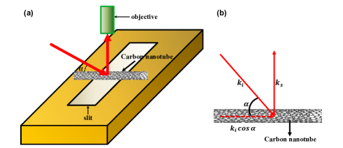
wide long slits on silicon substrates were fabricated with a standard microelectromechanical (MEMS) process, including low pressure chemical vapor deposition (LPCVD) silicon nitride etching mask growth, optical lithography, reactive ion etching (RIE) and wet etching. The SWNTs were in situ synthesized by chemical vapour deposition (CVD) across the slits. The catalyst was prepared by selectively dipping the diluted solution of on the silicon substrate and then by being reduced under 400 SCCM/50 SCCM at for . Individual SWNTs were grown on the substrates in ethanol vapor with the same gas mixture at for . The low frequency Raman signals were collected with a notch filter and a single stage monochromator(HR800, Jobin Yvon), which demonstrates much higher throughput than dual or triple stage monochromators, with high Rayleigh rejection rate at low frequency range. The ERS was observed with the resonant laser (HeNe, ) at oblique angels against the SWNT axis, as sketched in Figure 1. Rayleigh scattering spectroscopy was carried out with a supercontinuum photonic fiber in a similar way as ref H. Zeng, H. Zhao, F.-C. Zhang, and X. Cui, Physical Review Letters 102, 136406 (2009); M. Y. Sfeir, F. Wang, L. Huang, C.-C. Chuang, J. Hone, S. P. O’Brien, T. F. Heinz, and L. E. Brus, Science 306, 1540 (2004).
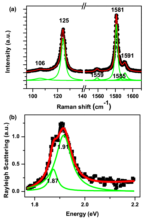
Characteristic resonant Raman spectra and Rayleigh scattering spectroscopy were used to identify the sample as shown in Figure 2. G-band Raman spectroscopy as shown in Figure 2(a) indicates that our sample is a small bundle of semiconducting SWNTs with frequency and linewidth , as well as at , and which can be tentatively used to estimate the diameter of the tubesA. Jorio, et al., Physical Review B 66, 115411 (2002); A. Jorio, et al., Physical Review B 65, 155412 (2002). From the linear relation of between nanotube diameters and the inverse of their Radial Breathing Mode (RBM) frequencies of suspended SWNTsK. Liu, W. Wang, M. Wu, F. Xiao, X. Hong, S. Aloni, X. Bai, E. Wang, and F. Wang, Physical Review B 83, 113404 (2011), we further obtained values of diameter of our SWNTs to be and . The interband transition was determined by Rayleigh scattering spectroscopy. As shown in Figure 2(b), Lorentzian fitting yields two peaks at and respectively. According to the atlas of carbon nanotubesK. Liu, et al., Nat Nano 7, 325 (2012)with effect of intertube coupling in bundles consideredF. Wang, et al., Physical review letters 96, 167401 (2006), our samples are assigned to consist of (14, 13) SWNT and (23, 9) SWNT with Rayleigh scattering peak positions redshifted by and respectively. Values of diameter of these two SWNTs calculated by ( is the nearest-neighbor C-C distance)K. Liu, W. Wang, M. Wu, F. Xiao, X. Hong, S. Aloni, X. Bai, E. Wang, and F. Wang, Physical Review B 83, 113404 (2011) are consistent with those given by RBM Raman spectroscopy (Figure 2(a)). The peak at in Rayleigh scattering spectrum shown in Figure 2(b) is from the third optical transition () of SWNT with chiral indices (14, 13), while the one at corresponds to of nanotube (23, 9).
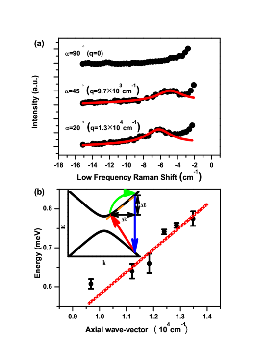
Figure 3 shows the representative low frequency Raman scattering from the SWNT under resonant excitations at oblique incident angles. A small bump (Figure 3(a)) gradually rises from none at normal incidence to a few wave number (around ) at oblique incidence. The bump shows blue-shifted with the decrease of incident angle. The corresponding energy has a linear dependence on , the projection of the incident photon wave-vector along the SWNT axis. To our knowledge, the lowest frequency of phonon mode at -point was in the range of Y.-K. Kwon, S. Saito, and D. Tománek, Physical Review B 58, R13314 (1998), bigger than our Raman results with frequency ranging from to . Besides, slope of acoustic phonon dispersion near -point can be estimated to be R. Saito, G. Dresselhaus, and M. S. Dresselhaus, Physical properties of carbon nanotubes (World Scientific, 1998), which is two orders of magnitude smaller than our results. Therefore, possible origins associated with phonon dispersion can be ruled out. The position of the small bump is independent of the excitation intensity in the range of . Thus the bump unlikely originates from the Plasmon or other collective modes, as the corresponding dispersion is a monotonic function of effective carrier density and the observed features are independent of the excitation intensity. We attribute the low frequency mode to single particle excitation (SPE) of SWNT (14, 13), as illustrated in the inset of Figure 3(b). In the experimental setup, the incident angle concludes the photon’s momentum projection along the SWNT axis and therefore determines momentum transfer between the incident and scattered photons. As the requirements of energy conservation and momentum conservation along the SWNT axial direction, the energy difference between the incident and scattered photons exactly reflects the electronic band dispersion at resonant energy. Subsequently, the Raman frequency increases with the increase of wave-vector transfer. As the magnitude of the wave-vector transfer is quite small , the quotient of well presents the slope of the electronic band dispersion. Meanwhile the joint density of states of SWNTs follows as a result of quasi 1D confinements, and consequently the electronic Raman process only occurs upon the resonance, namely around the inter-subband edge. Therefore, from the relation between Raman energy and the wave-vector transfer as plotted in Figure 3(b), we can estimate the slope of electronic energy band at subband edge. A general linear behavior is also fitted in Figure 3(b), which has an intercept of zero as expected from the band dispersion. Axial wave-vector ranging from to is obtained in our experiments, and the corresponding slope is calculated to be in the range of .
To demonstrate the reliability of our experimental results, we apply the empirical formulaK. Liu, et al., Nat Nano 7, 325 (2012)below as effective dispersion relation to estimate the slope of electronic band dispersion:
, with ,, for transition.
Given energy of the excitation light of our experiments being (wavelength at ), we can calculate the magnitude of corresponding wave-vector on the electronic energy band of SWNT (14, 13) from the dispersion to be , and the slope at this point to be about . The calculated result qualitatively shows agreement with what we observed in the experiments. On the other hand, if we follow the model of exciton Kataura plots with environment correctionsA. R. T. Nugraha, R. Saito, K. Sato, P. T. Araujo, A. Jorio, and M. S. Dresselhaus, Applied Physics Letters 97 (2010); K. Sato, R. Saito, J. Jiang, G. Dresselhaus, and M. S. Dresselhaus, Physical Review B 76, 195446 (2007), our sample would be assigned to a bundle composed of a (23, 1) nanotube and a (18, 11) nanotube. In T. Ando’s theoryA. Tsuneya, Journal of the Physical Society of Japan 74, 777 (2005), the energy dispersion is described as , where , , refers to the transfer integral between nearest-neighbor carbon atoms and is assumed to be M. Dresselhaus and P. Eklund, Advances in Physics 49, 705 (2000). transition of SWNT (23, 1) is now associated with peak at , so the slope is calculated to be in the order of . This is qualitatively consistent with our experimental results, which provides a strong support for our explanation of SPE energy dispersion picture.
In summary, we report a low-frequency Raman mode from SWNTs under resonant excitations at oblique incidence. The corresponding Raman mode shows a linear dependence on the momentum transfer along the SWNT. We attribute the Raman mode to the scattering from electronic SPE. The slope of electronic band dispersion at the subband edge is measured around on SWNT with structural index (14, 13).
Acknowledgements.
The project was supported by the Hong Kong research grant councel under HKU 701810P, SRT on New Materials of University of Hong Kong, the Ministry of Science and Technology of China (973 projects: 2011CBA00112 and 2012CB921701) and NSF of China (Grant No.: 11034012 & 11174367)..References
- M. S. Dresselhaus, G. Dresselhaus, R. Saito, and A. Jorio, Physics Reports 409, 47 (2005) M. S. Dresselhaus, G. Dresselhaus, R. Saito, and A. Jorio, Physics Reports 409, 47 (2005).
- K.-i. Sasaki, R. Saito, G. Dresselhaus, M. S. Dresselhaus, H. Farhat, and J. Kong, Physical Review B 78, 235405 (2008) K.-i. Sasaki, R. Saito, G. Dresselhaus, M. S. Dresselhaus, H. Farhat, and J. Kong, Physical Review B 78, 235405 (2008).
- M. S. Dresselhaus, G. Dresselhaus, A. Jorio, A. G. Souza Filho, and R. Saito, Carbon 40, 2043 (2002) M. S. Dresselhaus, G. Dresselhaus, A. Jorio, A. G. Souza Filho, and R. Saito, Carbon 40, 2043 (2002).
- E. H. Hasdeo, A. R. T. Nugraha, K. Sato, M. S. Dresselhaus, and R. Saito, Physical Review B 88, 115107 (2013) E. H. Hasdeo, A. R. T. Nugraha, K. Sato, M. S. Dresselhaus, and R. Saito, Physical Review B 88, 115107 (2013).
- H. Farhat, S. Berciaud, M. Kalbac, R. Saito, T. Heinz, M. Dresselhaus, and J. Kong, Physical Review Letters 107 (2011) H. Farhat, S. Berciaud, M. Kalbac, R. Saito, T. Heinz, M. Dresselhaus, and J. Kong, Physical Review Letters 107 (2011).
- H. Zeng, H. Zhao, F.-C. Zhang, and X. Cui, Physical Review Letters 102, 136406 (2009) H. Zeng, H. Zhao, F.-C. Zhang, and X. Cui, Physical Review Letters 102, 136406 (2009).
- M. Y. Sfeir, F. Wang, L. Huang, C.-C. Chuang, J. Hone, S. P. O’Brien, T. F. Heinz, and L. E. Brus, Science 306, 1540 (2004) M. Y. Sfeir, F. Wang, L. Huang, C.-C. Chuang, J. Hone, S. P. O’Brien, T. F. Heinz, and L. E. Brus, Science 306, 1540 (2004).
- A. Jorio, et al., Physical Review B 66, 115411 (2002) A. Jorio, et al., Physical Review B 66, 115411 (2002).
- A. Jorio, et al., Physical Review B 65, 155412 (2002) A. Jorio, et al., Physical Review B 65, 155412 (2002).
- K. Liu, W. Wang, M. Wu, F. Xiao, X. Hong, S. Aloni, X. Bai, E. Wang, and F. Wang, Physical Review B 83, 113404 (2011) K. Liu, W. Wang, M. Wu, F. Xiao, X. Hong, S. Aloni, X. Bai, E. Wang, and F. Wang, Physical Review B 83, 113404 (2011).
- K. Liu, et al., Nat Nano 7, 325 (2012) K. Liu, et al., Nat Nano 7, 325 (2012).
- F. Wang, et al., Physical review letters 96, 167401 (2006) F. Wang, et al., Physical Review letters 96, 167401 (2006).
- Y.-K. Kwon, S. Saito, and D. Tománek, Physical Review B 58, R13314 (1998) Y.-K. Kwon, S. Saito, and D. Tománek, Physical Review B 58, R13314 (1998).
- R. Saito, G. Dresselhaus, and M. S. Dresselhaus, Physical properties of carbon nanotubes (World Scientific, 1998) R. Saito, G. Dresselhaus, and M. S. Dresselhaus, Physical properties of carbon nanotubes (World Scientific, 1998).
- A. R. T. Nugraha, R. Saito, K. Sato, P. T. Araujo, A. Jorio, and M. S. Dresselhaus, Applied Physics Letters 97 (2010) A. R. T. Nugraha, R. Saito, K. Sato, P. T. Araujo, A. Jorio, and M. S. Dresselhaus, Applied Physics Letters 97 (2010).
- K. Sato, R. Saito, J. Jiang, G. Dresselhaus, and M. S. Dresselhaus, Physical Review B 76, 195446 (2007) K. Sato, R. Saito, J. Jiang, G. Dresselhaus, and M. S. Dresselhaus, Physical Review B 76, 195446 (2007).
- A. Tsuneya, Journal of the Physical Society of Japan 74, 777 (2005) A. Tsuneya, Journal of the Physical Society of Japan 74, 777 (2005).
- M. Dresselhaus and P. Eklund, Advances in Physics 49, 705 (2000) M. Dresselhaus and P. Eklund, Advances in Physics 49, 705 (2000).