Inverse spin Hall effect in a closed loop circuit
Abstract
We present measurements of inverse spin Hall effects (ISHEs) in which the conversion of a spin current into a charge current via the ISHE is detected not as a voltage in a standard open circuit but directly as the charge current generated in a closed loop. The method is applied to the ISHEs of Bi-doped Cu and Pt. The derived expression of ISHE for the loop structure can relate the charge current flowing into the loop to the spin Hall angle of the SHE material and the resistance of the loop.
pacs:
72.25.Ba, 72.25.Mk, 75.70.Cn, 75.75.-cSpintronic devices rely on the generation, manipulation, and detection of spin currents, flows of spin angular momentum maekawa_review_book . The spin Hall effect (SHE), originally predicted by Dyakonov and Perel d.pl.1971 in 1971 and revived by Hirsch hirsch_prl_1999 about thirty years later, is one of the ways to convert an electric charge current into a spin current. Since the spin current does not accompany the flow of charge causing energy dissipation, effective ways to produce the spin current have been intensively studied in the field of spintronics seki_nat_mater_2008 ; liu_science_2012 ; ralph_apl_2012 ; n.prl.2012 . However, the spin current is not a conservative quantity but a diffusive flow. Thus, it cannot be directly observed but is measured via spin accumulation, and the spatial variation of spin accumulation is the spin current.
Using the inverse process of SHE, i.e., inverse SHE (ISHE), a spin current can be converted into a charge current. In a standard open circuit measurement, the charge current induced by the ISHE gives rise to charge accumulation generating an electric voltage valenzuela_nature_2006 ; saitoh_apl_2006 ; hoffmann_prl_2010 . Here we present experiments showing clearly that the ISHE can also be detected by the current in a closed loop. The current in the loop can be measured as the voltage between two voltage probes in the loop. Such a voltage drop in the nanoscale device is a clear evidence of the conversion of spin current into charge current, which has not directly been observed in previous experiments valenzuela_nature_2006 ; saitoh_apl_2006 ; hoffmann_prl_2010 . From the detailed analyses, it turns out that the amount of the charge current is determined by the spin Hall (SH) angle of SHE material and the resistance of the loop.
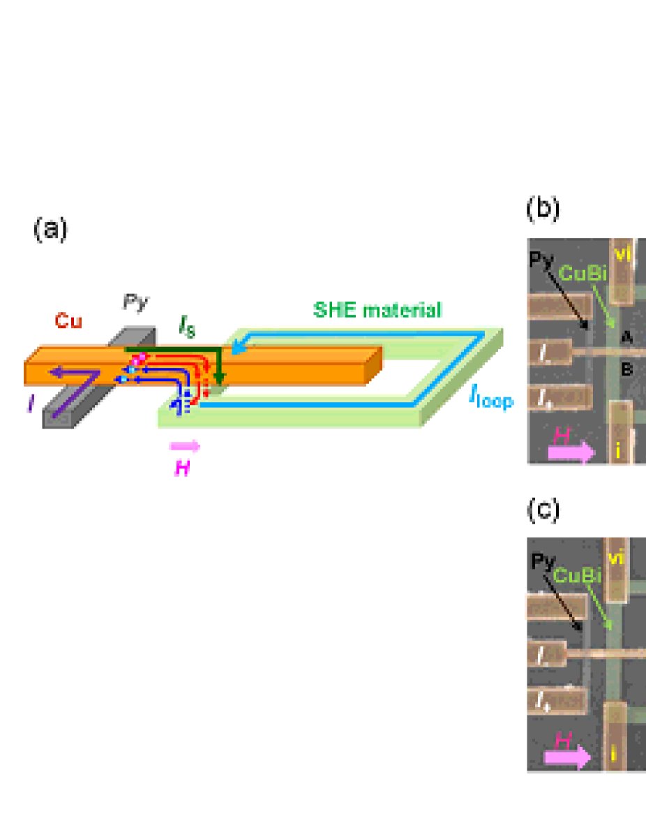
Samples have been fabricated on a thermally oxidized silicon subtrate using electron beam lithography on polymethyl-methacrylate resist and subsequent lift-off process. We first patterned a 100 nm wide wire and deposited permalloy (Py; Ni81Fe19) by 30 nm. We also patterned a closed loop or an open end shape next to the Py wire and deposited two different SHE materials, i.e., Cu99.5Bi0.5 and Pt, by 20 nm. The length of the loop is 6, 11, and 19 m, and the distance () between the Py wire and the SHE wire is 500 nm. The Py and SHE wires were bridged by a 100 nm wide and 100 nm thick Cu wire transferring the spin current. We also deposited six Cu electrodes (i-vi in Fig. 1) to measure the voltage () induced by the ISHE. Before the deposition of the Cu bridge and electrodes, a careful Ar ion etching was carried out for 30 seconds to obtain transparent interfaces between the SHE material and Cu as well as between Py and Cu. The detailed sample dimensions and other characteristics are listed in Table 1.
| Parameter | Py (F) | Cu (N) | Cu99.5Bi0.5 (M) | Pt (M) |
|---|---|---|---|---|
| (nm) | 100 | 100 | 250 | 200 |
| (nm) | 30 | 100 | 20 | 20 |
| (cm) | 19 | 1.5 | 11 | 14 |
| (nm) | 5 | 1300 | ||

In Fig. 1(a), we show the principle of ISHE in an SHE ring using the spin absorption method n.prl.2012 ; n.prl.2011 ; m.prb.2011 ; n.prb.2014 ; n.prl.2013 . When the electric current flows from the Py wire to the left side of the Cu wire, the resulting spin accumulation induces a pure spin current () on the right side of the Cu wire. The pure spin current is preferentially absorbed into the Cu99.5Bi0.5 or Pt ring. The opposite spin-up and spin-down electrons composing the absorbed pure spin current are deflected to the same direction by the ISHE. As we will detail later on, this conversion occurs only below the Cu bridge.
In the present work, we prepared two types of samples, i.e., closed loop circuit and open end one, as shown in scanning electron microscopy images in Figs. 1(b) and 1(c) and in schematics in Figs. 1(d) and 1(e). Figures 1(f) and 1(g) show ISHE resistances () of Cu99.5Bi0.5 measured with the closed loop and open end circuits, respectively. increases with increasing the magnetic field and is saturated above 2000 Oe, which is the saturation field of magnetization of the Py wire, as already shown in our previous reports m.prb.2011 ; n.prl.2011 ; n.prl.2012 ; n.prb.2014 . What is interesting to note is the amplitude of , i.e., . In the closed loop structure, depends on the distance between two voltage positions as shown in Fig. 1(f). For example, for m is about three times larger than that for m. Such a voltage position dependence of has never been observed in the normal open end circuit [see Fig. 1(g)].
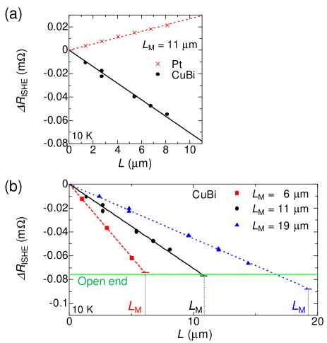
To see clearly the relation between and , we plot of the Cu99.5Bi0.5 and Pt rings as a function of in Fig. 2(a). Both of them show a linear dependence on , but of Cu99.5Bi0.5 has a negative slope while that of Pt has a positive one. This is consistent with our previous works; the SH angle of Cu99.5Bi0.5 is negative n.prl.2012 while that of Pt is positive m.prb.2011 . From the linear dependence of on , we can conclude that an electric current () flows in the SHE ring and the direction of the current relies on the SH angle of the SHE material. From the slope of vs curve, we can estimate in the ring; nA for Cu99.5Bi0.5 and for Pt when mA is applied. However, the obtained is too small when we simply consider the conversion of spin current into charge current via the ISHE.

We now formulate within the standard one-dimensional (1D) spin diffusion model t.prb.2003 . As shown in Figs. 1(d) and 1(e), the generated is absorbed into the SHE ring because of its strong spin-orbit interaction. In this device structure, the absorbed pure spin current can be expressed as follows:
| (1) |
where is defined as an average of pure spin current flowing vertically into the Cu99.5Bi0.5 or Pt ring. and are respectively the spin resistances of Cu, Py and Cu99.5Bi0.5 or Pt, and and . The spin resistance is defined as , where and are respectively the electrical resistivity, the spin diffusion length, the spin polarization, the effective cross sectional area involved in the equations of the 1D spin diffusion model and the suffix X represents each material (N, F or M). These values obtained at K are shown in Table 1.
The SH angle is the conversion rate between the pure spin current density and the charge current density . Thus, we obtain [see the red arrow in Figs. 1(d) and 1(e)]. For the open end case, no charge current flows in the circuit (i.e., ). This means that the converted charge current is compensated by and as depicted in Fig. 1(e): . Here , and are currents flowing in the SHE material only below the Cu bridge, in the Cu bridge, and in the SHE material outside the Cu bridge, respectively. As can be seen in Fig. 1(g), has no voltage position dependence. Thus, the induced ISHE voltage can be written as follows:
| (2) |
where is the resistance of the SHE material below the Cu bridge [see the caption of Fig. 1], is the longitudinal resistivity of the SHE material, and is the shunting factor, originally introduced in Ref. n.prl.2011 . This expression is indeed the same as Eq. (2) in Ref. n.prl.2011 .
In the loop structure, is not zero anymore as shown in Fig. 1(d) and can be expressed as:
| (3) |
To obtain Eq. (3), we assume . From this equation, we can explain that depends not only on but also on . In addition, at the endpoint of the loop () becomes Eq. (2) since it is a product of and the resistance of the loop. As is already obtained from Fig. 2, we can estimate with Eq. (3). We note that unlike the case of the lateral spin valve device n.prl.2012 ; n.prl.2011 ; m.prb.2011 ; n.prb.2014 , , which is needed to obtain , cannot be directly determined on the same device. Therefore, as shown in Table 1, we have referred to reported in our previous works n.prl.2012 ; n.prl.2013 to obtain ; for Cu99.5Bi0.5 and for Pt. These results are consistent with our previous works n.prl.2012 ; n.prl.2011 ; m.prb.2011 ; n.prb.2014 .

So far, we have fixed . To check Eq. (3), we prepared three different rings [see Fig. 2(b)]. As expected, depends on : for instance, becomes nA, for the Cu99.5Bi0.5 ring with m. Moreover, at the endpoint of the loop () coincides with of the open end circuit, as can be seen in Fig. 2(b). This result also supports the above consideration.
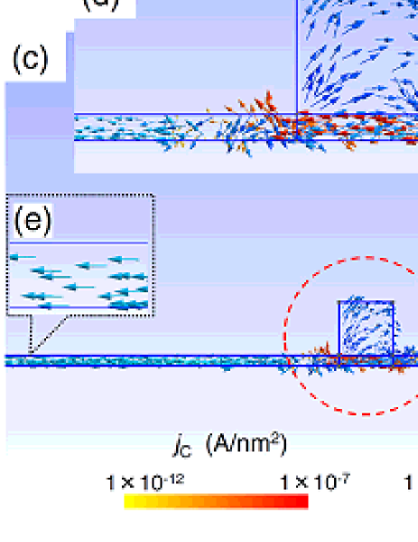
To confirm our 1D analysis, we have also performed three-dimensional (3D) analyses for and using SpinFlow 3D based on the Valet-Fert formalism n.prl.2012 ; v.prb.1993 . In the case of the open circuit device, the distribution of is homogeneous both for the left and right sides, and the difference between the two sides corresponds to , as shown in Fig. 3(a). This result also indicates that . When the SHE material has a closed loop structure, on the other hand, gradually changes from the positive value (on the left side) to the negative one (on the right side), but obtained at the two edges next to the Cu bridge is the same as that for the open end circuit [see Fig. 3(b)]. This is consistent with the experimental result shown in Fig. 2(b). To prove that the charge current flows in the ring, we show the charge current density distribution calculated with SpinFlow 3D in Figs. 3(c)-3(f). As in the case of the 1D model, is compensated by below the Cu bridge, but since the SHE material has a ring shape, the small leakage current flows in the ring. From the leakage current, we can also estimate by using shown in Table 1; for Cu99.5Bi0.5 and for Pt. These are again consistent with our previous works n.prl.2012 ; n.prb.2014 .
In Fig. 3, we selected Pt as an SHE material to show the current distribution in the ring. We obtain the similar current distribution for CuBi but with the opposite direction compared to Pt. However, the current distribution below the Cu bridge is much more complicated to see than that for Pt. This originates from the spreading of the spin accumulation at the side edges of the CuBi ring since is larger than n.prl.2012 .
Finally, we discuss how , and are generated in the closed loop circuit and how can be utilized. As shown in Fig. 1(d), the induced is injected into the SHE material from the Cu bridge. We note here that the conversion of into occurs only at the Cu/SHE-material junction. Thus, electrons converted from lose the driving force once they go out from the junction, and are accumulated to one side. This induces the electric field in the SHE wire. For the open end circuit, the accumulated electrons are balanced with the electric field, as in the case of the normal Hall effect. As a result, is cancelled out by and , and the electric voltage can be measured. When the circuit is closed, the electric field also induces in the loop. This is essentially different from a current due to electromotive force induced by an alternating magnetic field through a ring. Although we have used the ac lock-in technique to obtain , it is in principle a dc current. The present result clearly shows that by flowing from Py to Cu non-locally, another steady current can be induced in a mesoscopic ring with a large via the ISHE.
As discussed above, since is proportional to , it is of the order of 1 nA at the moment. By optimizing the device structure, the value can be enhanced by a factor of ten. Furthermore, by replacing a part of SHE ring with a superconductor, we could obtain a smaller resistance of the loop compared to the resistance of the shunt (Cu bridge). In such a case, should be enhanced closer to . It is known that when there is a magnetic flux threading such a mesoscopic ring, a small persistent current (of the order of 1 nA) is induced in the ring and shows an oscillation with a period of where is the Plank constant levy_prl_1990 ; webb_prl_1991 ; mailly_prl_1993 . In the same way as a dc-SQUID magnetometer, by arranging the SHE ring on top of a sample and measuring a current in the ring precisely, one could observe a modulation of and thus extract the magnetization of the sample.
In summary, we have measured the ISHEs of CuBi and Pt by means of the spin absorption technique in both open end and closed loop circuits, and found that the electric current can be obtained only in the closed loop. The detected current depends on the spin Hall angle of the SHE material and also on the resistance of the loop. It is commonly considered that the ISHE converts a spin current into a charge current, but this is the first observation of the converted charge current via the ISHE of CuBi or Pt. The amount of the charge current can be quantitatively explained by our spin transport models.
We acknowledge helpful discussions with T. Kato. We would also like to thank Y. Iye and S. Katsumoto for the use of the lithography facilities. This work was supported by KAKENHI (Grant No. 24740217 and 23244071) and by Foundation of Advanced Technology Institute.
References
- (1) S. Maekawa, Concepts in Spin Electronics (Oxford University Press, Oxford, 2006).
- (2) M. I. Dyakonov and V. I. Perel, Sov. Phys. JETP Lett. 13, 467 (1971).
- (3) J. E. Hirsch, Phys. Rev. Lett. 83, 1834 (1999).
- (4) T. Seki, Y. Hasegawa, S. Mitani, S. Takahashi, H. Imamura, S. Maekawa, J. Nitta and K. Takanashi, Nat. Mater. 7, 125 (2008).
- (5) L. Liu, C.-F. Pai, Y. Li, H. W. Tseng, D. C. Ralph, and R. A. Buhrman, Science 336, 555 (2012).
- (6) C.-F. Pai, L. Liu, Y. Li, H. W. Tseng, D. C. Ralph, and R. A. Buhrman, Appl. Phys. Lett. 101, 122404 (2012).
- (7) Y. Niimi, Y. Kawanishi, D. H. Wei, C. Deranlot, H. X. Yang, M. Chshiev, T. Valet, A. Fert, and Y. Otani, Phys. Rev. Lett. 109, 156602 (2012).
- (8) S. O. Valenzuela and M. Tinkham, Nature (London) 442, 176 (2006).
- (9) E. Saitoh, M Ueda, H. Miyajima, and G. Tatara, Appl. Phys. Lett. 88, 182509 (2006).
- (10) O. Mosendz, J. E. Pearson, F. Y. Fradin, G. E. W. Bauer, S. D. Bader, and A. Hoffmann, Phys. Rev. Lett. 104, 046601 (2010); O. Mosendz, V. Vlaminck, J. E. Pearson, F. Y. Fradin, G. E. W. Bauer, S. D. Bader, and A. Hoffmann, Phys. Rev. B 82, 214403 (2010).
- (11) Y. Niimi, M. Morota, D. H. Wei, C. Deranlot, M. Basletic, A. Hamzic, A. Fert, and Y. Otani, Phys. Rev. Lett. 106, 126601 (2011).
- (12) M. Morota, Y. Niimi, K. Ohnishi, D. H. Wei, T. Tanaka, H. Kontani, T. Kimura, and Y. Otani, Phys. Rev. B 83, 174405 (2011).
- (13) Y. Niimi, D. Wei, H. Idzuchi, T. Wakamura, T. Kato, and Y. Otani, Phys. Rev. Lett. 110, 016805 (2013).
- (14) Y. Niimi, H. Suzuki, Y. Kawanishi, Y. Omori, T. Valet, A. Fert, and Y. Otani, Phys. Rev. B. 89, 054401 (2014).
- (15) S. Takahashi and S. Maekawa, Phys. Rev. B 67, 052409 (2003); Sci. Tech. Adv. Matter. 9, 014105 (2008).
- (16) T. Valet and A. Fert, Phys. Rev. B. 48, 7099 (1993).
- (17) L. P. Lévy, G. Dolan, J. Dunsmuir, and H. Bouchait, Phys. Rev. Lett. 64, 2074 (1990).
- (18) V. Chandrasekhar, R. A. Webb, M. J. Brady, M. B. Ketchen, W. J. Gallagher, and A. Kleinsasser, Phys. Rev. Lett. 67, 3578 (1991).
- (19) D. Mailly, C. Chapelier, and A. Benoit, Phys. Rev. Lett. 70, 2020 (1993).