General analytical solutions for DC/AC circuit network analysis
Abstract
In this work, we present novel general analytical solutions for the currents that are developed in the edges of network-like circuits when some nodes of the network act as sources/sinks of DC or AC current. We assume that Ohm’s law is valid at every edge and that charge at every node is conserved (with the exception of the source/sink nodes). The resistive, capacitive, and/or inductive properties of the lines in the circuit define a complex network structure with given impedances for each edge. Our solution for the currents at each edge is derived in terms of the eigenvalues and eigenvectors of the Laplacian matrix of the network defined from the impedances. This derivation also allows us to compute the equivalent impedance between any two nodes of the circuit and relate it to currents in a closed circuit which has a single voltage generator instead of many input/output source/sink nodes. Contrary to solving Kirchhoff’s equations, our derivation allows to easily calculate the redistribution of currents that occurs when the location of sources and sinks changes within the network. Finally, we show that our solutions are identical to the ones found from Circuit Theory node analysis.
pacs:
41.20.-q,89.75.Hc,45.30.+s,95.75.PqI Introduction
The currents in each edge of an electrical circuit, which is composed of linear elements (i.e., resistance, capacitance, and inductance) and where conservation of charge at each node is granted, are generally found by solving Kirchhoff’s equations Kirchhoff . In particular, for resistor networks, the solution for the currents at each edge is related to random walks in graphs FanChung1997 , first-passage times Randall2006 , finding shortest-paths and community structures on weighted networks Newman2004 , and network topology spectral characteristics Rubido2013a ; Rubido2013b . Though the relationship between currents and voltage differences in network circuits with linear elements follows Ohm’s law, their modelling capability is enormous. For example, it is used to model fractures in materials Batrouni1998 , biologically inspired transport networks Katifori2010 , airplane traffic networks Bocaletti2013 , robot path planing Zuojun2006 , queueing systems Haenggi2002 , etc.
In practice, resistor networks are used in various electronic designs, such as current or voltage dividers, current amplifiers, digital to analogue converters, etc. These devices are usually inexpensive, relatively easy to manufacture, and require little precision on the constituents. In order to solve the voltages across these networks, two methods are broadly used: nodal analysis and mesh analysis Kirchhoff . In the former, nodes are labelled arbitrarily and voltages are set by using the Kirchhoff’s current equations of the system. In the later, loops are defined with an assigned current which do not contain any inner loop, then the Kirchhoff’s voltage equations are solved. These constitute classic techniques of Circuit Theory.
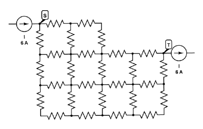
However, nodal and mesh methods (or even transfer function methods Ali2010 ) become inefficient to recalculate the voltage drops across the network if the location of inputs and outputs changes constantly, e.g., if the cathode and/or anode of a voltage generator are moved from one node of the network to another. This switching situation is common in the modelling of the modern power-grid as an impedance network circuit or in general supply-demand networks Rubido2013a ; Rubido2013b ; Batrouni1998 ; Katifori2010 . An example of this case is shown in Fig. 1 for a resistor network with a single source-sink nodes. Another redistribution of currents, which is also poorly accounted by these methods, happens if a single source node and single sink node are decentralized for multiple source and/or multiple sink nodes that preserve the initial input and output magnitudes Batrouni1998 ; Renatas2013 . In any case, either of the classical Circuit Theory methods requires to be applied for each configuration of the sources and sinks in order to find the currents at every edge of the network.
In this work, we present novel general analytical solutions for current conservative DC/AC circuit networks with resistive, capacitive, and/or inductive edge characteristics. The novelty comes from expressing the currents and voltage drops in terms of the eigenvalues and eigenvectors of the admittance (namely, the inverse of the edge impedance) Laplacian matrix of the circuit network.
In order to derive our novel solutions we assume that the impedance values at every edge and the location of the source/sink nodes are known. Our solutions give the exact DC/AC currents that each edge of the circuit holds and are identical in magnitude to the ones found from nodal Circuit Theory analysis. The practicality of our solutions comes from, allowing to compute the equivalent impedance between any two nodes of the network directly Cserti2000 ; Wu2004 ; Jason2012 and allowing to easily calculate the redistribution of currents that happens when the location of sources and sinks is changed within the network (such as in the example of Fig. 1). The scientific interest of our solutions comes from, establishing a clear relationship between the currents and voltages in DC/AC circuits with the topology invariants of the network, namely, its eigenvalues and eigenvectors.
(a)
(b)

The approach we develop provides new analytical insight into the transmission flow problem and exhibits different features than other available solutions. Moreover, it provides a new tool to achieve the voltage/current solutions and to analyse resonant behaviour in linear circuits Silva2013 . As a practical application, we relate these solutions to closed circuits where a voltage generator is present (instead of having open sources/sinks that feed current to the network) and solve a simple network where we can compare our solutions to the ones provided by solving directly Kirchhoff’s nodal equations.
II DC/AC circuit networks
II.1 The mathematical model
The model we solve corresponds to a conservative circuit network with known input/output net currents and obeys Ohm’s and Kirchhoff’s law for conservation of charge. We assume that the input (output) net current () at the source (sink) node (), its frequency (with for DC currents and for AC currents), and their phases are known. The extension to various input or output nodes is done in Appendix C.
Ohm’s law linearly relates the current at an edge of the circuit with the voltage difference between the nodes that the edge connects. Specifically,
| (1) |
where is the current passing from node to node given a current source located at node and a sink node located at node , is the voltage difference, and is the impedance of the symmetric edge. depends on the edge’s resistive, capacitive, and/or inductive properties, and the network topological properties of the circuit.
The variables in Eq. (1) are complex numbers in the case of AC input/output currents and real numbers for DC currents. In general, a resonance in the -edge appears for a minimum of the impedance, namely, when the input/output frequency is tuned to a frequency related to the natural frequency of the edge line. For example, in the case that the edge is modelled by a series circuit, the impedance of the edge is
| (2) |
where is the natural frequency of the edge, is the dissipation of the edge, is the edge’s inductance, is the edge’s capacitance, is the edge’s resistance, and . In this case, a resonance in the -edge appears if . Consequently, our solutions are valid as long as the input/output frequency is different from any of the resonant frequencies associated to the edges of the network.
The topological properties of the network are also included in the value of the impedance of each edge. For instance, the impedance between two nodes that are not connected is assumed to be because for a non-existing line. Otherwise, the impedance of two connected nodes is . Hence, the inverse of the impedance defines a complex valued adjacency matrix, i.e., it gives which are the edges connecting the nodes in the circuit and their weights.
Kirchhoff’s law of conservation of charge states that current is conserved at every node in the circuit. In other words, the inflow equals the outflow at a node, with the exception of the source and sink nodes (the extension to multiple sources and sinks is detailed in Appendix C). Specifically,
| (3) |
where () is the complex valued net current inflow (outflow) and () is the Kronecker delta function. By assuming local conservation of charge at every node of the circuit, we get that the total flow in the network needs to be null, namely, global conservation of charge holds: , which is fulfilled only if .
Using Eqs. (1) and (3), the model equations are
| (4) |
which are expressed in matrix form as
| (5) |
where is the weighted admittance Laplacian matrix of the network [with complex entries given by ], is the inflow/outflow vector (with non-zero entries only at node , , and at node , ), and is the voltage potential at each node of the network. Properties of the weighted Laplacian matrix are dealt in Appendix A.
II.2 The analytical solutions
We are deriving two main analytical results in this work. An expression for the DC/AC currents flowing through each edge of the network (as function of the location of the source and sink nodes and the net inflow magnitude) and the equivalent impedance between any two nodes of the network. Both results are expressed in terms of the eigenvalues and eigenvectors of the Laplacian matrix of Eq. (5), and are found from the inversion of (see Appendix B for details on the inversion of ).
We find that after the inversion of the voltage difference between any two nodes of the circuit is given by
| (6) |
where is the complex -th eigenvalue of Laplacian (with and FanChung1997 ) and is the corresponding -th eigenvector coordinate (with ). With the exception of (assuming the phase difference between the net input and output flows is null, which guarantees global charge conservation), the remaining quantities are complex numbers, hence, they have an amplitude and a phase, and the indicates complex conjugation. Thus,
| (7) |
where [] is the real [imaginary] part of the product and the phases are
| (8) |
with [] being the -th eigenvalue of the real [imaginary] part of the Laplacian matrix (details on the properties of these eigenvalues are provided in Appendix A).
Our first main analytical result is the current passing through the -edge, namely,
| (9) |
where , being the impedance phase value. This phase also corresponds to the phase difference between the voltage drop between nodes and and the current at the -edge.
Setting the source at node and the sink at node , Eq. (6) results in
| (10) |
and the second main analytical result is derived, i.e.,
| (11) |
is the effective weight that all edges linking node with weigh Wu2004 ; Rubido2013a ; Rubido2013b , namely, the equivalent impedance. Its value is identical to the ones obtained by using Green functions Cserti2000 or Circuit Theory analysis Kirchhoff . For example, if all series and parallel impedances between nodes and are added, then the final value is equal to the one that is found from Eq. (11).
II.3 Practical examples
Here we show how to relate the solution found so far [Eq. (9)] for the currents in the edges of a network-like circuit for given input/output nodes with the currents in the edges of a closed circuit with a single voltage generator. As it is known, solutions for closed linear circuits with given boundary voltage values correspond to finding solutions of the Laplace equation without sources, which are widely known. Hence, finding a relationship between Eq. (9) with the closed circuit currents, in our case, is equivalent to finding a relationship between topological invariant properties of the network structure (impedances) with Laplace boundary problem solutions.
(a)

(b)
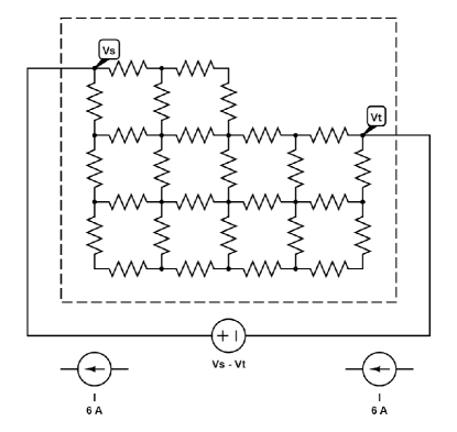
For a single source-sink problem [like the one depicted in Fig. 2(a)] to be transformed to a Laplace problem [Fig. 2(b)], the source and sink nodes ( and ) are plugged into a voltage generator. The known data from the source-sink problem is the fixed input net current , which the generator will need to provide to the network circuit between nodes and . Hence, the voltage requirement for the generator to supply is: , where is the equivalent resistance between the nodes and of the known network circuit structure [dashed square in Fig. 2(b)]. The equivalent resistance is found from Randall2006 ; Rubido2013a ; Rubido2013b
| (12) |
where () is the real -th eigenvalue (eigenvector) of the resistor network Laplacian matrix (which is also positively defined because its entries are all real valued). Equation (12) is the resistive version of Eq. (11). Then, the corresponding identical Laplace problem to the single source-sink pair of nodes is solved for the border conditions corresponding to a voltage generator supplying a constant voltage difference between nodes and of magnitude
| (13) |
where is the node and edge set which define the circuit network. Equation (13) establishes a direct relationship between solving Laplace problems in circuits with transportation problems. Consequently, this relationship increases the importance of our voltage solution in terms of the Laplacian matrix eigenvalues and eigenvectors.
As another practical example, we compare our solutions for a square-like resistor network with equal edges with the solutions found from linear Circuit Theory analysis. We index the nodes in the square as in clockwise direction and the edge’s resistances as . Setting an input (output) source (sink) at node () with magnitude (), nodal analysis gives the following results for the edge currents that this circuit system has: and . Also, the resultant equivalent resistance between nodes and for the square is given by
| (14) |
In our framework, we transform the resistor network into a topological problem, i.e., we analyse the Laplacian matrix of the network. Applying Ohm’s and Kirchhoff’s laws, a square-like resistor network has the following conductance matrix [see Eq. (5)]
| (15) |
where the first column/row corresponds to node , then node , node , and finally node . The eigenvalues of are , , and , and the eigenvectors are , , , and . Thus, using Eq. (6) for the edge current between nodes and , we have
that results in
| (16) |
where the other eigenvector modes in the sum are cancelled or have null coordinates. Similarly, the remaining edge currents are calculated and found identical to the ones from nodal analysis. Moreover, the equivalent resistance we calculate for nodes and using Eq. (12) is
| (17) |
which again, is identical to the one in Eq. (14).
We can extend this problem easily for the case where the square circuit has equal impedances in every edge, where is the characteristic frequency of each edge and is the input frequency (, for every time ). Then, the admittance Laplacian matrix entries from Eq. (5) are given by
| (18) |
The inverse of the impedance (admittance) is given by
| (19) |
where if node is connected to node , otherwise, and . The resultant admittance Laplacian matrix in this case is
| (20) |
with () being the real (imaginary) part of the entries in Eq. (18) and the Laplacian matrix from Eq. (15). Consequently, the eigenvalues of are simply the eigenvalues of divided by the impedance and these matrices share the same eigenvectors.
In this case (the square circuit with identical impedances for its edges), the AC current flowing between nodes and is
| (21) |
which is the same result as in the equal resistances DC case [Eq. (16)] for the modulus because . Furthermore, the analogy is further seen when calculating the equivalent impedance between the source () and sink () nodes using Eq. (11). This results in
| (22) |
The solution is identical to the one that Circuit Theory derives and is in direct correlation with the DC problem as expected.
In more general scenarios, the relationship between the DC and AC circuit is not direct. In such situations, the complex entries of the Laplacian matrix for the AC case are not related to the DC Laplacian matrix. Hence, further assumptions need to be done to find analytical solutions. For instance, one could have to impose that the input frequency to be larger than the natural frequencies of the lines ( for every edge), such that the imaginary part of the Laplacian be positive semi-defined (see Appendix A).
III Conclusions
The approach we develop provides new analytical insight into the transmission flow problem and exhibits different features than other available solutions. Moreover, it provides a new tool to achieve the voltage/current solutions and to analyse resonant behaviour in linear circuits. As a practical application, we relate these solutions to closed circuits where a voltage generator is present (instead of having open sources/sinks that feed current to the network) and solve a simple network where we can compare our solutions to the ones provided by solving directly Kirchhoff’s equations. Our findings help to solve problems, where the input and output nodes change in time within the network, more effectively than classical Circuit Theory techniques.
Appendix A Complex weighted Laplacian matrix characteristics
The weighted Laplacian matrix of the circuit network with edge properties given by the symmetric line impedances has the following complex value entries
| (23) |
hence,
| (24) |
which is the first requirement for a Laplacian matrix: the zero row sum property.
The eigenspace of is composed of a set of complex eigenvalues and eigenvectors with , such that
thus,
| (25) |
where is a unitary matrix (, being the identity matrix) of eigenvectors and is a diagonal matrix of eigenvalues ().
Due to Eq. (24), has a null eigenvalue (referred to as in the following) associated to the kernel vector , where . Using Eq. (24), . Hence, the kernel of the matrix (the space of eigenvectors associated to the null eigenvalues) is at least of dimension and direct inversion of the matrix is not possible. This is the second property of a Laplacian matrix,
| (26) |
which implies that the rank of the matrix is less than .
The third property is that Laplacian matrices are positive semi-defined. In particular, for any column vector , the Dirichlet sum is such that
| (27) |
where “” is the inner product operation and is the weighted adjacency matrix of the circuit network. This inequality holds only if for all and . As a consequence, it implies that all eigenvalues are non-negative, because can be any of the eigenvectors. In that case,
where the last equality is possible because of the unitary property of the eigenvectors (). However, Eq. (27) is always valid only for Laplacian matrices with non-negative real entries.
For complex entries, such as in our , the inequality in Eq. (27) can be analysed by splitting the matrix into a real () and an imaginary () part, i.e., , where
| (28) |
| (29) |
and . The Laplacian matrix contains the information of the network structure resistive part and the Laplacian matrix contains the information of the network structure reactive part. In other words, the dissipative and the resonant structure of the circuit network, respectively.
In order to have a positive (or negative) semi-defined Laplacian matrix, the weighted adjacency matrix elements need to be positive (or negative) for all pairs of nodes. For example, for the real part, if , then is positive semi-defined. Consequently, the validity of this property depends on the magnitude of the phases that the impedance of the lines introduce. In particular, for lines that can be modelled by series , the for every -edge, hence, has a non-negative spectra of eigenvalues. However, in such a case, the sign of depends on the input/output frequency [see Eq. (2)]. For for all -edges, , thus has a non-negative spectra of eigenvalues as . For , , thus, the opposite happens.
In general, in our case a rule of thumb for knowing the character of the spectra of the matrix is missing (the elements are complex and are not bounded solely to the positive quadrant of the complex plane). However, the unitary base property of the set of associated eigenvectors is always valid. This means that
| (30) |
and
| (31) |
Equation (30) is the verification that the eigenvector set is composed solely by linearly independent vectors. Equation (31) is the completeness property, and it is the verification that the set is also a generating set. Hence, it conforms a basis of the linear functions that operate over the set of nodes.
Appendix B Inversion of the Laplacian matrix and the node Voltage Potential solutions
Due to the existence of the null eigenvalue in any Laplacian matrix, the inverse is ill defined. We overcome this problem by means of a translation in Eq. (5) and the removal of the kernel from the eigenvector base. Namely,
| (32) |
where all entries of matrix are equal to unity () and for all is the vector components resultant of the product between and .
From Eq. (25) we know we can write the elements of the Laplacian in terms of its complex eigenvalues and eigenvectors by
| (33) |
where the term corresponding to has been removed because . In a similar fashion we define the following matrix entries
| (34) |
Here we show that is the inverse matrix of . In a sense, is a matrix with elements that represent the conductivity of the edges, whereas represents the impedance of the edges. First, we note that , hence, . Then, we observe that because of the zero row sum property. Similarly, . This is seen from,
However, as Eq. (30) holds for every eigenvector of , in particular, , then for every spanning eigenvector (). Finally,
where, using Eq. (30), it results in
| (35) |
Now, observing that Eq. (31) can be written as
then, Eq. (35) is further simplified
| (36) |
Consequently, we have shown that
| (37) |
Returning to Eq. (32), and using Eq. (37), we obtain the voltage potentials at each node
| (38) |
where we use that and . If global conservation of charge is granted, namely, if the input current equals the output current in phase and magnitude, then, . Otherwise, is a vector with all the elements equal to the magnitude and/or phase difference between the input and output net currents [see Eq. (3)]. We note that the role of in Eq. (38) is to add an arbitrary constant to the node voltage potential. This is easily interpreted as the arbitrary energy reference point. Such arbitrary value is eliminated once voltage differences are calculated. Moreover, voltage differences eliminate also the possible constant value given by . Consequently, the voltage difference between two arbitrary nodes and in the network is given by
| (39) |
Thus,
Appendix C Many input/output flows and the relationship to voltage generators
In order to analyse how Eq. (39) changes when many sources and sinks are present, we need to rewrite Eq. (3) to include the new sources of inflow and sinks of outflow. Thus, in general, the net current at a node is
| (40) |
where () is the set of nodes that act as sources (sinks) and () is the fraction of the total inflow (outflow) that goes through node (), namely, (). Consequently, global conservation of charge is granted. Substituting Eq. (40) into Eq. (39), the voltage difference between nodes and in the circuit network with multiple sources and sinks is
| (41) |
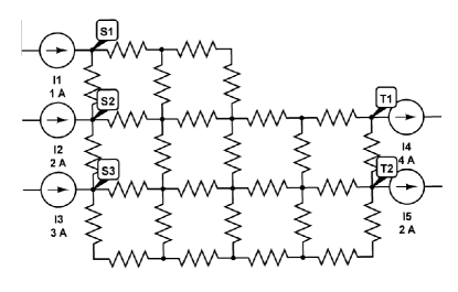
(a)
(b)
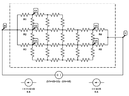
When multiple sources and sinks exist [e.g., panel (a) in Fig. 3], then the transformation of the problem to a closed circuit problem requires the inclusion of a single super source node and super sink node need to be created [panel (b)]. All original source (sink) nodes are then connected to the new super source (sink) node that provides the total input (output) that the multiple sources (sinks) were feeding (consuming) in the original system , namely, (). Consequently, the multiple source-sink configuration in is transformed into a single - pair configuration of a new network that has nodes more than the original network . In such conditions, the former process enables to analyse the new network setting by means of a single generator that connects these two new nodes. In other words, once a super source (sink ) that connects to all the original sources (sinks ) is defined, then a Laplace problem can be defined by setting a voltage generator which provides
| (42) |
where the equivalent resistance between the super source and super sink is unknown. This is because the impedance (resistance) values for the new edge connections between the multiple sources (sinks ) to the super source [which have to be set such that the current entering the network circuit through the old multiple sources (sinks) is identical to the one the particular source (sink) supplies (consumes), e.g., as in panel (b) of Fig. 3] are unknown.
In order to determine the impedances (resistances) of the edges connecting the super source (sink) to the multiple source (sink) nodes, we observe that:
where neither the voltages nor the resistances are known. Nevertheless, the voltages of the super nodes fulfil Eq. (42), thus, arbitrarily setting the unknown resistances for the new edges to unity, can be derived and the node voltages for each of the multiple sources and sinks calculated. That is,
| (43) |
Acknowledgement
The authors thank the Scottish University Physics Alliance (SUPA).
References
- (1) P. R. Clayton, Fundamentals of electric circuit analysis (Wiley, 2001).
- (2) F. R. K. Chung, Spectral Graph Theory (American Mathematical Soc. and CBMS 92, 1997).
- (3) D. Randall, “Rapidly mixing Markov chains with applications in computer science and physics”, Computing in Science & Engineering, vol. 8, no. 2, pp 30-41, 2006.
- (4) M. E. J. Newman and M. Girvan, “Finding and evaluating community structure in networks”, Phys. Rev. E, vol. 69, no. 026113, 2004.
- (5) N. Rubido, C. Grebogi, and M. S. Baptista, “Structure and function in flow networks”, Europhys. Lett., vol. 101, no. 68001, 2013.
- (6) N. Rubido, C. Grebogi, and M. S. Baptista, “Resiliently evolving supply-demand networks”, Phys. Rev. E, vol. 89, no. 012801, 2014.
- (7) G. G. Batrouni, and A. Hansen, “Fracture in Three-Dimensional Fuse Networks”, Phys. Rev. Lett., vol. 80, no. 325, 1998.
- (8) E. Katifori, G. J. Szollosi, and M. O. Magnasco, “Damage and Fluctuations Induce Loops in Optimal Transport Networks”, Phys. Rev. Lett., vol. 104, no. 048704, 2010.
- (9) A. Cardillo, M. Zanin, J. Gómez-Gardeñes, M. Romance, A. J. García del Amo, and S. Boccaletti, “Modeling the multi-layer nature of the European Air Transport Network: Resilience and passengers re-scheduling under random failures”, Eur. Phys. J. Special Topics, vol. 215, pp 23-33, 2013.
- (10) Z. Liu, S. Pang, S. Gong, and P. Yang, “Robot Path Planning in Impedance Networks”, Proc. of 6th World Congress on Intelligent Control and Automation, vol. 2, pp 9109-9113, 2006.
- (11) M. Haenggi, “Analogy between data networks and electronic networks”, Electronic Letters, vol. 38, no. 12, pp 553-554, 2002.
- (12) A. Hajimiri, “Generalized Time- and Transfer-Constant Circuit Analysis”, IEEE Trans. Circuits Syst. I: Regular Papers, vol. 57, no. 6, pp 1105-1121, 2010.
- (13) R. Jakushokas and E. G. Friedman, “Power Network Optimization Based on Link Breaking Methodology”, IEEE Trans. on very large scale Int. (VLSI) Syst., vol. 21, no. 5, pp 983-987, 2013.
- (14) J. Cserti, “Application of the lattice Green’s function for calculating the resistance of infinite networks of resistors”, Am. J. Phys., vol. 68, no. 10, pp 896-906, 2000.
- (15) F. Y. Wu, “Theory of resistor networks: the two-point resistance”, J. Phys. A: Math. Gen., vol. 37, pp 6653-6673, 2004.
- (16) J. Zheng Jiang and M. C. Smith, “Series-Parallel Six-Element Synthesis of Biquadratic Impedances”, IEEE Trans. Circuits Syst. I: Regular Papers, vol. 59, no. 11, pp 2543-2554. 2012.
- (17) F. G. S. Silva, R. N. de Lima, R. C. S. Freire, and C. Plett, “A Switchless Multiband Impedance Matching Technique Based on Multiresonant Circuits”, IEEE Trans. Circuits Syst. II: Express Briefs, vol. 60, no. 7, pp 417-421, 2013.