Modeling of Lead Halide Perovskites for Photovoltaic Applications
Abstract
We report first-principles calculations, using the full potential linear augmented plane wave method, on six lead halide semiconductors, namely, CH3NH3PbI3, CH3NH3PbBr3, CsPbX3 (XCl, Br, I), and RbPbI3. Exchange is modeled using the modified Becke-Johnson potential. With an appropriate choice of the parameter that defines this potential, an excellent agreement is obtained between calculated and experimental band gaps of the six compounds. We comment on the possibility that the cubic phase of CsPbI3, under hydrostatic pressure, could be a topological insulator.
I I. INTRODUCTION
Recently, materials with halide perovskite structure, with the general formula ABX3, have attracted great interest, primarily because of their potential applications as light harvesters in solar cells 1 and as topological insulators.2; 3 Many studies have ensued with the aim of both improving the performance of these materials in photovoltaic cells and of understanding which physical parameters may determine the efficiencies.4; 5; 6; 7; 8; 9; 10; 11; 12; 13; 14; 15; 16; 17; 18; 19 For example, Lee et al.16 report a solution-processable solar cell which uses a perovskite of mixed halide form, namely methylammonium lead iodide chloride, CH3NH3PbI2Cl (abbreviated as MAPbI2Cl), with a solar-to-electrical power conversion efficiency of 10.9%. Using chemically-tuned MAPb(I(1-x)Brx)3 perovskites as light harvesters, a mesoporous titanium dioxide (TiO2) film, and a hole-conducting polymer, Noh et al. 17 demonstrate solar cells with a 12.3% power conversion efficiency. Burschka et al. 18 describe a sequential deposition method whereby MAPbI3 nanoparticles are formed within porous TiO2, resulting in a power conversion efficiency of 15%. Liu et al. 19 have subsequently shown that such nanostructuring is not necessary for high efficiencies; a planar heterojunction solar cell, with a deposited thin film of MAPbI2Cl acting as a light absorber, can achieve an efficiency exceeding 15%.
MAPbI3 and similar compounds are derived from a class of trihalide perovskite structures with the formula ABX3 (A=Cs, Rb; B=Pb; X=Cl, Br, I) by replacing the alkali-metal atom with methylammonium (MA). Such a replacement causes a large downshift in the semiconducting energy gap, making the compounds useful for photovoltaic applications. It is anticipated that different band gaps may be obtained by replacing methylammonium with other entities such as NH4 or CH2CH, by applying pressure, or by using thin films consisting of only a few layers.
To maximize the usefulness of such materials in photovoltaic applications, it is important to begin by developing computational techniques that accurately describe their electronic structure. Density functional theory in the Kohn-Sham formulation 20 is the most widely-used method. Here, the exchange-correlation potential is approximated by a functional of the electronic density. The most common approximations are the local density approximation (LDA),20 the generalized gradient approximation (GGA),21 and the hybrid approximation.22 While LDA and GGA provide a successful description of ground-state properties in crystals, this success does not extend to a description of excited states. In many semiconductors, LDA and GGA strongly underestimate the value of the energy gap. Improved values for the band gaps are usually obtained by using the GW method.23 However, the high computational cost of this method limits its applicability to crystals with a small number of atoms in the unit cell.
An exchange potential was recently proposed by Becke and Johnson (BJ), designed to yield the exact exchange potential in atoms.24 Unfortunately, the use of this potential led to a slight improvement in the energy gap values for many semiconductors.25 A simple modification of the BJ potential was proposed by Tran and Blaha.26 In this method, known as TB-mBJ, the exchange potential is given by
| (1) |
where
| (2) |
is the electron density ( is the number of occupied orbitals and is the Kohn-Sham (KS) orbital wave function),
| (3) |
is the KS kinetic energy density, and
| (4) |
is the Becke-Roussel exchange potential.27 The function in the above equation is determined by a nonlinear equation involving , , , and . Once is found, is determined by
| (5) |
In the TB-mBJ potential given in Eq (1),
| (6) |
where
| (7) |
is the average of over the unit cell of volume . The parameters and bohr1/2 were chosen because they produce the best fit to the experimental band gaps of many semiconductors. Studies have shown that the TB-mBJ potential is generally as accurate in predicting the energy gaps of many semiconductors as the much more expensive GW method.28
Despite its many successes, however, the performance of the TB-mBJ method is not very satisfactory in certain cases, especially for transition metal oxides. To improve the band gap prediction, Koller, Tran, and Blaha 29 consider a more general form for c,
| (8) |
They vary the values of parameters , , and in order to improve the quality of the fit between the calculated and the experimental energy gaps of many semiconductors. There is an overall improvement in predicting the energy gaps of semiconductors with moderate gaps when , , and . The modified BJ method employing these values for , , and will be referred to as the KTB-mBJ method. It should be pointed out that, in terms of computational time and resources, the requirements for the TB-mBJ and KTB-mBJ methods are essentially the same as those for standard LDA or GGA methods. Therefore, these methods may be easily used to calculate the electronic structure of crystals with large unit cells, where the cost of the GW method is prohibitive.
In this work, we present first-principles calculations on the electronic structure of six compounds, namely MAPbI3, MAPbBr3, CsPbX3 (X=Cl, Br, I), and RbPbI3. All of these compounds have a perovskite structure, characterized by a Pb atom that is octahedrally coordinated to six halogen atoms. We show that GGA, when spin-orbit coupling (SOC) is included, severely underestimates the band gaps in these semiconducting materials. Though TB-mBJ and KTB-mBJ methods lead to significant improvement in the values of the gaps, both methods still underestimate the energy gaps by a wide margin. We then show that keeping parameters and essentially the same as in TB-mBJ, while adopting a new value for leads to results that are in excellent agreement with experimental values.
II II. METHODS
Total energy and band structure calculations are carried out using the all-electron, full potential, linear augmented plane wave (FP-LAPW) method as implemented in the WIEN2k code.30 Here, each atom is surrounded by a muffin-tin sphere, and the total space is divided into two regions. One region consists of the interior of these nonoverlapping spheres, while the rest of the space constitutes the interstitial region. The radii of the muffin-tin spheres are 2.5 for Cs, Rb, Pb, I, and Br, 2.37 for Cl, 1.27 for N, 1.33 for C, and 0.68 for H, where is the Bohr radius. In GGA calculations, the exchange correlation potential is that proposed in reference.21
The valence electrons’ wave functions inside the muffin-tin spheres are expanded in terms of spherical harmonics up to . In the interstitial regions, they are expanded in terms of plane waves, with a wave vector cutoff of . Because of the small muffin-tin radius of hydrogen atoms, we set in CH3NH3PbI3 and CH3NH3PbBr3, where is the muffin-tin radius of the H atom. In the remaining four compounds, we set , where is the smallest muffin-tin radius. The charge density is Fourier expanded up to a maximum wave vector of , where for MAPbI3 and MAPbBr3, and for the remaining compounds. The convergence of the self-consistent calculations is achieved with a total energy tolerance of 0.1 mRy and a charge convergence of 0.001 e.
III III. RESULTS AND DISCUSSION
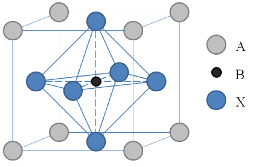
At high temperatures, lead halide perovskites have a simple cubic unit cell, where Pb sits at the center of the cube and is octahedrally coordinated to six halogen atoms, while alkali atoms sit at the cube corners, as shown in Fig. 1. As the temperature is lowered, distortions lead to tetragonal and/or orthorhombic structures. In our calculations, we use the room temperature crystal structures of the various compounds. These are listed in Table 1. For CsPbI3, which is orthorhombic at room temperature, we also study the high temperature cubic phase, which was predicted to be a topological insulator when subjected to hydrostatic pressure.2
| Compound | Structure | Lattice constants (Å) |
|---|---|---|
| CH3NH3PbI3 | Tetragonal | a=8.856, c=12.655a |
| CH3NH3PbBr3 | Cubic | a=5.933b |
| CsPbCl3 | Cubic | a=5.605c |
| CsPbBr3 | Orthorhombic | a=8.244, b=11.735, c=8.198d |
| RbPbI3 | Orthorhombic | a=10.276, b=4.779, c=17.393e |
| CsPbI3 | Orthorhombic | a=10.458, b=4.801, c=17.776e |
| CsPbI3 | Cubic | a=6.2894e |
We carried out band structure calculations on the six compounds shown in Table 1. Using GGA, we found that, upon including the effect of SOC, the band gaps of all compounds are severely underestimated. The values of the gaps are improved by using the TB-mBJ method, and are improved further by using the KTB-mBJ method. However, the improvement does not go far enough, and the gaps are still far below the experimental values. We thus considered a new set of values for the parameters that appear in Eq. (8), namely,
| (9) |
The parameters and are essentially the same as in the TB-mBJ method, but the parameter is different. With this new set of values for , , and , the calculated band gaps of all six compounds are in excellent agreement with the experimental values. Our results are summarized in Table 2 where we present the band gaps calculated by using different methods. The gaps obtained by using the above values for , , and are given in the column labeled ’Present method.’
| Compound | GGA | GGA+so | TB-mBJ | KTB-mBJ | Present method | Experimental |
|---|---|---|---|---|---|---|
| CH3NH3PbI3 | 1.492 | 0.377 | 0.844 | 0.921 | 1.544 | 1.5-1.6[a,b] |
| CH3NH3PbBr3 | 1.668 | 0.453 | 1.183 | 1.406 | 2.233 | 2.28[a] |
| CsPbCl3 | 2.498 | 0.707 | 1.585 | 1.889 | 2.829 | 2.86[c] |
| CsPbBr3 | 1.794 | 0.669 | 1.316 | 1.461 | 2.228 | 2.24[c,d] |
| RbPbI3 | 2.468 | 1.828 | 2.387 | 2.446 | 3.302 | 3.17[e] |
| CsPbI3 | 2.504 | 1.876 | 2.426 | 2.476 | 3.330 | 3.14[e] |
| CsPbI3 (cubic) | 1.324 | 0.072 | 0.485 | 0.529 | 1.072 | - |
The calculated energy bands of MAPbI3 along high symmetry directions in the Brillouin zone (BZ), in addition to the electronic density of states, are presented in Fig. 2. The valence band maximum (VBM) and conduction band minimum (CBM) occur at the -point, the BZ center. In cubic perovskites, the gap occurs at point R(1/2, 1/2, 1/2). However, at room temperature, MAPbI3 has a body-centered tetragonal crystal structure with two formula units per primitive cell. Its conventional unit cell, containing four formula units, is a slightly distorted supercell of the high temperature cubic phase unit cell. The distortion consists mainly of a rotation of the octahedron by about the c-axis. Point R of the cubic lattice BZ is zone-folded into the -point of the body-centered tetragonal lattice BZ.
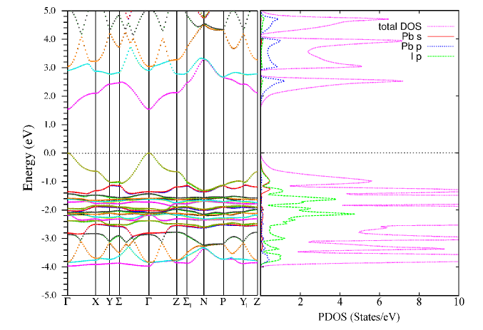
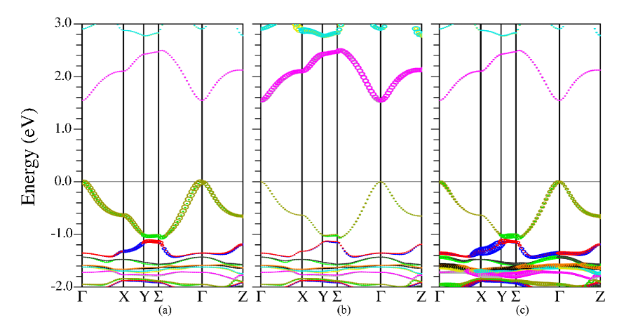
The density of states of MAPbI3 is shown in Fig. 2, where we see that the low-lying conduction bands are derived from Pb p states. On the other hand, the bands in the range -4 eV to -2 eV are dominated by iodine-derived states. The valence band just below the Fermi energy is derived from lead s and iodine p states. These observations become clear upon considering the atomic orbital character of the bands, which is presented in Fig. 3. The size of the circles is indicative of the contribution of the chosen atomic orbital to the eigenstates at each k-point. The CBM is derived mostly from Pb 6p states. The VBM, on the other hand, is a mixture of Pb 6s and I 5p states. The antibonding state formed from these s and p states is pushed up in energy close to the Fermi level. The large contribution of Pb 6s states to the VBM and Pb 6p states to the CBM suggests that there are strong optical transitions between the VBM and CBM , hence the usefulness of this material in solar applications.
CH3NH3PbBr3 (MAPbBr3) has a cubic unit cell. Its band structure is shown in Fig. 4, and, as expected, the band gap occurs at point R(1/2, 1/2, 1/2) in the Brillouin zone. As with the case of MAPbI3, its VBM is a mixture of Pb 6s and Br 4p states, whereas its CBM is derived from Pb 6p states. In the absence of SOC, its CBM is six-fold degenerate (including spin degeneracy). Due to SOC, its CBM is split into a doublet and a quartet . The doublet is lowered in energy by an amount , whereas the quartet is raised in energy by /, where eV. Similar perovskite structures, namely CsSnX3 (X=Cl, Br, I), where Sn replaces Pb, show a much smaller spin splitting of eV.39 Since the VBM is composed of Pb s and Br p orbitals, it is shifted slightly upward due to SOC on Br atoms. The large energy split of the CBM is, of course, due to the strong SOC on Pb atoms.

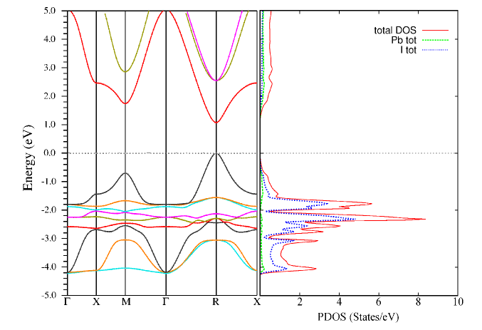
Finally, we consider the CsPbI3 crystal. At high temperature (634K), the crystal is cubic, but at room temperature, it is strongly distorted to an orthorhombic structure. Based on LDA and sx-LDA calculations, it has been suggested that, under hydrostatic pressure, the cubic phase might become a topological insulator.2 Calculations made using sx-LDA suggest a gap of 0.566 eV for CsPbI3 and 0.218 eV for CsSnI3. With decreasing lattice constants, the band width increases and the band gap decreases; at some critical pressure, band inversion occurs. For CsPbI3 and CsSnI3, those critical pressures are predicted to be 3.33 GPa and 0.96 GPa, respectively. However, GW calculations on CsSnI3 give a much larger band gap of 1.008 eV.39 Our calculation on the cubic phase of CsPbI3 shows that the band gap is 1.07 eV, larger by 0.5 eV than predicted by sx-LDA. Assuming linear dependence of the energy gap on lattice constant,2 a critical pressure of 6.6 GPa has to be applied to cause band inversion.
The band structure of cubic CsPbI3 is shown in Fig. 5. The band gap occurs at point R. As in the cases discussed previously, its CBM is derived from Pb 6p states, whereas its VBM is a mixture of Pb 6s and I 5p states. Without SOC, the calculated band gap is 2.27 eV, and the CBM is six-fold degenerate (including spin degeneracy). SOC on Pb splits its CBM into a doublet and a quartet . The doublet is lowered in energy by 1.1 eV, while the quartet is raised by 0.55 eV. On the other hand, SOC on the I atoms raises the VBM by 0.1 eV.
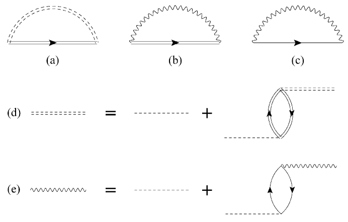
As a further check on our results for cubic CsPbI3, we repeated the calculation of the band gap using the GW approximation within the linear augmented plane wave formalism.40 In this method, the electron’s proper self energy * is approximated as a product of the electron Green’s function (G) and an effective interaction term (W). We carried out the calculation in the absence of spin-orbit coupling and using the G0W0 and GW0 approximations. The electron’s proper self energy in these approximations is shown graphically in Fig. 6. We found that within the G0W0 approximation, the band gap is 2.04 eV, and it increases to 2.19 eV upon employing the GW0 approximation. This result is in excellent agreement with, the value of 2.27 eV, which we obtained for the band gap, in the absence of SOC, by using the modified Becke-Johnson form of the exchange potential.
In conclusion, we have presented electronic structure calculations on six lead halide compounds using the modified Becke-Johnson method. We used the experimental crystal structure of these compounds at room temperature. We found that by modifying the parameters that characterize the TB-mBJ method, we obtain band gaps that are in excellent agreement with experiment. Using this new set of parameters, one should be able to predict the electronic structure of phases of these compounds that occur at different temperatures, as well as those of similar compounds obtained by replacing the alkali metal with various organic cations.
Acknowledgements.
We gratefully acknowledge support by NSF under grant No. HRD-0932421.References
- (1) Kojima, A.; Teshima, K.; Shirai, Y.; Miyasaka, T. Organometal Halide Perovskites as Visible-Light Sensitizers for Photovoltaic Cells. J. Am. Chem. Soc. 2009, 131, 6050–6051.
- (2) Jin, H.; Im, J.; Freeman, A. J. Topological Insulator Phase in Halide Perovskite Structures. Phys. Rev. B 2012, 86, 121102.
- (3) Yang, K.; Setyawan, W.; Wang, S.; Nardelli, M. B.; Curtarolo, S. A Search Model for Topological Insulators with High-Throughput Robustness Descriptors. Nature Materials 2012, 11, 614–619.
- (4) Etgar, L.; Gau, P.; Xue, Z.; Peng, Q.; Chandiran, A. K.; Liu, B.; Nazeeruddin, M. K.; Grätzel, M. Mesoscopic CH3NH3PbI3/TiO2 Heterojunction Solar Cells. J. Am. Chem. Soc 2012, 134, 17396–17399.
- (5) Ball, J. M.; Lee, M. M.; Hey, A.; Snaith, H. J. Low-Temperature Processed Meso-Superstructured to Thin-Film Perovskite Solar Cells. Energy Env. Sci. 2013, 6, 1739–1743.
- (6) Heo, H. J.; Im, S. H.; Noh, J. H.; Mandal, T. N.; Lim, C.-S.; Chang, J. A.; Lee, Y. H.; Kim, H.-j.; Sarkar, A.; Nazeeruddin, Md. K.; Grätzel, M.; Seok, S. I. Efficient Inorganic-Organic Hybrid Heterojunction Solar Cells Containing Perovskite Compound and Polymeric Hole Conductors. Nature Photonics 2013, 7, 486–491.
- (7) Kim, H.-S.; Lee, J.-W.; Yantara, N.; Biox, P. B.; Kulkarni, S. A.; Mhaisalker, S.; Grätzel, M.; Park, N.-G. High Efficiency Solid-State Sensitized Solar Cell-Based on Submicrometer Rutile TiO2 Nanorod and CH3NH3PbI3 Perovskite Sensitizer. Nanolett. 2013, 13, 2412–2417.
- (8) Bi, D.; Yang, L.; Boschloo, G.; Hagfeldt, A.; Johansson, E. M. J. Effect of Different Hole Transport Materials on Recombination in CH3NH3PbI3 Perovskite-Sensitized Mesoscopic Solar Cells. J. Phys. Chem. Lett. 2013, 4, 1532–1536.
- (9) Cai, B.; Xing, Y.; Yang, Z.; Zhang, W.-H.; Qiu, J. High Performance Hybrid Solar Cells Sensitized by Organolead Halide Perovskites. Energy Env. Sci. 2013, 6, 1480–1485.
- (10) Eperon, G. E.; Burlakov, V. M.; Docampo, P.; Goriely, A.; Snaith, H. J. Morphological Control for High Performance, Solution-Processed Planar Heterojunction Perovskite Solar Cells. Advanced Functional Materials 2014, 24, 151–157.
- (11) Laban, W. A.; Etgar, L. Depleted Hole Conductor-Free Lead Halide Iodide Heterojunction Solar Cells. Energy Env. Sci. 2014, 6, 3249–3253.
- (12) Stranks, S. D.; Eperon, G. E.; Grancini, G.; Menelaou, C.; Alcocer, M. J. P.; Leijtens, T.; Herz, L. M.; Petrozza, A.; Snaith, H. J. Electron-Hole Diffusion Lengths Exceeding 1 Micrometer in an Organometal Trihalide Perovskite Absorber. Science 2013, 342, 341–344.
- (13) Mosconi, E.; Amat, A.; Nazeeruddin, Md. K.; Grätzel, M.; De Angelis, F. First-Principles Modeling of Mixed Halide Organometal Perovskites for Photovoltaic Applications. J. Phys. Chem. C 2013, 117, 13902–13913.
- (14) Wang, Y.; Gould, T.; Dobson, J. F.; Zhang, H.; Yang, H.; Yao, X.; Zhao, H. Density Functional Theory Analysis of Structural and Electronic Properties of Orthorhombic Perovskite CH3NH3PbI3. Phys. Chem. Chemical Phys. 2014, 16, 1424–1429.
- (15) Umari, P.; Mosconi, E.; De Angelis, F. Relativistic GW calculations on CH3NH3PbI3 and CH3NH3SnI3 Perovskites for Solar Cell Applications. Scientific Reports 2014, 4, Article number: 4467.
- (16) Lee, M. M.; Teuscher, J.; Miyasaka, T.; Murakami, T. N.; Snaith, H. J. Efficient Hybrid Solar Cells Based on Meso-Superstructured Organometal Halide Perovskites. Science 2012, 338, 643–647.
- (17) Noh, J. H.; Im, S. H.; Heo, J. H.; Mandal, T. N.; Seok, S. I. Chemical Management for Colorful, Efficient, and Stable Inorganic-Organic Hybrid Nanostructured Solar Cells. Nano Lett. 2013, 13, 1764–1769.
- (18) Burschka, J.; Pellet, N.; Moon, S.-J.; Humphry-Baker, R.; Gao, P.; Nazeeruddin, M. K.; Grätzel, M. Sequential Deposition as a Route to High-Performance Perovskite-Sensitized Solar Cells. Nature 2013, 499, 316–319.
- (19) Liu, M.; Johnston, M. B.; Snaith, H. J. Efficient Planar Heterojunction Perovskite Solar Cells by Vapour Deposition. Nature 2013, 501, 395–398.
- (20) Kohn, W.; Sham, L. J. Self-Consistent Equations Including Exchange and Correlation Effects. Phys. Rev. 1965, 140, A1133–A1138.
- (21) Perdew, J. P.; Burke, K.; Ernzerhof, M. Generalized Gradient Approximation Made Simple. Phys. Rev. Lett. 1996, 77, 3865–3868.
- (22) Becke, A. D. A New Mixing of Hartree-Fock and Local Density-Functional Theories. J. Chem Phys. 1993, 98, 1372–1377.
- (23) Bechstedt, F.; Fuchs, F.; Kresse, G. Ab-initio Theory of Semiconductor Band Structures: New Developments and Progress. Phys. Status Solidi B 2009, 246, 1877–1892.
- (24) Becke, A. D.; Johnson, E. R. A Simple Effective Potential for Exchange. J. Chem. Phys. 2006, 124, 221101.
- (25) Tran, F.; Blaha, P.; Schwarz, K. Band Gap Calculations with Becke-Johnson Exchange Potential. J. Phys.: Condens. Matter 2007, 19, 196208.
- (26) Tran; F.; Blaha, P. Accurate Band Gaps of Semiconductors and Insulators with a Semilocal Exchange-Correlation Potential. Phys. Rev. Lett. 2009, 102, 226401.
- (27) Becke, A. D.; Roussel, M. R. Exchange Holes in Inhomogeneous Systems: A Coordinate-Space Model. Phys. Rev. A 1989, 39, 3761–3767.
- (28) Koller, D.; Tran; F.; Blaha, P. Merits and Limits of the Modified Becke-Johnson Exchange Potential. Phys. Rev. B 2011, 83, 195134.
- (29) Koller, D.; Tran, F.; Blaha, P. Improving the Modified Becke-Johnson Exchange Potential. Phys. Rev. B 2012, 85, 155109.
- (30) Blaha, P.; Schwarz, K.; Madsen, G. K. H.; Kvasnicka, D.; Luitz, J. WIEN2K: An Augmented Plane Wave and Local Orbitals Program for Calculating Crystal Properties, edited by Schwarz, K. Techn. Vienna University of Technology, Austria), 2001.
- (31) Poglitsch, A.; Weber, D. Dynamic Disorder in Methylammoniumtrihalogenoplumbates (II) Observed by Millimeter-Wave Spectroscopy. J. Chem. Phys 1987, 87, 6373–6378.
- (32) Mashiyama, H.; Kurihara, Y.; Azetsu, T. Disordered Cubic Perovskite Structure of CH3NH3PbX3 (X=Cl,Br,I). J. Korean Physical Soc. 1998, 32, S156–S158.
- (33) Moreira, R. L.; Dias, A. Comment on “Prediction of Lattice Constant in Cubic Perovskites”. J. Phys. Chem. Solids 2007, 68, 1617–1622.
- (34) Stoumpos, C. C.; Malliakas, C. D.; Peters, J. A.; Liu, Z.; Sebastian, M.; Im, J.; Chasapis, T. C.; Wibowo, A. C.; Chung, D. Y.; Freeman, A. J.; Wessels, B. W.; Kanatzidis, M. G. Crystal Growth of the Perovskite Semiconductor CsPbBr3: A New Material for High-Energy Radiation Detection. Cryst. Growth Des. 2013, 13, 2722–2727.
- (35) Trots, D. M.; Myagkota, S. V. High-Temperature Structural Evolution of Caesium and Rubidium Triiodoplumbates. J. Phys. Chem. Solids 2008, 69, 2520–2526.
- (36) Baikie, T.; Fang, Y.; Kadro, J. M.; Schreyer, M.; Wei, F.; Mhaisalkar, S. G.; Graetzel, M.; White, T. J. Synthesis and Crystal Chemistry of the Hybrid Perovskite (CH3NH3)PbI3 for Solid-State Sensitised Solar Cell Applications. J. Mater. Chem. A 2013, 1, 5628–5641.
- (37) Liu, Z.; Peters, J. A.; Stoumpos, C. C.; Sebastian, M.; Wessels, B. W.; Im, J.; Freeman, A. J.; Kanatzidis, M. G. Heavy Metal Ternary Halides for Room-Temperature X-Ray and Gamma-Ray Detection. Proc. SPIE 2013, 8852, 88520A.
- (38) Yunakova, O. N.; Miloslavskii, V. K.; Kovalenko, E. N. Exciton Absorption Spectrum of Thin (KI)1-x(PbI2)x films. Functional Materials 2013, 20, 59–63.
- (39) Huang, L. Y.; Lambrecht, W. R. L. Electronic Band Structure, Phonons, and Exciton Binding Energies of Halide Perovskites CsSnCl3, CsSnBr3, and CsSnI3. Phys. Rev. B 2013, 88, 165203.
- (40) Jiang, H.; Gómez-Abal, R. I.; Li, X.-Z.; Meisenbichler, C.; Ambrosch-Draxl, C.; Scheffler, M. FHI-gap : A GW Code Based on the All-Electron Augmented Plane Wave method. Computer Phys. Commun. 2013, 184, 348–366.