Organic Magnetoelectroluminescence for Room Temperature Transduction between Magnetic and Optical Information
Abstract
Magnetic and spin-based technologies for data storage and processing pose unique challenges for information transduction to light because of magnetic metals’ optical loss, and the inefficiency and resistivity of semiconductor spin-based emitters at room temperatureAwschalom and Flatte (2007). Transduction between magnetic and optical information in typical organic semiconductors poses additional challenges as the Faraday and Kerr magnetooptical effects rely on the electronic spin-orbit interactionMeier and Zachachrenya (1984), and the spin-orbit interaction in organics is weakNaber et al. (2007); Vardeny (2010). Other methods of coupling light and spin have emerged in organics, however, as the spin-dependent character of exciton recombination, with spin injection from magnetic electrodes, provides magnetization-sensitive light emissionDediu et al. (2002); Davis and Bussmann (2003), although such approaches have been limited to low temperature and low polarization efficiencyNguyen et al. (2012). Here we demonstrate room temperature information transduction between a magnet and an organic light emitting diode that does not require electrical current, based on control via the magnet’s remanent field of the exciton recombination process in the organic semiconductor.
Organic semiconductor devices have become a ubiquitous lighting technology due to their flexibility, inexpensive character, and highly efficient light output. Organic information processing also has an important niche where computational speed is less important than flexibility or expense. Nonvolatile information storage in organic electronics poses a challenge, as organic semiconductor flash memory currently have high leakage currents due to the large electric fields required to change transport properties in organic semiconductorsSekitani et al. (2009). The non-volatility, speed, and low energy consumption of magnetic memory make it fundamentally attractive for integration with organics although magnetic metals have large impedence mismatches with organics. This can be overcome using coupling through a magnet’s fringe field at zero applied field (remanent field) as demonstrated in organic electronic devicesWang et al. (2012a); Macià et al. (2013); Harmon et al. (2013). Efficient coupling via the magnet’s remanent field between light emission in organic devices and a magnetic memory would broaden the range of applicability of flexible, inexpensive organic electronics. Our demonstration of efficient room-temperature coupling between an organic light-emitting diode and a few-nanometer-thick magnetic film can be explained quantitatively within a theory of spin-dependent exciton recombination in the organic semiconductor, influenced only by the remanent fringe fields of the magnetic material.
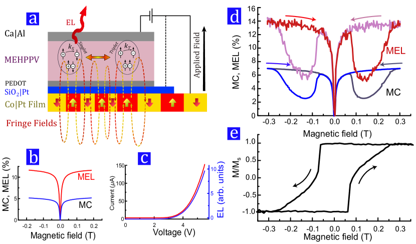
Organic semiconductor sandwich devices, used for example in organic light-emitting diodes (OLEDs), consist of a thin film of an organic semiconductor (or several layers thereof) sandwiched between a bottom and top electrode. The organic semiconductor is typically intrinsic, and is essentially void of charge carriers. Therefore one of the electrodes is chosen to efficiently inject electrons, and the other to efficiently inject holes. For this purpose low and high-work function metals, respectively, are chosen. Recombination of electron-hole pairs leads to electroluminescence, as shown in Fig. 1a. Transport of the injected carriers through the organic film occurs via a sequence of hops along a path connecting the top electrode to the bottom electrode, and the rate of transport and/or recombination is dramatically affected by variations in the local magnetic field along the path, as found in numerous experimental and theoretical studies Kalinowski et al. (2003); Francis et al. (2004); Prigodin et al. (2006); Bobbert et al. (2007); Desai et al. (2007); Hu and Wu (2007). In the transport regime, this effect is known as organic magnetoresistance (OMAR), and the corresponding effect in the electroluminescent output we will denote as organic magnetoelectroluminescence (OMEL). Typically the source of that inhomogeneous field is the nuclear hyperfine field, which is random and spatially uncorrelated. The origin of OMAR can be traced back to interactions between paramagnetic charge pairs that occur at bottle-neck sites (sites that crucially affect the transport and/or electroluminescent properties). These interactions are often spin-selective, and the reaction rate depends on the angle between the local spin-quantization axis (provided by the local magnetic field) for the two paramagnetic species. An applied magnetic field exceeding the hyperfine field strength forces this angle to be close to zero everywhere in the film, which shows up as magnetoconductance (MC) and/or magnetoelectroluminescence (MEL) with typical features like those in Fig. 1b.
Large gradients in the magnitude of the random local field can lead to fringe-field-driven MC and MEL, and devices were constructed that utilize fringe fields from an unsaturated magnetic film to supply such gradients Wang et al. (2012a); Macià et al. (2013); Harmon et al. (2013). This paper will primarily discuss such fringe-field effects, but “ordinary” OMAR and OMEL (based on, e.g., hyperfine fields) is also investigated as a reference. The exact nature of the paramagnetic pairs remains hotly debated, and the possibilities include electron-hole pair recombination to form singlet or triplet excitons Prigodin et al. (2006), or recombination to form singlet bipolarons Bobbert et al. (2007), and collision reactions between electrons or holes with long lived triplet excitons Desai et al. (2007). As the fringe-field MEL mechanism is driven by fringe-field gradients, independent of the mechanism of ordinary OMAR and OMEL, the effects presented here should be found in organic materials independent of the mechanism of OMAR and OMEL, including in materials where there is no OMAR and OMELHarmon et al. (2013).
As shown in Fig. 1a our devices are OMAR/OLED devices fabricated on top of a ferromagnetic thin film. The device fabrication starts with the metal deposition of a ferromagnetic multilayered thin film made of Cobalt (Co) and Platinum (Pt). Those films have perpendicular magnetic anisotropy; the spins tend to align in the direction orthogonal to the film plane. In presence of a large magnetic field out of the film plane the CoPt films are uniformly magnetized with all the spins pointing opposite to the direction of the applied field. At lower fields the films form magnetic domains—some regions with spins pointing up and others with spins pointing down—to lower the magnetostatic energy. These magnetic domains create strong varying fringe fields close to the surface of the CoPt films, which penetrate the OMAR/OLED device. In order to electrically insulate the OMAR/OLED device from the ferromagnetic film we deposit a thin dielectric followed by a conductive nonmagnetic layer on top of the magnetic film. These electrically insulated magnetic films prove that fringe fields—and not electrical currents—are responsible for the coupling between the ferromagnetic layer and the OMAR/OLED device. However, the strength and spatial correlation length of magnetic fringe fields depend sensitively on the distance from the magnetic film to the organic film. The insulating layer increases this distance reducing the effect. As a result we report results primarily on devices without this layer, which show the largest effects, and study devices with insulating layers to rule out spin injection and tunneling anisotropic magnetoresistive devices.
A conducting polymer layer (20 nm) of poly(3,4-ethylenedioxythiophene) poly(styrenesulfonate) (PEDOT:PSS, referred to as simply PEDOT from now on) was spin-coated from water suspension and serves as the hole-injecting layer. PEDOT is commonly employed for this purpose in organic light-emitting diode devices.Kim et al. (2002) We chose poly[2-methoxy-5-(2-ethylhexyloxy)-1,4-phenylenevinylene] (MEHPPV) as the luminescent polymer, as it is widely used as a red emitter in OLEDsMalliaras et al. (1998). The MEHPPV layer (55 nm) was deposited by spin-coating from toluene solution. Finally, Calcium (Ca) (6 nm, serving as the electron-injecting top contact) covered by Aluminum (Al) (12 nm) was deposited by vacuum evaporation through a shadow mask. The active device area is roughly 1 mm2. The Al capping layer is required to protect the highly reactive Ca layer. The contributions of the PEDOT and Ca electrodes to the device resistance (and magnetoresistance) are negligible, since they are metals, whereas MEHPPV is an intrinsic semiconductor. The EL is measured through the semitransparent top electrode, and recorded by a photomultiplier tube. All measurements reported here are at room temperature.
Figure 1b shows a typical MC and MEL trace, and Fig. 1c the IV and EL curves, for an organic device without a magnetic film and whose MC/MEL is therefore caused by the random hyperfine fields, as described above. This device will serve us as a reference when, later on, we will discuss fringe-field induced MC/MEL. It is seen that the hyperfine induced MC and MEL responses have a magnitude of 5 % and 10 %, respectively, in our MEHPPV devices. The effects essentially saturate for applied fields in excess of 0.1 T, are non-hysteretic, and have a full-width-at-half-maximum of approximately 20 mT. The effects are also independent of the direction of the applied magnetic field, and nearly independent of the MEHPPV layer thickness. In the present work, we have chosen to work with a thin MEHPPV layer (55nm) such that the distance from the ferromagnetic film does not vary much between different locations in the MEHPPV film.
Now we turn our attention to the MC/MEL responses of the fringe-field OMAR devices, and the correlation between these effects and the film magnetization, . Figure 1d shows the measured MC and MEL curves, and e shows the magnetization loop measured by magneto-optic Kerr effect (MOKE) (see methods section). In these measurements, the magnetic field is applied perpendicularly to the device plane, and is swept smoothly from large negative to large positive fields (black lines) and back (red lines). It is seen that the magnetization response is hysteretic, and that assumes its saturation value for fields larger than approximately 0.25 T in magnitude. is unsaturated between roughly and T. The MC/MEL curves outside the unsaturated magnetization regime clearly mirror the data in non-magnetic devices (panel b), and are explained by the “normal” hyperfine OMAR effect. In the unsaturated region, the data curves develop characteristic “ears”. These are the signature of fringe-field effects. We have previously given a detailed experimental and theoretical characterization of the transport aspect of this effect.Wang et al. (2012a); Macià et al. (2013); Harmon et al. (2013) In the present work, we demonstrate for the first time that fringe-field effects lead to a sizable room-temperature MEL response, of up to 6% at room temperature for the present device. This can be comparable to MEL effects that occur only at low temperature, such as those recently reported in spin-valvesNguyen et al. (2012) and high-magnetic-field effects for OLEDsWang et al. (2012b).
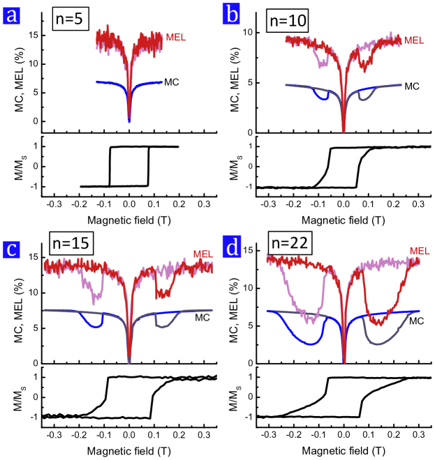
Next we examine the relation between the magnetic film’s response characteristics and MC/MEL by fabricating OMAR/OLED devices on several different ferromagnetic electrodes. In this work, the different magnetic responses are studied by fabricating ferromagnetic films consisting of Cobalt (Co) and Platinum (Pt) multilayers with a different number of repeats, . We studied devices with , and 30 (film thicknesses varied from 4 nm to 24 nm). The magnetization in the ferromagnetic films reverses through nucleation, growth, and annihilation of magnetic domains. When the magnetic films are saturated (all spins pointing towards the same direction) there are no magnetic fringe fields on top. When the magnetic films are unsaturated the strength of the magnetic fringe fields created by magnetic domains increases (almost linearly) with the thickness of the ferromagnetic layer (i.e., with the number of repeats). Properties of CoPt ferromagnetic films have been characterized in detail (see Refs. Wang et al., 2012a and Macià et al., 2013). The data of Fig. 2 shows that the hysteretic magnetoresistance of the organic layer is directly correlated with the hysteretic magnetization of the ferromagnetic film. The fringe-field “ears” occur only in the unsaturated regime, where film’s magnetization breaks into domains with fringe fields occurring near the domain boundaries.
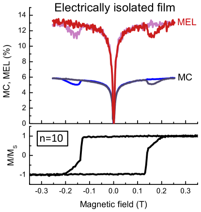
Figure 3 shows data similar to that reported in Fig. 2, but now for a device with an additional SiO2 layer inserted between the magnetic film and the OMAR/OLED device. This data exhibits all the same characteristics of the data without the insulating layer, and proves that the coupling between the magnetic film and the organic device is magnetic rather than electrical in nature. In particular this excludes mechanisms such as tunneling anisotropic magnetoresistance and spin-injection effects as the origin of the observed effects. The “ears” are however significantly smaller in magnitude. However, this was to be expected, since the insulating layer leads to a significantly larger separation between magnetic film and OMAR/OLED device as the overall spacer layer thickness increases from 20 nm to 45 nm with the layer inserted. We have previously examinedMacià et al. (2013) the dependence of the magnitude of the fringe-field magnetoresistance on the spacer layer thickness.
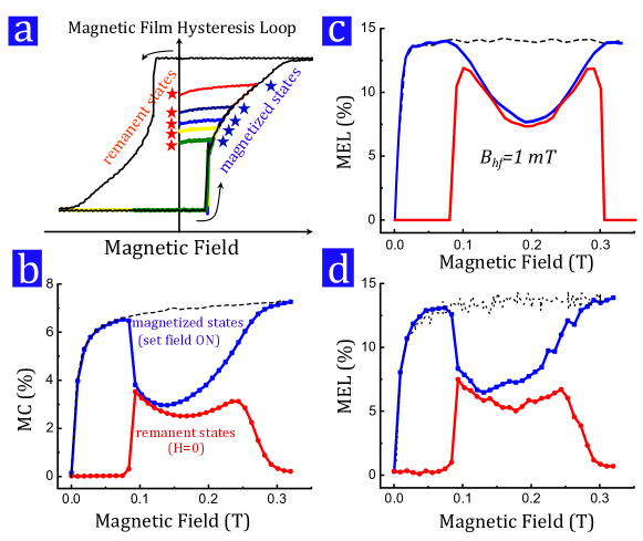
Magnetic domains can be present at zero applied field in our magnetic films. Such remanent states are prepared by applying a perpendicular field close to the film’s coercive field and then removing it (see Fig. 4a). Magnetization measurements and imaging prove that remanent domain states relax only slightly upon removal of the field. Therefore, we have access to remanent magnetization states ranging from negative to positive saturation. At zero applied field we observed how remanent fringe fields increase the conductance of the organic layer MEHPPV, suppressing OMAR. The same effect with a smaller strength was observed in the organic semiconductor Alq3Macià et al. (2013). Figure 4bd shows MC and MEL of a 55 nm thick MEHPPV film on top of a magnetic layer both in presence of and at zero magnetic field. The blue line depicts the measured values in presence of magnetic field whereas the red lines trace the values measured after removing the applied field (a sketch of the measuring sequence is shown in Fig. 4a): We first saturated the sample with a large negative field, then we set a positive field value from 0 to 0.3 T and measured the conductivity of the organic layer (blue points), and then we removed the applied field and again measured the organic’s conductivity (red points). Here we show that the electroluminiscence increases up to 6 for remanent magnetic domain states of the ferromagnetic layer. In contrast to fringe fields from the same domain configuration in an applied magnetic field (near the coercive field) the MEL increases rather than decreases.
We now examine whether the large fringe-field effects observed in the MEL can be explained by theory. We consider a two-site model where an electron and hole (a polaron pair) occupy two nearby sites. The spin configuration of the polaron pair undergoes transitions due to the different magnetic interactions present; in our case these interactions consist of
| (1) |
which are the applied, hyperfine, and fringe-field Hamiltonians respectively. The polaron pairs recombine into excitons at different rates, and , depending on the pair’s spin since the singlet and triplet states have different energies and wavefunctionsKersten et al. (2011) (see. schematic Fig. 1a); alternatively the pair could disassociate at a rate . Once an exciton is formed, the large exchange energy precludes any further spin evolution. In the absence of large spin-orbit interactions, spin selection rules dictate that exciton recombination (i.e. photon emission) occurs only from the singlet exciton state. Assuming that radiative recombination is the only viable pathway for a newly formed singlet exciton, each singlet exciton will produce a single photon such that MEL can be defined in terms of , the singlet fraction of excitons: .
To calculate the MEL we employ the stochastic Liouville equation for the polaron pair spin density matrix, :Kubo (1963); Haberkorn (1976)
| (2) |
where and are the singlet and triplet projection operators. The steady-state singlet and triplet exciton fractions areJones and Hore (2010)
| (3) |
where runs over and . All rates (times) are in units of the hyperfine field frequency (period), () where is the width of the Gaussian distribution of hyperfine fields. For simplicity we assume and .
To proceed with the calculation, one must have knowledge of the fringe fields present in the organic layer. In our previous analysisHarmon et al. (2013) on fringe-field induced magneto-resistance, elementary magnetostatics were used to calculate fringe fields from XMCD images of the magnetic domains. The samples described herein have the same composition. We use therefore the statistical analysis from the aforementioned XMCD images to model the fringe-field distributions. Given the fact that fringe fields vanish at magnetic saturation and are largest and most varying at , we model the fringe-field distribution as normal distribution with mean zero and a field dependent standard deviation. Each component of the fringe-field gradient, is modeled likewise. The field dependent standard deviations follow a parabola defined in the upper half-plane according to
| (4) |
| (5) |
where is the field at which the magnet starts developing domains (obtainable from either the MOKE data or the MEL measurements) and is the field corresponding roughly to . and mark the parabola’s vertex and are the only free parameters. However, from analysis of samples of the same composition on which XMCD images have been acquired, their values are roughly 40 mT and 1 mT/nm respectively for a spacer width of 20 nm.
The results of this theory and model are shown in Fig. 4c. The and are chosen from Figure 1e. The values of (=) and (=) are chosen to achieve a saturated MEL percentage near that of Figure 1d (). The values for the hopping rates fall into the intermediate hopping regime () which is necessary to have any fringe-field effect.
Remanent fringe fields generated from the domain structure of the magnetic film cause the observed dramatic modification of the electroluminescence from an organic light emitting diode at room temperature. As a uniform, perpendicularly magnetized film produces no remanent fields, the source of these fringe fields is the regions where the magnetization changes most rapidly, corresponding to domain walls. The faster the magnetization changes, or the smaller the domain size, the larger the remanent fields. Thus this approach of interfacing magnetic information encoded in the domain structure with an organic light emitting diode should become more effective and efficient as the magnetic domain sizes shrink. We note as well that the MEL is significantly larger than the MC, indicating that (for MEHPPV) fringe-field optical coupling and readout will have greater sensitivity than fringe-field electrical coupling and readout of magnetic information.
I Methods
I.1 Fringe-field device fabrication
The organic semiconductor semi-spin valve consists of a ferromagnetic layer, a hole-injecting layer, an organic semiconductor, and a top electrode. The ferromagnetic electrode is a CoPt multilayer with the number of repeats varied from 4 to 22 deposited using electron-beam evaporation in ultra high vacuum on oxidized Si wafers for device studies and Si supported Si3N4 membranes for magnetic domain imaging studies using an x-ray transmission microscope. Optical lithography is used to define lines in the ferromagnetic thin film. A hole-injecting layer, conducting polymer poly(3,4-ethylenedioxythiophene) poly(styrenesulfonate) (PEDOT:PSS), was deposited by spin-coating from an aqueous suspension (suspension purchased from H. C. Starck, CLEVIO P VP AI 4083). A 55 nm thick film of organic semiconductor MEHPPV (purchased from American Dye Source, Inc.) was deposited by spin coating with 3mg/ml solution in Toluene. The electron injecting layer, Ca (6 nm) covered by Al (12 nm) was deposited by thermal evaporation at room temperature through a metal stencil to obtain a cross point device geometry. The ferromagnetic electrodes were characterized by magnetic force microscopy (MFM), ferromagnetic resonance (FMR), vibrating sample magnetometery (VSM), and magneto-optical Kerr effect (MOKE).
I.2 Measurements
Magnetoresistance measurements were done in a closed-cycle He cryostat positioned between the poles of an electromagnet. The measurements reported here are all at room-temperature. Magnetoresistance (MR) measurements were performed using a Keithley 2400 sourcemeter. Electroluminescence was measured by photomultiplier tube through the top electrode Ca/Al. X-ray measurements were performed at the Advanced Light Source (ALS) at the Lawrence Berkeley National Laboratory. Images were taken with XM-1 zone-plate microscope at beamline 6.1.2.
II Acknowledgements
This work was supported by ARO MURI Grant No. W911NF-08-1-0317. FM thanks support from EU, MC-IOF 253214.
References
- Awschalom and Flatte (2007) D. D. Awschalom and M. E. Flatte, Nature Physics 3, 153 (2007).
- Meier and Zachachrenya (1984) F. Meier and B. P. Zachachrenya, Optical Orientation: Modern Problems in Condensed Matter Science, vol. 8 (North-Holland, Amsterdam, 1984).
- Naber et al. (2007) W. J. M. Naber, S. Faez, and W. G. van der Wiel, J. Phys. D-Appl. Phys. 40, R205 (2007).
- Vardeny (2010) Z. V. Vardeny, ed., Organic Spintronics (CRC Press, Heidelberg, 2010).
- Dediu et al. (2002) V. Dediu, M. Murgia, F. C. Matacotta, C. Taliani, and S. Barbanera, Solid State Communications 122, 181 (2002).
- Davis and Bussmann (2003) A. H. Davis and K. Bussmann, Journal of Applied Physics 93, 7358 (2003).
- Nguyen et al. (2012) T. D. Nguyen, E. Ehrenfreund, and Z. V. Vardeny, Science 337, 204 (2012).
- Sekitani et al. (2009) T. Sekitani, T. Yokota, U. Zschieschang, H. Klauk, S. Bauer, K. Takeuchi, M. Takamiya, T. Sakurai, and T. Someya, Science 326, 1516 (2009).
- Wang et al. (2012a) F. Wang, F. Macià, M. Wohlgenannt, A. D. Kent, and M. E. Flatté, Phys. Rev. X 2, 021013 (2012a).
- Macià et al. (2013) F. Macià, F. Wang, N. J. Harmon, M. Wohlgenannt, A. D. Kent, and M. E. Flatté, Appl. Phys. Lett. 102, 042408 (2013).
- Harmon et al. (2013) N. J. Harmon, F. Macià, F. Wang, M. Wohlgenannt, A. D. Kent, and M. E. Flatté, Phys. Rev. B 87, 121203(R) (2013).
- Kalinowski et al. (2003) J. Kalinowski, M. Cocchi, D. Virgili, P. Di Marco, and V. Fattori, Chem. Phys. Lett. 380, 710 (2003).
- Francis et al. (2004) T. L. Francis, O. Mermer, G. Veeraraghavan, and M. Wohlgenannt, New Journal of Physics 6, 185 (2004).
- Prigodin et al. (2006) V. N. Prigodin, J. D. Bergeson, D. M. Lincoln, and A. J. Epstein, Synth. Met. 156, 757 (2006).
- Bobbert et al. (2007) P. A. Bobbert, T. D. Nguyen, F. W. A. van Oost, B. Koopmans, and M. Wohlgenannt, Phys. Rev. Lett. 99, 216801 (2007).
- Desai et al. (2007) P. Desai, P. Shakya, T. Kreouzis, W. P. Gillin, N. A. Morley, and M. R. J. Gibbs, Phys. Rev. B 75, 094423 (2007).
- Hu and Wu (2007) B. Hu and Y. Wu, Nat. Mater. 6, 985 (2007).
- Kim et al. (2002) W. H. Kim, A. J. Makinen, N. Nikolov, R. Shashidhar, H. Kim, and Z. H. Kafafi, Appl. Phys. Lett. 80, 3844 (2002).
- Malliaras et al. (1998) G. G. Malliaras, J. R. Salem, P. J. Brock, and C. Scott, Phys. Rev. B 58, R13411 (1998).
- Wang et al. (2012b) J. Wang, A. Chepelianskii, F. Gao, and N. C. Greenham, Nat. Commun. 3, 1191 (2012b).
- Kersten et al. (2011) S. P. Kersten, S. A. J., B. Koopmans, and P. A. Bobbert, Phys. Phys. Lett. 106, 197402 (2011).
- Kubo (1963) R. Kubo, J. Math. Phys. 4, 174 (1963).
- Haberkorn (1976) R. Haberkorn, Mol. Phys. 32, 1491 (1976).
- Jones and Hore (2010) J. A. Jones and P. J. Hore, Chem. Phys. Lett. 488, 90 (2010).


