pagecommand=
A Silicon Nanocrystal Tunnel Field Effect Transistor
Abstract
In this work, we demonstrate a silicon nanocrystal Field Effect Transistor (ncFET). Its operation is similar to that of a Tunnelling Field Effect Transistor (TFET) with two barriers in series. The tunnelling barriers are fabricated in very thin silicon dioxyde and the channel in intrinsic polycrystalline silicon. The absence of doping eliminates the problem of achieving sharp doping profiles at the junctions, which has proven a challenge for large-scale integration and in principle allows scaling down the atomic level. The demonstrated ncFET features a on/off current ratio at room temperature, a low leakage current at a bias, an on-state current on a par with typical all-Si TFETs and bipolar operation with high symmetry. Quantum dot transport spectroscopy is used to assess the band structure and energy levels of the silicon island.
The Complementary Metal–Oxide–Semiconductor (CMOS) technology is at the heart of modern electronic devices Sze and Ng (2007). The performance of its fundamental component, the Metal–Oxide–Semiconductor Field Effect Transistor (MOSFET), can be evaluated in terms of on/off output current ratio, off-state leakage current, and subthreshold slope Ferain, Colinge, and Colinge (2011). However, certain performance characteristics of the MOSFET are intrinsically limited by the physics involved in the device Sze and Ng (2007); Ferain, Colinge, and Colinge (2011); Ionescu and Riel (2011). For example, the thermal activation of carriers imposes a limit on the subthreshold slope, which cannot be inferior to Ferain, Colinge, and Colinge (2011). A promising approach is to take advantage of the exponential dependance of tunnelling current on the width of a barrier to block thermal electrons while enabling a fast transistor turn-on with gate voltage, as it is the case in tunnelling Field Effect Transistors (TFETs) Ionescu and Riel (2011) or Schottky barrier Field Effect Transistors Larson and Snyder (2006). In typical TFETs, a single tunnelling barrier is formed by doping the source, channel and drain to form a p–i–n-like junction Ionescu and Riel (2011). However, tight control of the doping profile is challenging because of dopant diffusion problems that prevent forming atomically sharp junctions Pierre et al. (2010), therefore limiting the built-in electric field and the on-state current Seabaugh and Zhang (2010).
In this work, we fabricated and characterized a transistor made out of an intrinsic silicon nanocrystal contacted by two metallic source/drain electrodes, which we call a nanocrystal Field Effect Transistor (ncFET, Fig. 1a).
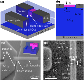
The switching mechanism relies on the gate-induced modulation of a tunnel barrier in a process very similar to a Schottky barrier FET Larson and Snyder (2006). This can, in principle, allow sub-60-mV/decade subthreshold slope and extremely low leakage current. Unlike many previous demonstrations of similar devices with self-assembled quantum dots Klein et al. (1997); Katsaros et al. (2010); Lachance-Quirion et al. (2014), ours is entirely nanofabricated with industry-compatible techniques. The ncFET also differs from Schottky barrier FETs with silicide source/drain Larson and Snyder (2006); Matheu (2012) by three facts. First, the leads are not made of a silicide but of an elemental metal. Second, the channel is very small in all spatial dimensions and separated from the leads by a thin insulator, which makes it effectively an island. Third, its very flexible fabrication process uses polycrystalline silicon (poly-Si) and differs wildly from planar Sze and Ng (2007) or silicon-on-insulator Ferain, Colinge, and Colinge (2011); Roche et al. (2012) MOSFETs. Doping is intentionally avoided to enable extreme scaling of the device dimensions and avoid the dopant diffusion and non-uniformity problems mentioned earlier.
The transistors were fabricated using a nanodamascene process based on the one of Dubuc et al. Dubuc, Beauvais, and Drouin (2008). An oxidized silicon substrate is patterned with electron beam lithography and a CF4/H2/He Inductively Coupled Plasma (ICP) process Guilmain et al. (2011) to produce wide and deep source/drain nanotrench and lateral gate trench. A 40-nm-thick amorphous silicon (a-Si) film is deposited using Low Pressure Chemical Vapor Deposition (LPCVD) at . An a-Si nanowire is then patterned over and perpendicular to the nanotrench using a C4F8/SF6 ICP etch Harvey-Collard et al. (2013). The resulting structure is shown in Fig. 1c. A Rapid Thermal Anneal (RTA) is used to form poly-Si with a thin film grain size in the range of to with the goal of forming an island with few or no grains. The tunnel junctions are prepared by etching the native oxide at the surface of the poly-Si nanowire using diluted hydrofluoric acid (HF) and letting it re-oxidize for 2 hours in cleanroom air before Ti deposition, which yields an estimated SiO2 thickness of . Titanium is deposited and then polished using a Chemical Mechanical Polishing (CMP) process Guilmain et al. (2013), which isolates the silicon island and yields the structure of Fig. 1d. This key step enables the unique nanocrystal geometry and positioning. Very interestingly, the nanodamascene poly-Si process opens the door to using different lead and channel materials, as well as integration over various types of substrates.
The transistor characteristics of the ncFET are shown in Fig. 2.
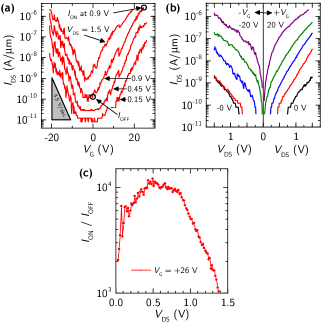
Current through all terminals is monitored to validate that source–drain current goes through the island and that gate leakage is always below and therefore negligible. The substrate is used as a back gate to supply voltage relative to the drain with an oxide thickness of . The lateral gate being located from the island in the featured device, its contribution is small compared with the back gate and hence is neglected in the following discussion. The channel width is .
As shown by the data of Fig. 2a, the transistor is a normally off device and works equally well for positive and negative gate biases. The current rises exponentially with gate bias, a clear sign of tunnelling. This rise shows no indication of saturation for all accessible gate biases. Since the source is a metal, supply of electrons should not be a limiting factor. Moreover, the junction being in principle close to atomically sharp, it can build much bigger electric fields than doped junctions Seabaugh and Zhang (2010). Therefore, better gate electrostatics (e.g. lower equivalent oxide thickness and source–gate overlap) are expected to yield significantly better Loh et al. (2010), while the demonstrated value of at and is already on a par with all-silicon TFETs that do not include CMOS technology boosters and source–gate overlap Loh et al. (2010); Ionescu and Riel (2011). The demonstrated and are both roughly two orders of magnitude smaller than Schottky barrier FETs Larson and Snyder (2006). Taking into account that could be further improved to (see discussion below), the ncFET then compares very favorably with both Schottky barrier FETs Larson and Snyder (2006) and optimized all-silicon TFETs Loh et al. (2010); Ionescu and Riel (2011).
A plateau of leakage current is observed at low and (Fig. 2a). Possible leakage mechanisms are thermionic emission over the barrierSeabaugh and Zhang (2010), Shockley-Read-Hall generationSeabaugh and Zhang (2010) at the lead–island interface, and direct or trap-assisted tunnelling through the island Seabaugh and Zhang (2010). Preliminary results at low temperature on similar devices indicate that the leakage plateau is mostly independent of temperature. Therefore, the most likely leakage mechanism is direct and potentially trap-assisted tunnelling. This would also be consistent with the high current noise and will be discussed again later. The leakage current is at . This is 40 times smaller than low operating power MOSFETs and 830 times smaller than high performance MOSFETs ITR (2011). The leakage current (extracted from Fig. 2a at ) reduces to at a lower value, which is the projected low-operating-power supply voltage ITR (2011).
An important parameter is the ratio. From the graph of Fig. 2c, it is seen that is maintained well above over a wide range of values, from to , and reaches . This makes the ncFET a very versatile device able to operate both at high and low supply voltage. While improving would require a longer channel or an improved processing, can be easily enhanced. In fact, redesigning the interconnect circuit could allow to push the gate swing to , improving to an extrapolated value of by increasing to , enough to start competing directly with the one of MOSFETs Ionescu and Riel (2011); ITR (2011). Such a high has already been achieved using a more favorable gate configuration Tsui and Lin (2004). Moreover, adding a state-of-the-art high-k dielectric gate stack could reduce the equivalent oxide thickness from to below . This would correspond to a scaling of the gate voltage from to and of the subthreshold slope from to below , making it useful for low-power applications.
We now investigate the similarity of the structure with quantum dots. This is motivated by the geometry of the device, which is expected to trap electrons inside the channel due to the thin oxide layer in the tunnel junction. In fact, quantum dot transport spectroscopy can provide us with insights on the band structure of the channel or island and help understand the transport mechanisms. In the quantum dot picture, the energy states of the electrons in the island are discrete due to the charging energy and quantum confinement energy Likharev (1999). The energy required to add an electron onto the island is then . A transport spectroscopy measurement can allow to identify these energy levels Hanson et al. (2007). It consists of a measurement of as a function of both and . The diamond-shaped regions of blocked current, called Coulomb diamonds, contain the information on the energy level structure of the island. Figure 3a shows such a measurement, where a wide, diamond-shaped region of blocked current appears in the center of the plot.

In our structure, the silicon gap appears as a large gap between the energy levels of the valence and conduction bands (Fig. 3f). If the temperature is higher than the small intraband levels, but much smaller than the gap, we then expect to see one large Coulomb diamond with an addition energy approximately equal to the silicon gap Sze and Ng (2007). Our data does agree with this model. From Fig. 3a (black dashed line), we extract an addition energy of , close but larger than the gap value. It is suspected that the difference could be accounted for by the very small dimension of the island in the vertical direction (around 5 to ), where quantum confinement causes an increase in bandgapMa et al. (2003). The high symmetry between positive and negative values of is a strong indication that the band alignment of Fig. 3f is experimentally correct. This allows us to describe qualitatively the band structure for different configurations of and . For example, the diagram of Fig. 3c illustrates the main leakage mechanism at high . When gate bias is applied (Fig. 3b or 3d), the bands are curved up or down, allowing to modulate the width of the tunnelling barrier. The electrostatic screening from the leads causes the gate to have more influence on the center of the channel than on its ends. This causes a band curvature like the one of Fig. 3e and 3g. Screening effects by the electrons in the channel are neglected, because they are expected to change only the quantitative behavior of the bands. In fact, in these bias configurations, the island is expected to form a potential well that would confine electrons or holes and produce Coulomb blockade at a lower temperature Prati et al. (2012). Indeed, the features observed at low of Fig. 3a (green dashed lines) could be attributed to poorly confined and/or temperature-blurred Coulomb blockade.
From the data of Fig. 2a and 3a, it is seen that the noise level is very high and sometimes telegraphic in nature (not shown). Moreover, charge jumps are visible in the diamond of Fig. 3a. It is suspected that the number of charge defects is large, producing charge fluctuators Zimmerman et al. (2007, 2008) or trap states that can affect the tunnel junctions. Because the tunnelling transport mechanism is extremely sensitive to distance, any small variation in the device’s electrostatic environment is transduced in large current fluctuations. It is unclear whether the defects are located in the surrounding dielectric, the SiO2 tunnel barrier or the island itself. Nevertheless, we do think that an anneal of the SiO2 tunnel junction would be beneficial. It should be added that it is expected that the titanium of the leads will consume part of the tunnel junction over time. This process can lead to traps in the barrier and time-evolving behavior. In the future, replacing the SiO2 and leads materials should be considered.
In summary, we have fabricated a tunnelling field effect transistor with metallic source and drain where the channel is made of a silicon nanocrystal. This transistor relies on intrinsic material for its operation, therefore eliminating the need for doping and allowing aggressive scaling down to the atomic level. Electronic transport is found to occur via tunnelling from the metal source to the channel conduction band at positive gate bias due to the strong electric field achieved in the absence of doping. A relatively good on/off current ratio, reaching , is demonstrated at room temperature over a wide range of source–drain bias. We argue that this could be improved to with better gate electrostatics. Quantum dot transport spectroscopy was used to assess the band structure and energy levels of the silicon island. It shows that the ncFET could potentially be used as a single electron transistor and trap single electrons or holes. Future investigations will address the details of the transport mechanisms through low temperature transport measurements.
The authors would like to thank S. Ecoffey for help with chemical mechanical polishing and J.-P. Richard for preliminary work on a-Si/poly-Si. This work was supported by NSERC, FRQNT, NanoQuébec, RQMP and CIFAR.
References
- Sze and Ng (2007) S. M. Sze and K. K. Ng, Physics of Semiconductor Devices, 3rd ed. (Wiley-Interscience, 2007).
- Ferain, Colinge, and Colinge (2011) I. Ferain, C. A. Colinge, and J.-P. Colinge, Nature 479, 310 (2011).
- Ionescu and Riel (2011) A. M. Ionescu and H. Riel, Nature 479, 329 (2011).
- Larson and Snyder (2006) J. Larson and J. P. Snyder, IEEE Transactions on Electron Devices 53, 1048 (2006).
- Pierre et al. (2010) M. Pierre, R. Wacquez, X. Jehl, M. Sanquer, M. Vinet, and O. Cueto, Nat Nano 5, 133 (2010).
- Seabaugh and Zhang (2010) A. C. Seabaugh and Q. Zhang, Proceedings of the IEEE 98, 2095 (2010).
- Klein et al. (1997) D. L. Klein, R. Roth, A. K. L. Lim, A. P. Alivisatos, and P. L. McEuen, Nature 389, 699 (1997).
- Katsaros et al. (2010) G. Katsaros, P. Spathis, M. Stoffel, F. Fournel, M. Mongillo, V. Bouchiat, F. Lefloch, A. Rastelli, O. G. Schmidt, and S. De Franceschi, Nat Nano 5, 458 (2010).
- Lachance-Quirion et al. (2014) D. Lachance-Quirion, S. Tremblay, S. A. Lamarre, V. Méthot, D. Gingras, J. Camirand Lemyre, M. Pioro-Ladrière, and C. N. Allen, Nano Letters 14, 882 (2014).
- Matheu (2012) P. Matheu, Investigations of Tunneling for Field Effect Transistors, Ph.D. thesis, University of California at Berkeley (2012).
- Roche et al. (2012) B. Roche, B. Voisin, X. Jehl, R. Wacquez, M. Sanquer, M. Vinet, V. Deshpande, and B. Previtali, Applied Physics Letters 100, 032107 (2012).
- Dubuc, Beauvais, and Drouin (2008) C. Dubuc, J. Beauvais, and D. Drouin, IEEE Transactions on Nanotechnology 7, 68 (2008).
- Guilmain et al. (2011) M. Guilmain, A. Jaouad, S. Ecoffey, and D. Drouin, Proceedings of the 36th International Conference on Micro- and Nano-Engineering (MNE), Microelectronic Engineering 88, 2505 (2011).
- Harvey-Collard et al. (2013) P. Harvey-Collard, A. Jaouad, D. Drouin, and M. Pioro-Ladrière, Microelectronic Engineering 110, 408 (2013).
- Guilmain et al. (2013) M. Guilmain, T. Labbaye, F. Dellenbach, C. Nauenheim, D. Drouin, and S. Ecoffey, Nanotechnology 24, 245305 (2013).
- Loh et al. (2010) W.-Y. Loh, K. Jeon, C.-Y. Kang, J. Oh, P. Patel, C. Smith, J. Barnett, C. Park, T.-J. K. Liu, H.-H. Tseng, P. Majhi, R. Jammy, and C. Hu, in Proceedings of the European Solid-State Device Research Conference (ESSDERC 2010) (2010) pp. 162–165.
- ITR (2011) “International technology roadmap for semiconductors report 2011,” (International Technology Roadmap for Semiconductors, 2011) Chap. Process Integration, Devices, and Structures (PIDS).
- Tsui and Lin (2004) B.-Y. Tsui and C.-P. Lin, IEEE Electron Device Letters 25, 430 (2004).
- Likharev (1999) K. Likharev, Proceedings of the IEEE 87, 606 (1999).
- Hanson et al. (2007) R. Hanson, L. P. Kouwenhoven, J. R. Petta, S. Tarucha, and L. M. K. Vandersypen, Rev. Mod. Phys. 79, 1217 (2007).
- Ma et al. (2003) D. D. D. Ma, C. S. Lee, F. C. K. Au, S. Y. Tong, and S. T. Lee, Science 299, 1874 (2003).
- Prati et al. (2012) E. Prati, M. D. Michielis, M. Belli, S. Cocco, M. Fanciulli, D. Kotekar-Patil, M. Ruoff, D. P. Kern, D. A. Wharam, J. Verduijn, G. C. Tettamanzi, S. Rogge, B. Roche, R. Wacquez, X. Jehl, M. Vinet, and M. Sanquer, Nanotechnology 23, 215204 (2012).
- Zimmerman et al. (2007) N. M. Zimmerman, B. J. Simonds, A. Fujiwara, Y. Ono, Y. Takahashi, and H. Inokawa, Applied Physics Letters 90, 033507 (2007).
- Zimmerman et al. (2008) N. M. Zimmerman, W. H. Huber, B. Simonds, E. Hourdakis, A. Fujiwara, Y. Ono, Y. Takahashi, H. Inokawa, M. Furlan, and M. W. Keller, Journal of Applied Physics 104, 033710 (2008).