Effect of realistic metal electronic structure on the lower limit of contact resistivity of epitaxial metal-semiconductor contacts
Abstract
The effect of realistic metal electronic structure on the lower limit of resistivity in [100] oriented -Si is investigated using full band Density Functional Theory and Semi-Empirical Tight Binding (TB) calculations. Using simulation unit cells guided by the interface chemistry of epitaxial CoSi2 on [100] oriented Si observed experimentally, it is shown that the ’ideal metal’ assumption fails in some situations and consequently underestimates the lower limit of contact resistivity in -Si by at least an order of magnitude at high doping concentrations. The mismatch in transverse momentum space in the metal and the semiconductor, the so-called ’valley filtering effect’, is shown to be dependent on the interface chemistry simulated. The results emphasize the need for explicit inclusion of the metal atomic and electronic structure in the atomistic modeling of transport across metal-semiconductor contacts.
Metal-Semiconductor (M-S) specific contact resistivity () is a key metric in the performance of nano-scaled semiconductor device technology. For example, to meet scaling requirements, the International Technology Roadmap for Semiconductors (ITRS)itr (2011) has called for a value of -cm2 by 2023.
Much of the existing experimental and theoretical work on improving M-S contact resistivity is driven by semi-classical models of electronic transport through the M-S interface. These models use empirically derived quantities such as Schottky Barrier Height (SBH), width and doping concentrations (see, for instance, the Wentzel, Kramers, Brillouin (WKB)-based model of Yu Yu (1970)) and have a limited applicability. The WKB approximation, for instance, is valid only in the limit that the barrier potential varies slowly compared to the electron wavelength Griffiths (2013).
From an atomistic modeling standpoint, Maassen et al. Maassen et al. (2013) recently reported the lower limits of contact resistivity in Si using full band Tight Binding (TB) calculations. They report specific contact resistivities in the low -cm2 range at doping concentrations close to the solubility limit of P in Si ( 710) Trumbore (1960). Weber Weber (2013) and Park et al.Park et al. (2013) have performed Non-Equilibrium Greens Function (NEGF) transport calculations on the M-S interface system that incorporates metallic electronic structure in an effective-mass based approach. While these investigations provide important insights into the transport mechanism at M-S interfaces at a level that surpasses semi-classical approaches, they ignore a number of important effects that manifest themselves at M-S interfaces as device dimensions are scaled down.
For instance, it is not possible to capture complicated Fermi Surfaces of metal silicides such as NiSi, TiSi and CoSi2 accurately in an effective-mass based approach. At extremely high doping concentrations (in the high 1020 cm-3 range and above), upper valleys in Si begin to conduct, so that the use of a single-band effective mass for Si is no longer valid. It is also unclear from these investigations if the ’ideal metal’ approximation of a spherical Fermi Surface (FS) Weber (2013) with sufficient modes to supply all semiconducting modes Maassen et al. (2013) is realistic.
Gao et al. Gao and Guo (2012) have investigated the electronic structure of the metal silicide-silicon interface using ab-initio Density Functional Theory (DFT) based calculations. Due to explicit inclusion of the metal electronic structure in their work, a more realistic picture of the factors governing electronic transport at these interfaces emerges. Their work, however, does not explicitly quantify the effect of including realistic metal electronic structure on eventual contact resistivity or on its lower bound in Si. It is also unclear to what extent epitaxial interface chemistry affects electronic transmission through the interface.
In this letter, the effect of realistic metal electronic structure on the lower limit of contact resistivity in [100] oriented -Si is quantified using full band DFT and TB calculations. Using simulation unit cells guided by the interface chemistry of epitaxial CoSi2 on [100] oriented Si observed experimentally, it is shown that the ’ideal metal’ assumption fails in some situations and consequently underestimates the lower limit of contact resistivity in -Si by at least an order of magnitude at high doping concentrations. The mismatch in transverse momentum space in the metal and the semiconductor, the so-called ’valley filtering effect’ Gao and Guo (2012); Weber (2013), is shown to be sensitive to the interface chemistry simulated. Finally, the limits to the applicability of such an analysis are also discussed in detail.
The CoSi2-Si epitaxial interface system observed experimentally Tung, Schrey, and Yalisove (1989) is chosen as a representative M-S system in this letter. Bulk CoSi2 has a 3 atom FCC unit cell with a Co atom at (0,0,0) and Si atoms at (,,) and (,,), where the lattice parameter 5.365 at room temperature. The experimental growth of epitaxial CoSi2 on [100] oriented -Si at its room temperature lattice parameter of 5.43 results in two dominant [100] epitaxial orientations with a mean lattice mismatch of about 0.81% in CoSi2 in the plane transverse to the interface. These are - [100] oriented CoSi2 lattice matched to [100] oriented Si, where the substrate is bound by [010] and [001] crystal orientations and [011] and [0-11] orientations. This motivates the use of two distinct unit cell cross sections for the M-S interface system. These unit cell cross sections are shown in Fig 1.
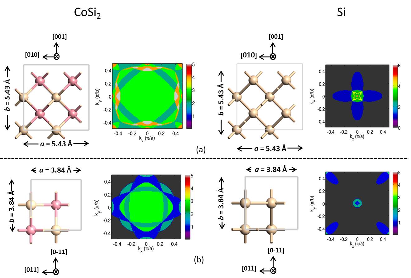
Using these unit cells as the starting point, the transverse-momentum resolved transmission spectra in [100] oriented bulk CoSi2 and Si are computed separately for a range of energies in the NEGF formalism assuming periodic boundary conditions transverse to the interface growth direction. For the case of ballistic transmission, these transmission spectra represent the projection of the constant energy surface onto the Transverse Brillouin Zone (TBZ). In other words, they represent the number of conducting modes in the direction of transport for each discrete (,) value. The transmission spectrum of Si is computed using the TB parameters of Boykin et al. Boykin, Klimeck, and Oyafuso (2004) The Generalized Gradient Approximation (GGA) functional of Perdew, Burke and Ernzerhof (PBE) Perdew, Burke, and Ernzerhof (1996) is used to compute the transmission of CoSi2 in DFT. The Atomistix Tool Kit (ATK) atk (2014) is used for both sets of calculations. An energy grid of 1 meV was used in all transmission calculations. The TBZ given by and (where a and b are unit cell lengths transverse to the interface orientation) in the metal and semiconductor for case was sampled using a uniform -space grid of 1002 points for case and a grid of 1502 points for case . Figure 1 shows the transmission spectra obtained for CoSi2 at Si at their respective Fermi levels. The Fermi level in Si corresponds to a doping concentration of 710.
Once the transmission spectra are computed for the metal and semiconductor separately, the two are ’coupled’ together using some simplifying assumptions. First, the potential barrier at the epitaxial interface is neglected. Second, the metal modes at a given energy are assumed to couple perfectly to available semiconducting modes at the same energy without reflections. These assumptions imply that transmission across the interface is assumed to be ballistic and every propagating metal mode that finds a corresponding semiconducting mode propagates without attenuation at the interface. Finally, elastic scattering between different transverse momenta in the semiconductor is neglected. In the metal, level broadening due to electron-electron scattering is approximated through a relatively large optical potential 1 meV which results in an electron-electron scattering rate of the order of 10-13 seconds.
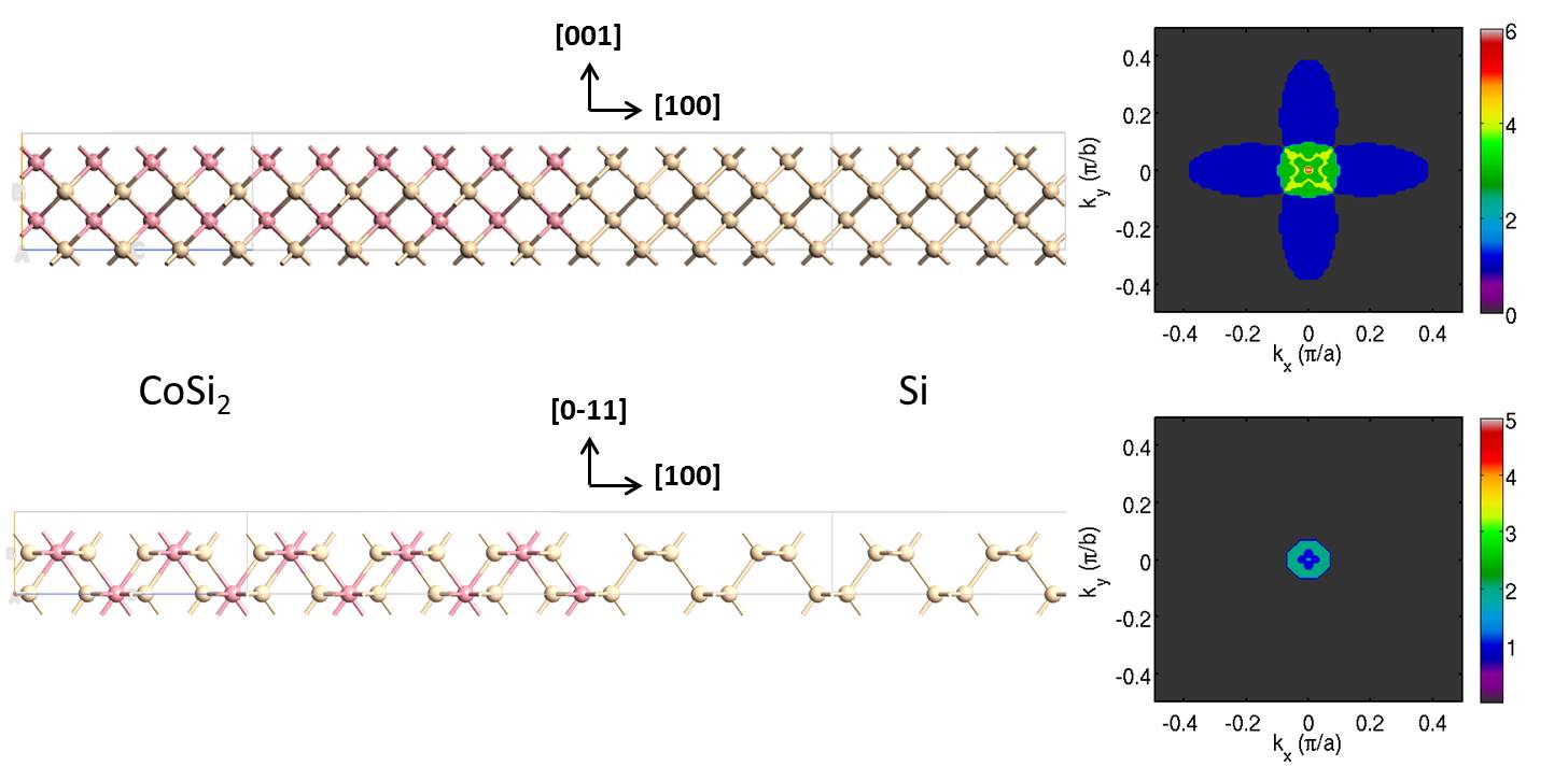
The assumptions made above ensure that a given transverse mode in Si (i.e. an allowed () value) conducts only if it is supplied by a conducting mode at the same transverse mode in CoSi2. These simplifying assumptions facilitate the study of electron transport across the CoSi2-Si interface in the limit of ballistic transmission while retaining an accurate representation of metal electronic structure. They also allow for a consistent calculation of the lower limits of specific contact resistivity, regardless of whether the metal is assumed to be ideal or not. Figure 2 shows the transmission spectra that arise as a result of such a coupling for the two interface orientations considered in this work.
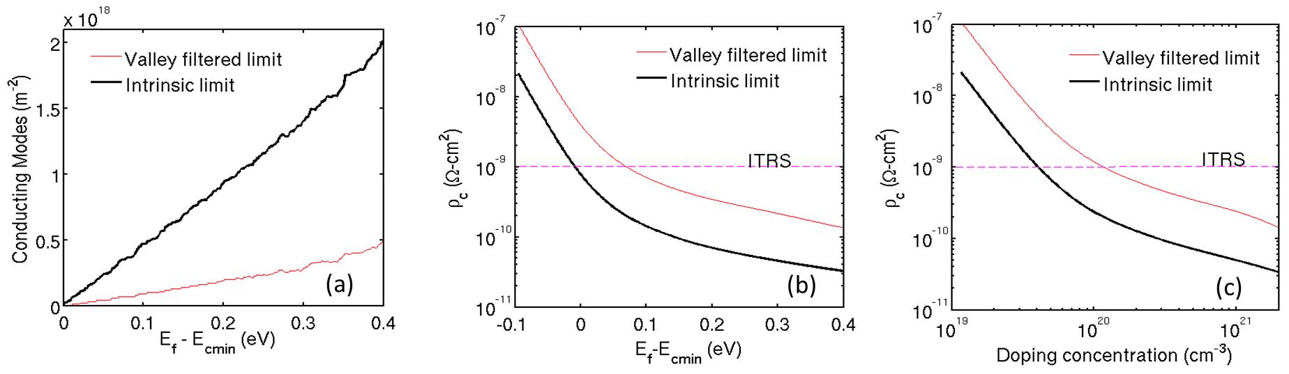
Once the transverse momentum-resolved transmission spectra for the coupled interface are computed under the assumptions outlined above, the number of available conducting modes per unit cross sectional area as a function of energy in Si, , is simply calculated as per the mode-counting formalism outlined in Maassen et al. Maassen et al. (2013).
| (1) |
From this information, the lower limit of single-contact resistivity com () of Si is computed in the Landauer formalism. Using the notation of Maassen et al.Maassen et al. (2013) this is given by
| (2) |
Here, is the Fermi-Dirac distribution function and is the fundamental quantum of conductance. In -Si, the occupancy of available conducting modes is modulated by donor doping (and temperature, assumed to be 300K throughout), which changes the Fermi level and consequently changes and . The precise dependence of the position of the Fermi level on doping concentration ( cm-3) is computed using the ATK package. The Si unit cell is populated by an additional negative charge corresponding to and compensated by a positive charge of the same amount to maintain neutrality. The Fermi Level is then computed by integrating the bulk band structure within the 1st BZ of the Si FCC unit cell using a uniform -grid of 203 points until the desired charge corresponding to is reached.
A very important consideration in interface transmission problems is that of momentum conservation. For interface transmission considered in this letter, where the boundary conditions transverse to the direction of transport are periodic, transverse momenta on either side of the interface are conserved. The allowed transverse momenta, however, are not the individual transverse momenta for the metal or semiconductor considered separately. Instead the allowed transverse momenta are determined by the non-primitive transverse interface unit cell vectorsBoykin and Klimeck (2005). Consequently, the allowed transverse momenta for the [100] oriented CoSi2-Si unit cells bound by the [010] and [001] directions in the TBZ are very different from those for the unit cell bound by [0-11] and [011] directions.
The importance of this feature for eventual interface electronic structure and transport cannot be overemphasized. Since the allowed momenta in the TBZ are strongly dependent on choice of unit cell vector, so is the transmission spectrum. This is very evident from Figure 1, where the constant energy ellipsoids in bulk Si close to the bottom of the conduction band get projected along different transverse directions. More importantly, this effect manifests as a significant change in the projection of the Fermi surface of CoSi2 on to the TBZ bound by the [010]/[001] and [0-11]/[011] orientations, respectively. The CoSi2 transmission spectrum in the [010]/[001] case (Figure 1(a)) overlaps with its corresponding Si transmission spectrum completely. In other words, the ’ideal metal’ assumption holds completely since every semiconducting mode is supplied by at least one mode from the metal. For the [0-11]/[011] case (Figure 1(b)), however, it is evident that the ’ideal metal’ assumption fails. The Si ellipses at the four corners of the TBZ find no supplying mode from the metal. The term ’valley filtering’ is therefore apt in this case and is a consequence of the metal being a non-ideal supplier of conducting modes into Si.
The effect of semiconducting valley-filtering on the transmission spectra of the coupled interfaces is shown in Figure 2. The only modes that conduct in the [0-11]/[011] bound coupled interface are the central modes that find supplying modes from the metal. In sharp contrast, the transmission spectrum of the [010]/[001] bound [100] coupled interface is identical to that in bulk Si. This effect is quantified in Figure 3. A significant reduction in the number of available modes for conduction is seen due to the valley filtering effect. From equation 2, it is evident that a reduction in the number of available modes adversely impacts contact resistivity, raising the minimum achievable contact resistivity in Si significantly. For instance, from Figure 3(c) it can be seen that at 71020cm-3, the minimum achievable in -Si increases a full order of magnitude from 610-11-cm2 to about 310-10-cm2 due to valley filtering in the [0-11]/[011] bound CoSi2-Si interface.
It must be reiterated that the calculated limits are reported assuming ballistic transmission across the interface. The presence of potential barriers of finite height and width, lattice imperfections and back-scattering at the interface due to effective mass mismatch between the metal and semiconductor will attenuate the transmission and consequently increase the contact resistivity considerably. Thus, while the ITRS requirement remains attainable at high doping concentrations, valley-filtering (if it does exist at a specific interface) in combination with the above limiting factors may prove to be a fundamental obstacle in improving contact resistivity.
It is important to recognize the limits of applicability of such an analysis. The electronic structure of metals changes considerably with confinement and strain Hegde et al. (2014a, b). This may affect valley filtering considerably. Also, the choice of simulation cell in this letter was guided by experiment. The simulation cells were chosen as the smallest lattice-matched unit cells obeying the 2D periodicity conditions indicated by the experiment. It is possible that other metal-semiconductor combinations have larger fundamental lattice-matched unit cells and different TBZ overlaps. For M-S combinations where experimental data is not available, the only alternative may be simulating interface formation through molecular dynamics (MD) simulations and then computing electronic transport on the resultant structures.
In conclusion, the lower limits of resistivity are computed in -Si for CoSi2-Si interface structures. It is shown that in some situations, the metal may behave ’non-ideally’ i.e. not supply conducting modes to the semiconductor equally throughout the TBZ. This effect is shown to be dependent on the specific interface chemistry simulated. The filtering of semiconducting valleys is shown to increase the minimum achievable contact resistivity in Si by an order of magnitude at high doping concentrations. While emphasizing the need to go beyond semi-classical and effective mass based electronic transport, the results highlight the need to revise the existing atomistic device simulation paradigm Fonseca et al. (2013), where metals are not explicitly included in the simulation. Including metals explicitly in atomistic DFT or TB simulations will ensure that effects such as valley filtering are incorporated into contact/device simulations.
From a technology perspective, these results indicate that in addition to metrics commonly understood to affect contact resistivity - SBH, barrier width, doping concentration, contact area - it is worth carefully considering if valley-filtering plays a role at the interface of a candidate metal-semiconductor interface.
The authors thank Jorge Kittl, Borna Obradovic, Ryan Hatcher and Mark Rodder for helpful discussions.
References
- itr (2011) “International technology roadmap for semiconductors - front end processes,” (2011).
- Yu (1970) A. Yu, “Electron tunneling and contact resistance of metal-silicon contact barriers,” Solid-State Electronics 13, 239–247 (1970).
- Griffiths (2013) D. J. Griffiths, Introduction to quantum mechanics: pearson new international edition (Pearson Education Limited, 2013).
- Maassen et al. (2013) J. Maassen, C. Jeong, A. Baraskar, M. Rodwell, and M. Lundstrom, “Full band calculations of the intrinsic lower limit of contact resistivity,” Applied Physics Letters 102, 111605–111605 (2013).
- Trumbore (1960) F. A. Trumbore, “Solid solubilities of impurity elements in germanium and silicon*,” Bell System Technical Journal 39, 205–233 (1960).
- Weber (2013) C. Weber, “The importance of metal transverse momentum for silicon contact resistivity,” Applied Physics Letters 103, 193505 (2013).
- Park et al. (2013) S.-H. Park, N. Kharche, D. Basu, Z. Jiang, S. Nayak, C. Weber, G. Hegde, K. Haume, T. Kubis, M. Povolotskyi, et al., “Scaling effect on specific contact resistivity in nano-scale metal-semiconductor contacts,” in Device Research Conference (DRC), 2013 71st Annual (IEEE, 2013) pp. 125–126.
- Gao and Guo (2012) Q. Gao and J. Guo, “Ab initio quantum transport simulation of silicide-silicon contacts,” Journal of Applied Physics 111, 014305 (2012).
- Tung, Schrey, and Yalisove (1989) R. Tung, F. Schrey, and S. Yalisove, “Homoepitaxial growth of cosi2 and nisi2 on (100) and (110) surfaces at room temperature,” Applied Physics Letters 55, 2005–2007 (1989).
- Boykin, Klimeck, and Oyafuso (2004) T. B. Boykin, G. Klimeck, and F. Oyafuso, “Valence band effective-mass expressions in the sp 3 d 5 s* empirical tight-binding model applied to a si and ge parametrization,” Physical Review B 69, 115201 (2004).
- Perdew, Burke, and Ernzerhof (1996) J. P. Perdew, K. Burke, and M. Ernzerhof, “Generalized gradient approximation made simple,” Physical review letters 77, 3865 (1996).
- atk (2014) “Atomistix toolkit version 13.8.0 quantumwise a/s quantumwise,” (2014).
- (13) “The itrs requirement for contact resistivity is for a single contact although contact resistivity measurements contain the effect of source and drain contact resistances,” .
- Boykin and Klimeck (2005) T. B. Boykin and G. Klimeck, “Practical application of zone-folding concepts in tight-binding calculations,” Physical Review B 71, 115215 (2005).
- Hegde et al. (2014a) G. Hegde, M. Povolotskyi, T. Kubis, J. Charles, and G. Klimeck, “An environment-dependent semi-empirical tight binding model suitable for electron transport in bulk metals, metal alloys, metallic interfaces, and metallic nanostructures. ii. application—effect of quantum confinement and homogeneous strain on cu conductance,” Journal of Applied Physics 115, 123704 (2014a).
- Hegde et al. (2014b) G. Hegde, M. Povolotskyi, T. Kubis, T. Boykin, and G. Klimeck, “An environment-dependent semi-empirical tight binding model suitable for electron transport in bulk metals, metal alloys, metallic interfaces, and metallic nanostructures. i. model and validation,” Journal of Applied Physics 115, 123703 (2014b).
- Fonseca et al. (2013) J. Fonseca, T. Kubis, M. Povolotskyi, B. Novakovic, A. Ajoy, G. Hegde, H. Ilatikhameneh, Z. Jiang, P. Sengupta, Y. Tan, et al., “Efficient and realistic device modeling from atomic detail to the nanoscale,” Journal of Computational Electronics 12, 592–600 (2013).
- Datta (1997) S. Datta, Electronic transport in mesoscopic systems (Cambridge university press, 1997).