Transport in two-dimensional disordered semimetals
Abstract
We theoretically study transport in two-dimensional semimetals. Typically, electron and hole puddles emerge in the transport layer of these systems due to smooth fluctuations in the potential. We calculate the electric response of the electron-hole liquid subject to zero and finite perpendicular magnetic fields using an effective medium approximation and a complimentary mapping on resistor networks. In the presence of smooth disorder and in the limit of weak electron-hole recombination rate, we find for small but finite overlap of the electron and hole bands an abrupt upturn in resistivity when lowering the temperature but no divergence at zero temperature. We discuss how this behavior is relevant for several experimental realizations and introduce a simple physical explanation for this effect.
pacs:
73.63.-b, 72.10.-d, 65.60.+a, 73.21.-bIn semimetals both electrons and holes contribute to transport. Typical examples are indirect bulk semiconductors with small band overlap. More recently also two-dimensional systems, including HgTe quantum wells close to the topological insulator to metal transition Kvon et al. (2008); Olshanetsky et al. (2009); Kvon et al. (2011); Olshanetsky et al. (2012, 2013), BiSe thin films Kastl et al. (2012), and bilayer graphene Feldman et al. (2009); McCann and Koshino (2013) have been identified to exhibit semimetallic properties. Electron and hole puddles typically emerge in the transport layer of these systems due to disorder that varies smoothly in space on a scale that is large compared to the mean free path of the charge carriers.

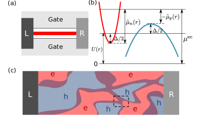
In this Letter, we introduce a two-fluid model to explore the effects of smooth disorder on the transport properties of two-dimensional electron-hole mixtures, Fig. 1. The model assumes that as a result of long-range correlated disorder, and a small intrinsic overlap between the electron and hole band, the sample at low temperatures can be divided into three types of regions: areas where only electron states or only hole states are occupied, and intermediate areas where both types of carriers are occupied, Fig. 1 (c). We assume that carriers are scattered easily within a band, due to phonons or residual impurities, but that recombination between electrons and holes is suppressed. Then, if neither the pure electron regions or pure hole regions percolate across the sample, charge transport at low temperatures may be effectively limited by the relatively narrow percolating portion where both electrons and holes are occupied and each carrier type has low density. As we shall see, this can lead to an anomalously high resistivity at low temperatures.
To make our picture quantitative, we introduce a model with smooth disorder, and obtain the local densities of electrons and holes using a Thomas-Fermi-like approximation. We assume that the electron and hole mobilities differ from each other, but are independent of the respective carrier densities. We solve the resulting inhomogeneous, two-component conductance problem using an effective medium approximation (EMA) Bruggeman (1935); Landauer (1952); Stroud (1975); Kirkpatrick (1973); Rossi et al. (2009); Tiwari and Stroud (2009). EMA has already been used successfully to characterize transport in GaAs quantum wells, where smooth disorder has been identified as the main mechanism for the transition from metallic to insulating behavior as a function of electron density Kravchenko et al. (1994); Meir (1999); Ilani et al. (2000); Meir (2000, 2001); Das Sarma et al. (2005); Tracy et al. (2009); Das Sarma et al. (2013). We investigate dependences of the transport on band-overlap, temperature, gate voltage, electron-hole recombination rate, and magnetic-field, using parameters we believe appropriate to the HgTe quantum wells in Ref. Olshanetsky et al. (2013). In the case of zero magnetic field, we checked the validity of EMA by introducing a model of resistors on a discrete lattice, which we solve numerically.
Quantum well at equilibrium.—We consider a two-dimensional electron and hole mixture with densities and , respectively. The characteristic correlation length scale of the disorder is set by the distance to charged impurities, which can typically be on the order of hundred nanometers. We expect this scale to be much larger than both the microscopic mean-free path of the charge carriers and the Coulomb screening length. Therefore, we will take a model in which we treat Coulomb interactions to be of the local form
| (1a) | ||||
| (1b) | ||||
where is the Coulomb kernel and is the effective Coulomb interaction parameter. The precise length scales of the screened Coulomb interaction and disorder potential do not enter into our analysis.
We define the energies in our description according to the level scheme illustrated in Fig. 1 (b):
| (2a) | ||||
| (2b) | ||||
where () is the electrochemical potential of the electrons (holes), [] is the electron [hole] chemical potential measured from the bottom of the conduction band [top of the valance band], and is the distance between the edges of the respective bands. Finite band overlap as indicated in Fig. 1 (b) corresponds to . The electrical potential is defined as , where describes the smooth spatial randomness of the potential on scale , which gives rise to the puddle formation, Fig. 1 (c).
At equilibrium the electrochemical potentials of the electrons and holes are identical, i.e., and determined by the gate voltage. Using Eqs. (1) and (2) we find
| (3a) | ||||
| (3b) | ||||
which have to be solved self-consistently in the presence of disorder as itself depends on the chemical potential .

Non-equilibrium treatment.—When a bias voltage is applied to the electrodes at the edges of the sample, the local potential changes in the entire sample thus causing a change of and . Out of equilibrium the bulk electron/hole electrochemical potentials therefore differ from each other
| (4a) | ||||
| (4b) | ||||
At the boundary the electrochemical potentials of both components are identical and fixed by the potential imprinted from leads .
The electron and hole currents are driven by the electrochemical potentials
| (5) |
where is the microscopic conductivity whose functional form we derive in the supplemental material from a Boltzmann transport formalism sup . In particular, we consider the linear current response of the two fluids to a small bias voltage. In that regime energy relaxation effects have not to be considered and thus we can assume that the system is locally at equilibrium. In our notation, and are vectors in the - plane, while are scalars, in the absence of an applied magnetic field.
The non-equilibrium dynamics of the electron-hole channels is decoupled, Eq. (5). However, recombination processes of rate dynamically couple the fluids, which can be taken into account by the continuity equation
| (6) |
Here, we used a two-component vector notation with the electron and hole component at the first and second entry, respectively. The steady state is obtained from the continuity equation by setting and boundary conditions that fix the electrochemical potential:
| (7) |
Solving (7) amounts to determining the conductance of a random medium. One approach is to discretize Eq. (7) and map it onto a resistor network, see supplemental material sup . Alternatively, one can exploit approximate features of such problems by a mean-field treatment, often referred to as EMA.
Cheianov, et al. Cheianov et al. (2007) have employed a resistor network model, similar in some respects to the one introduced here, to derive critical exponents and scaling behavior of graphene near its neutrality point. They use a percolation network analysis, which if applied to the present model, could be used to obtain the singular behavior in the limit where , , and tend to zero. In contrast, EMA predictions for the critical behavior would be qualitatively, but not quantitatively correct.
Effective medium approximation.—EMA considers inclusions, labeled with superscript , that are embedded in an effective medium, labeled with superscript . The embedding is determined self-consistently by requiring that the current in the effective medium is identical to the average current in the sample , for details see the supplemental material sup .
The resistivity can be evaluated from the total current response of the system. Considering that the electrochemical potential at the boundary is fixed (7), we define the total resistivity as with
| (8) |
where is the self-consistently determined conductivity matrix of the medium.
Resistivity of disordered HgTe quantum wells.—We now apply the method developed for a general disordered two-fluid model to HgTe quantum wells studied experimentally in Kvon et al. (2008); Olshanetsky et al. (2009); Kvon et al. (2011); Olshanetsky et al. (2012, 2013). In HgTe quantum wells a transition from a topological trivial insulator to a quantum spin Hall insulator can be driven by enhancing the thickness of the well Bernevig et al. (2006); König et al. (2007); Hart et al. (2014). When further increasing the width of the well the system undergoes another transition to a semimetallic phase in which both electron and hole carriers contribute to transport Kvon et al. (2008); Olshanetsky et al. (2009); Kvon et al. (2011); Olshanetsky et al. (2012, 2013). In the following, we consider 20nm HgTe quantum wells grown in the (100)-direction as studied in Ref. Olshanetsky et al. (2013). In that system, the effective electron and hole masses are very different Olshanetsky et al. (2012), a unit cell contains one electron and four hole pockets, and at atmospheric pressure the conduction and valance band overlap about meV to meV. In the experiment of Ref. Olshanetsky et al. (2013) hydrostatic pressure of kbar is applied to the sample which is expected to decrease the band overlap.
In accordance with these observations we choose the following parameters for our model: we set the Coulomb interaction parameter to , take into account the large difference in the effective electron and hole masses , and set . We sample the local potential from a uniform distribution of width , which we use as unit of energy. The disorder strength is renormalized by the effective screening parameter , where , yielding the effective disorder strength . Long-range disorder will influence the transport provided the band overlap . Based on these considerations, we choose two extreme limits for the band overlap and which should model zero and high pressure in experiment Olshanetsky et al. (2013). The studied HgTe quantum well has an indirect bandstructure in which the extrema of the conduction and valance bands are at different wave vectors, see Fig. 1 (b). The electron-hole recombination would therefore require phonon scattering which is suppressed at low temperatures. Thus we mostly consider zero carrier recombination rate .

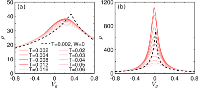
In Fig. 2 we show the resistivity obtained from EMA as a function of the gate voltage which directly modifies the electrochemical potential in Eq. (3). In accordance with the experiment Olshanetsky et al. (2013) we observe metallic behavior for , with a weak dependence on temperature only (a). The asymmetry in the curves with respect to arises due to the large difference in electron and hole masses. For comparison we show the pure case , dashed lines. For reduced band overlap and at , the resistivity increases strongly at low temperatures while at high temperatures the system remains conducting (b). Further the maximum in the resistivity is shifted toward lower gate voltage. These results qualitatively explain several features of the HgTe quantum well experiments of Ref. Olshanetsky et al. (2013).
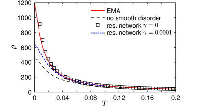
The enhancement of the resistivity at low temperatures and the flattening out at high temperatures is demonstrated in Fig. 3 for a fixed gate voltage . In this plot we compare the results obtained within EMA to the solution of a resistor network sup of size for vanishing electron-hole recombination rate and find good agreement. Finite decreases the sharp low-temperature feature. We also compare the resistivity of the disordered systems to the resistivity of the clean system and find an enhancement at low temperatures, which is one of the main observations of our work.
A percolation picture provides further insights. When the recombination rate is very small, we must compute separately the conserved currents of electrons and holes, and add the results in the end. Let us consider the electron conductance as an example. If the band overlap is small, and the system is electrically neutral, then the regions where only electrons exist at will not percolate across the sample. In order to get from one of these regions to another, an electron has to cross the intermediate region, where electrons and holes coexist, which will generally occur at isolated junctions, where the two electron puddles come close together, see e.g. dashed rectangle in Fig. 1 (c). The conductance of these junctions will be small, since they occur at places where the electron and hole densities are both nearly vanishing. The resistance of the electron network will be dominated by these junctions, and in fact it will diverge in the limit where the overlap goes to zero and there are equal numbers of electrons and holes. By contrast, at high temperatures, there will be a large number of thermally excited electrons and holes even in the regions separating the electron and hole dominated areas, so carriers can get across the sample without crossing a region of low conductivity. This physics is correctly captured by EMA.
Resistivity in the presence of magnetic field.—To understand the relative electron and hole dominance we study the magnetotransport for fields applied perpendicular to the transport layer. The model we derived for a setting with zero magnetic field is readily generalized to finite magnetic fields, see supplemental material sup with the key difference that the resistivity has a tensorial structure consisting of a longitudinal and a transverse contribution Abrikosov (1972); Bergman and Strelniker (1999).

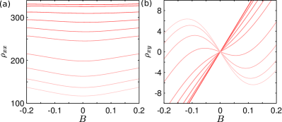
In Fig. 4 we show the (a) longitudinal and the (b) transverse resistivity as a function of magnetic field for fixed gate voltage . We find that the longitudinal resistivity increases with magnetic field and decreases with temperature . For the chosen gate voltage the sign of the Hall charge (i.e., the slope of at ) changes with temperature. The gate voltage is adjusted such that at low temperatures holes are the dominating charge carriers. With increasing temperature percolating paths open up faster for the light electrons as compared to the heavy holes. Thus the electrons dominate transport at high temperatures leading to the change of the Hall charge.
Conclusions and outlook.—We developed a theory for transport in long-range disordered two-fluid systems as realized for instance in semimetallic quantum wells, thin films, and bilayer graphene.
We applied the developed technique to study transport in HgTe quantum wells and found that it captures several characteristic features observed in experiment Olshanetsky et al. (2013) including the strong enhancement of the resistivity at low temperatures near charge neutrality. In Ref. Olshanetsky et al. (2013) the authors proposed an alternative explanation of this effect based on the phase transition to an excitonic insulator at low temperatures which does not consider long-range disorder but rather requires strong interactions. In contrast, in our theory which identifies long-range disorder as a crucial mechanism, the sharp enhancement of the resistivity is not indicative of a true phase transition. At low temperatures the resistivity will rather saturate, albeit at a very large value. This feature is generic for semimetals with small band overlap and results from (i) the relatively small percolating portion of coexisting electron and hole states and (ii) the vanishing electron-hole recombination rate relevant to the indirect bandstructures, such as the one of the considered HgTe quantum well.
This leads us to the conclusion that large length-scale disorder is a central mechanism in these experiments. Of course a complex interplay between long-range disorder and interactions is conceivable as well. Further experimental studies are therefore needed to fully confirm the picture. In particular, it would be interesting to explore the resistivity as a function of the applied pressure, which should tune the band overlap continuously, and thus allow to study the emergence of the strong enhancement of the resistivity at low temperatures.
Acknowledgements.—We thank D. Kvon for introducing us to this problem and for sharing experimental results prior to publication. The authors acknowledge support from Harvard-MIT CUA, ARO-MURI Quism program, ARO-MURI on Atomtronics, STC Center for Integrated Quantum Materials, NSF grant DMR-1231319, as well as the Austrian Science Fund (FWF) Project No. J 3361-N20.
References
- Kvon et al. (2008) Z. D. Kvon, E. B. Olshanetsky, D. A. Kozlov, N. N. Mikhailov, and S. A. Dvoretskii, JETP Lett. 87, 502 (2008).
- Olshanetsky et al. (2009) E. B. Olshanetsky, Z. D. Kvon, M. V. Entin, L. I. Magarill, N. N. Mikhailov, I. O. Parm, and S. A. Dvoretsky, JETP Lett. 89, 290 (2009).
- Kvon et al. (2011) Z. D. Kvon, E. B. Olshanetsky, E. G. Novik, D. A. Kozlov, N. N. Mikhailov, I. O. Parm, and S. A. Dvoretsky, Phys. Rev. B 83, 193304 (2011).
- Olshanetsky et al. (2012) E. B. Olshanetsky, Z. D. Kvon, N. N. Mikhailov, E. G. Novik, I. O. Parm, and S. A. Dvoretsky, Solid State Commun. 152, 265 (2012).
- Olshanetsky et al. (2013) E. B. Olshanetsky, Z. D. Kvon, Y. A. Gerasimenko, V. Prudkoglyad, V. Pudalov, N. N. Mikhailov, and S. A. Dvoretsky, Pis’ma v ZhETF 98, 947 (2013).
- Kastl et al. (2012) C. Kastl, T. Guan, X. Y. He, K. H. Wu, Y. Q. Li, and A. W. Holleitner, Appl. Phys. Lett. 101, 251110 (2012).
- Feldman et al. (2009) B. E. Feldman, J. Martin, and A. Yacoby, Nat. Phys. 5, 889 (2009).
- McCann and Koshino (2013) E. McCann and M. Koshino, Rep. Prog. Phys. 76, 056503 (2013).
- Bruggeman (1935) D. A. G. Bruggeman, Ann. Phys. (Leipz.) 416, 636–664 (1935).
- Landauer (1952) R. Landauer, J. Appl. Phys. 23, 779 (1952).
- Stroud (1975) D. Stroud, Phys. Rev. B 12, 3368 (1975).
- Kirkpatrick (1973) S. Kirkpatrick, Rev. Mod. Phys. 45, 574 (1973).
- Rossi et al. (2009) E. Rossi, S. Adam, and S. Das Sarma, Phys. Rev. B 79, 245423 (2009).
- Tiwari and Stroud (2009) R. P. Tiwari and D. Stroud, Phys. Rev. B 79, 165408 (2009).
- Kravchenko et al. (1994) S. V. Kravchenko, G. V. Kravchenko, J. E. Furneaux, V. M. Pudalov, and M. D’Iorio, Phys. Rev. B 50, 8039 (1994).
- Meir (1999) Y. Meir, Phys. Rev. Lett. 83, 3506 (1999).
- Ilani et al. (2000) S. Ilani, A. Yacoby, D. Mahalu, and H. Shtrikman, Phys. Rev. Lett. 84, 3133 (2000).
- Meir (2000) Y. Meir, Phys. Rev. B 61, 16470 (2000).
- Meir (2001) Y. Meir, Phys. Rev. B 63, 073108 (2001).
- Das Sarma et al. (2005) S. Das Sarma, M. P. Lilly, E. H. Hwang, L. N. Pfeiffer, K. W. West, and J. L. Reno, Phys. Rev. Lett. 94, 136401 (2005).
- Tracy et al. (2009) L. A. Tracy, E. H. Hwang, K. Eng, G. A. Ten Eyck, E. P. Nordberg, K. Childs, M. S. Carroll, M. P. Lilly, and S. Das Sarma, Phys. Rev. B 79, 235307 (2009).
- Das Sarma et al. (2013) S. Das Sarma, E. H. Hwang, and Q. Li, Phys. Rev. B 88, 155310 (2013).
- (23) See supplementary online material.
- Cheianov et al. (2007) V. V. Cheianov, V. I. Fal’ko, B. L. Altshuler, and I. L. Aleiner, Phys. Rev. Lett. 99, 176801 (2007).
- Bernevig et al. (2006) B. A. Bernevig, T. L. Hughes, and S.-C. Zhang, Science 314, 1757 (2006).
- König et al. (2007) M. König, S. Wiedmann, C. Brüne, A. Roth, H. Buhmann, L. W. Molenkamp, X.-L. Qi, and S.-C. Zhang, Science 318, 766 (2007).
- Hart et al. (2014) S. Hart, H. Ren, T. Wagner, P. Leubner, M. Mühlbauer, C. Brüne, H. Buhmann, L. W. Molenkamp, and A. Yacoby, Nat. Phys. 10, 638 (2014).
- Abrikosov (1972) A. A. Abrikosov, Introduction to the Theory of Normal Metals (Academic Press, New York, USA, 1972).
- Bergman and Strelniker (1999) D. J. Bergman and Y. M. Strelniker, Phys. Rev. B 60, 13016 (1999).