∎
CNRS, Institut N éel, Grenoble, France
77email: herve.courtois@neel.cnrs.fr, 44institutetext: H. Q. Nguyen 55institutetext: Université Grenoble Alpes, Institut N éel, Grenoble, France
CNRS, Institut N éel, Grenoble, France
O.V. Lounasmaa Laboratory, Aalto University, Helsinki, Finland 66institutetext: F. W. J. Hekking 77institutetext: Université Grenoble Alpes, LPMMC, Grenoble, France
CNRS, Institut N éel, Grenoble, France
Electronic coolers based on superconducting tunnel junctions: fundamentals and applications
Abstract
Thermo-electric transport at the nano-scale is a rapidly developing topic, in particular in superconductor-based hybrid devices. In this review paper, we first discuss the fundamental principles of electronic cooling in mesoscopic superconducting hybrid structures, the related limitations and applications. We review recent work performed in Grenoble on the effects of Andreev reflection, photonic heat transport, phonon cooling, as well as on an innovative fabrication technique for powerful coolers.
pacs:
74.78.Na 74.45.+c1 Introduction
Let us consider a NIS tunnel junction made of a Normal metal and a Superconductor, in contact through an Insulator barrier. The superconductor’s electronic density of states features an energy gap of width . Tunneling through the junction is possible for electrons with an energy (compared to the Fermi level ) such that . Only elastic processes are considered here. The charge current through such a junction biased at a voltage is TinkhamBook :
| (1) | |||
| (2) |
where is the normal state resistance, the electron energy distribution in the normal metal and the normalized BCS density of states in the superconductor. No Dynes parameter smearing the superconductor’s density of states is taken into account. Expression (1) above is the usual one, while expression (2) can be obtained by a symmetry argument. The latter shows that the current does not depend on the superconductor temperature, only on the value of the gap.
When using it as a thermometer NahumAPL93 , a NIS junction is biased at a small and constant current . The current can be adjusted so that the related heat flow (see below) can be safely neglected. The voltage drop in the thermometer junction pair is then measured and compared to its value calibrated against the bath temperature . This provides a measure of the electronic temperature with a sub-mK resolution. Let us note that the calibration is realized at equilibrium, with the superconductor and the normal metal being at the bath temperature. In contrast, practical experiments are usually conducted in quasi-equilibrium conditions where, to a first approximation, only the normal metal temperature changes. If one considers temperatures above about half the superconductor critical temperature , the related decrease of the superconductor gap has to be taken into account. The calibration then requires the full calculation of the voltage using Eq. (2).
The same tunnel current can cool down or heat up the normal metal electron population NahumAPL94 ; LeivoAPL96 . The heat current through a NIS junction reads:
| (3) |
where is the energy distribution function in the superconductor. Equation 3 differs from Eq. 1 by an additional energy term in the integral, which also changes the symmetry compared to the charge current case: while . Equation 3 describes both the cooling and heating regimes. With a voltage bias smaller than the gap , the tunnel current is selectively made out of high-energy electrons (or holes) from the tails of the distribution function. This cools the electronic population of the normal metal, which means that is positive. Every tunnel event extracts a heat of about while a heat is dissipated in the system, so that the cooling efficiency is about . Above the gap (), the heat flow becomes negative (the metal is heated). At large bias , the usual Joule heating regime is reached, is equal to . In every case, the full Joule power is deposited in the device, so that a power is transferred to the superconductor.
In the cases studied here, we assume a quasi-equilibrium situation: the normal metal electrons and phonons follow thermal energy distribution functions at respective temperatures and . For electrons, this is justified because the inelastic scattering time (of the order of the phase-coherence time) is much shorter than the mean residence time estimated to about 100 ns for an island of typical dimension 50 nm 1 m2 JLTP-Rajauria . The thermalization of an isolated normal metal electron population to the thermal bath occurs through electron-phonon coupling. We will make use of the standard expression:
| (4) |
of the electron-phonon coupling power, where is a material-dependent constant and is the metal volume. Several experiments have demonstrated the validity of this expression in mesoscopic (micron-sized) devices PRB-Urbina ; JLTP-Godfrin , although it is derived for a bulk material. In what follows, we take for Cu the established value = 2 nW.m-3.K-5.
Although electronic cooling can be obtained in a single NIS junction where the normal metal is isolated from its electrical contact pad by the way of a thermally-insulating NS contact NahumAPL94 , the symmetric SINIS configuration with two NIS junctions acting as coolers brings the advantage of simplicity and a doubled cooling power LeivoAPL96 . Thanks to the current singularity at the gap edge, the SINIS geometry is rather immune to a small junctions’ resistance asymmetry PhysicaPekola .
The above considerations form the basis for electronic cooling. This topic has been discussed in recent reviews GiazottoRMP06 ; MuhonenRPP12 . Starting from a bath temperature of about 300 mK, an electronic temperature reduction by a factor of about 3 is routinely achieved in aluminum-copper hybrid devices that are biased at a voltage just below the gap of superconducting Al. The cooling power is in the 10 pW range for a tunnel junction area of about a square micron. Micro-coolers based on large lithographic junctions patterned on a membrane have demonstrated the cooling a bulk material ClarkAPL04 or a detector MillerAPL08 . Exciting new developments towards larger cooling powers NguyenNJP13 and cooling of macroscopic objects LowellAPL13 are emblematic of the present activity in the field.
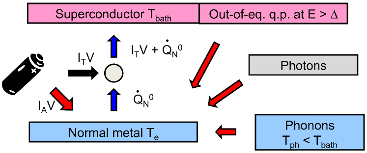
In practice, electronic cooling in a normal metal is limited by several mechanisms of fundamental interest, see Fig. 1. Electron-phonon scattering provides the main channel for thermalization of the electronic bath with respect to the substrate considered to be a thermal bath. The question of phonon cooling is therefore of primary importance. In recent years, we have also studied how other channels of thermalization contribute. In the following, we will discuss how Andreev current or photonic heat channel alter the electronic cooling in a SINIS device. We will not discuss quasi-particle relaxation in the superconducting electrodes, although it is a major and long-standing issue PekolaAPL00 ; RajauriaPRB09 ; PRB12-Rajauria .
2 Methods
We study SINIS samples based on a normal metal island symmetrically coupled to two superconducting leads through tunnel barriers, see Fig. 2a. In general, they are prepared by electronic beam lithography on a resist bilayer, followed by two-angle evaporation in a high vacuum chamber CourtoisPRB95 . We focus on aluminium as a superconductor because of its unique high-quality oxide. As a thin film, its critical temperature is about 1.3 K. The normal metal is usually copper, with a diffusion constant of about 100 . The total normal-state resistance is in the range 2-3 k for a tunnel junction area of about 1 . In addition to the two cooling junctions, one can add superconducting tunnel probes in order to probe the normal metal electronic temperature. In one case, we have built two such complete devices one on top of the other, in order to study the phonon bath behavior.
Low temperature measurements were performed in a 3He cryostat or a dilution cryostat. Filtering was provided by -filters at room temperature and lossy micro-coaxial lines thermalized at the cold plate. Four-wire d.c. transport measurements were performed using home-made electronics combining independent current bias sources, one of them providing the voltage reference, the other being floating. The differential conductance is obtained by numerical differentiation. We have taken special care to determine most accurately the sub-gap conductance of our current-biased samples down to a level of about of the normal state conductance. Plots are usually a combination of multiple curves covering different measurement ranges, extending over several decades of current values. Semi-log plots are useful to provide a good understanding of the charge and heat transport. In such a plot, the sub-gap differential conductance of a NIS junction at constant temperature follows a linear behavior with the voltage drop. This comes from the fact that the Fermi distribution function of the energy can be approximated to a decaying exponential at energies well above or below the Fermi level.
In order to understand some of the experimental observations, we have investigated theoretically various aspects of heat and charge transport in NIS tunnel junctions. Since the devices measured experimentally are in the diffusive limit, the appropriate theoretical framework to describe thermo-electric transport is based on quasi-classical Keldysh-Usadel equations Larkin86 ; Belzig99 . Specifically, using this formalism, we have calculated the two-particle current due to Andreev reflection VasenkoPRB10 . This is relevant for the experiments discussed in Section 3 below. We also considered the effect of inelastic relaxation in the superconductor lead VasenkoJLTP . In the absence of strong relaxation, both the electric current and the cooling power at low voltages are suppressed. We could attribute this suppression to the effect of back-tunneling of non-equilibrium quasiparticles from the superconductor into the normal metal, a topic relevant for the experiments described in Section 5 below.
3 Heating induced by the Andreev current
Operation and limitations of NIS electronic coolers in the low-temperature regime () have been questioned in the past PRL-Pekola . A residual smearing of the superconductor density of states has been proposed as the origin of the inferior performance with respect to theoretical expectations.
At low energy , charge transfer at a NIS interface occurs through Andreev reflection Andreev ; SaintJames . In the normal metal, an electron (a hole) impinging on the superconducting interface is reflected as a hole (an electron), enabling the transfer of a Cooper pair into (out of) the superconductor. For a NIS tunnel junction of intermediate or low transparency, the Andreev reflection probability is predicted to be vanishingly small. Taking into account the quasi-particles confinement in the vicinity of the interface, this is no longer true. This confinement can be induced by disorder or the presence of a second barrier in the normal metal. A single quasiparticle then experiences several collisions with the interface PRL-VanWees ; PRL-Hekking so that the actual Andreev reflection transmission coefficient corresponds to the coherent addition of many individual transmission probabilities. Therefore, the Andreev sub-gap current can significantly exceed the ballistic case prediction PRL-Kastalsky .
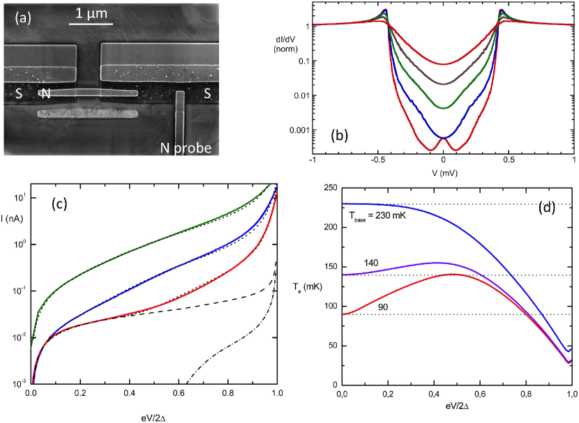
Fig. 2b displays on a logarithmic scale the differential conductance of a SINIS device for a series of cryostat temperatures RajauriaPRL08 . We observe in the high temperature ( 200 mK) data an upward curvature which constitutes a clear signature of electronic cooling. In the low temperature regime ( 200 mK), clearly a different characteristic is obtained with a differential conductance peak at zero bias. The zero-bias differential conductance increases while the temperature is lowered below about 200 mK. We ascribe the low bias differential conductance peak to an Andreev current, i.e. a double particle tunnel current created by Andreev reflections at the NIS junctions.
In order to calculate the Andreev current, we take into account the finite gap and the disorder both in the normal metal and in the superconductor. We consider the 1D regime where the coherence length of an Andreev pair in the normal metal Superlattices-Courtois is much larger than the junction dimension. Usadel equations formalism can also be used and provide the same result VasenkoPRB10 . In the probe junction, the electronic temperature can be considered as constant and very close to the cryostat temperature. In this case, the isothermal calculation fits nicely the experiment (not shown). In the cooler junction, the non-linear behavior in a semi-log scale (Fig. 2c) shows that electronic cooling (and heating) has to be taken into account.
The work performed by the current source feeding the circuit with a (Andreev) current generates a Joule heating that is deposited in the normal metal. The full heat balance equation for the normal metal electrons can then be written as:
| (5) |
Here the factor 2 accounts for the presence of two tunnel junctions. In the low-temperature limit considered here, the normal metal phonons can be considered as thermalized at the bath temperature: . With this complete heat balance equation taken into account, we calculate the current-voltage characteristic at every cryostat temperature. The agreement is very good at every temperature, see Fig. 2c, and covers 4 orders of magnitude for the current. At temperatures above about 300 mK, phonon cooling introduces significant corrections, see below.
The numerical solution of the heat balance equations also provides the electron temperature at every bias. Fig. 2d shows the calculated dependence of the normal metal central island electron temperature with the voltage across the cooler. At very low temperature, the electron temperature first increases with the bias due to Andreev current heating, before decreasing due to the single quasi-particle tunnel current-based cooling effect. Although the Andreev current is a small effect in a such junction if one considers the charge current, this is no longer true if one considers the heat current. Compared to a Joule power , the Andreev current contributes fully to heating while the tunnel current cools with a moderate efficiency of about 5 at a 100 mK electron temperature.
4 Photonic heat channel
In metallic systems, heat conduction can be achieved by electrons, phonons and also photons. The photonic channel Schmidt04 was recently revealed experimentally Nature-Meschke ; PRL-Timofeev-1 at very low temperature in devices including superconducting transmission lines. With a good matching between the source and the drain, the thermal conductance of a superconducting transmission line is equal to the thermal conductance quantum Pendry83 : . The photonic channel for heat transfer can in principle couple metallic systems that are galvanically isolated, e.g. through a capacitor, or weakly coupled, e.g. through a tunnel junction. This effect can be beneficial in some cases, but also detrimental when one wants to maintain two electronic populations at different quasi-equilibrium temperatures. This is precisely the case encountered in electronic coolers.
We have investigated theoretically the photonic heat transfer through a general reactive impedance, i.e. a linear coupling circuit that contains a capacitor, an inductance, a resonant circuit or a transmission line PascalPRB11 . Only the case of a capacitor will be discussed here, but the same approach can be used in all cases. We follow a simple circuit approach Beenakker03 , valid at low temperatures when the relevant photons have wavelengths larger than the size of the typical circuit element. The metallic parts can then be treated as lumped elements characterized by an electrical impedance.
Let us consider a circuit of two pure resistors 1 and 2 of resistance coupled capacitively through an impedance , see Fig. 3b inset. With a small temperature difference and using the dimensionless frequency
| (6) |
the exchanged power and the thermal conductance are given by:
| (7) |
taking into account the frequency-dependent photon transmission coefficient:
| (8) |
The cross-over frequency is determined by the parameter
| (9) |
it separates a low-frequency regime where the capacitor is opaque and from a high-frequency regime where the capacitor is transparent and .
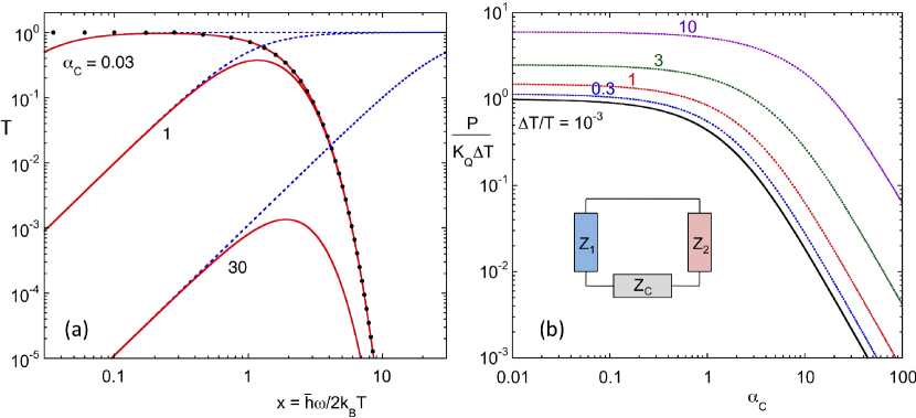
Fig. 3a displays the photon transmission coefficient . The limit means that the capacitance is large, i.e. it has a negligible impedance over most of the thermal spectrum. The transparency is then equal to unity and one recovers . In the limit , the photonic signal is strongly suppressed by the RC filter composed of the series capacitance and the receiver resistance, leading to .
The total photonic power, integrated over the full frequency range, is shown in Fig. 3b as a function of the parameter . We compare both linear and non-linear response, changing the values of the relative temperature difference . The total power is maximal for small ; it decays as when is large. A cross-over between the linear regime and the non-linear regime occurs at . When the temperature difference is large, the photonic thermal conductance is larger than its quantum because of the broader frequency range of the emitted photons. Nevertheless, the thermal conductance remain of the order of , i.e. 1 pW/K at 1 K, and thus little contributes in usual situations.
5 Phonon cooling
As mentioned above, the electron-phonon coupling provides the main channel for coupling of the cooled electron population to the thermal bath of the cryostat. The question arises of the actual temperature of the phonon bath in the normal metal. At a temperature , phonons have a thermal wavelength of the order of , where is the material-dependent sound velocity. This dominant wavelength amounts to about 200 nm in Cu at 1 K, which is the order of magnitude of an usual device dimensions. It is thus generally assumed that phonons in a mesoscopic quantum device are strongly mixed with the substrate phonons and are thus thermalized at the bath temperature GiazottoRMP06 .
Nevertheless, phonon cooling is at the heart of the possibility of cooling a bulk detector ClarkAPL05 or a quantum device VercruyssenAPL11 supported on a membrane cooled by superconducting tunnel junctions. The same situation also holds for suspended metallic beams KoppinenPRL09 ; MuhonenAPL09 . Recently, measurements of the electron-phonon coupling strength in a thin metallic film at T 0.1-0.3 K demonstrated that it is nearly completely substrate-insensitive UnderwoodPRL11 . This supports the idea of an independent phonon population in the metallic thin film. While this phonon bath could exhibit specific properties due to its reduced dimensionality QuPRB05 ; HekkingPRB08 , only small deviations from bulk material properties were observed in suspended devices KarvonenPRL07 .
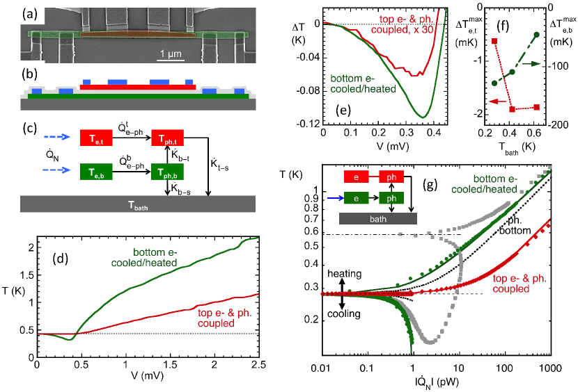
We have devised a dual-level sample with two independent but stacked SINIS devices including electron thermometers, see Fig. 4a. The experiment PascalPRB13 consists in current-biasing one of the two level’s cooler junction pair while monitoring simultaneously the related voltage drop as well as the two levels’ electronic temperatures and , where ”b” stand for bottom and ”t” for top. As no power is directly injected in the unbiased electronic bath, its temperature is equal to the included metal’s phonon temperature. For voltages below applied to the bottom level, we observe the expected electronic cooling, see Fig. 4d. At voltages above , we observe a hot-electron regime: the temperature increases and goes well above the bath temperature of 432 mK.
Remarkably, when the bottom level electronic temperature decreases, the top electronic temperature also diminishes with a variation reaching a maximum of - 2.0 mK, see Fig. 4e. As the operation of the electronic cooler is dissipative as a whole, i.e. heat is dissipated in the chip, this observation cannot be related to an improper thermalization of the chip or of electrical leads. The observed cooling of the top level therefore demonstrates phonon cooling in the normal conductors of the experiment.
The cooling/heating power was calculated by using Eq. 3, the measured electronic temperature, and a value 214 . As a fraction of the hot quasi-particles injected in the superconductor tunnels back in the normal metal, we have described this as a correction to the power proportional to UllomPhysica00 : the net power then writes . The fit parameter value = 0.087 is comparable to what appears in the literature UllomPhysica00 . The electronic temperature as a function of the net power absolute value then follows a single curve when one goes through the maximum cooling point, see Fig. 4g.
We consider a thermal model, see Fig. 4c, assuming two distinct phonon populations at quasi-equilibrium at temperatures and in the bottom and top metallic islands respectively. We assume that two neighbouring phonon populations (here x and y) are coupled through a Kapitza heat flow of the form
| (10) |
GiazottoRMP06 , where holds for the contact area between the two considered populations and is an interface materials-dependent parameter. We have chosen to take a common value for the substrate-bottom and bottom-top Kapitza parameters. The fit-derived value = 45 pW.m-2.K-4 compares well to values from the literature for a Cu-Si interface SwartzRMP89 . As for the top-substrate coupling, considering the contact area to be the area of the tunnel junctions connected to the island, one obtains a Kapitza coefficient of 920 pW.m-2.K-4, which is much larger than anticipated. Thus the heat transfer occurs presumably also along the continuous Si layer separating the two levels, which explains the relatively modest amplitude of the observed phonon cooling.
From the thermal balance relations, one can calculate the phonon temperature variation in the cooled or heated metal, see dotted lines in Fig. 4g. The phonon population temperature decoupling is significant in the temperature range 0.3 - 1 K, consistently with previous estimates RajauriaPRL07 . At lower temperature, the electron-phonon bottle-neck makes the phonon temperature tend to the bath temperature. At a bath temperature below 100 mK, phonon cooling becomes negligable.
Our experimental study thus demonstrates the existence of an independent phonon bath in a quantum device. The thermal couplings are well described with the usual laws for electron-phonon coupling and Kapitza resistances. This new understanding has significant outcomes in the analysis of quantum nano-electronic devices thermal behavior.
6 Towards large electronic cooling power
Optimizing a SINIS device for electron cooling can be achieved by increasing the heat current and/or isolating better the cooled electron bath. As the heat current is proportional to the tunnel barriers’ conductance, reducing the barriers’ thickness is the first option. Nevertheless, this can lead to the appearance of two-particle Andreev reflection processes at low energy, which deposit heat in the normal metal RajauriaPRL08 . The obvious alternative is to increase the junction area at a fixed transparency ONeilPRB12 . We present a method to fabricate large area SINIS devices of high quality and with a suspended normal metal NguyenAPL12 . The method is based on a pre-deposited multilayer of metals, which can be prepared at the highest quality. The upper normal part is suspended in the first lithography, which keeps it isolated from the substrate. The second lithography defines the junction area with any geometry of interest.
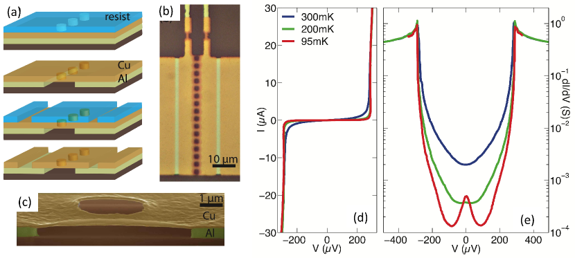
The fabrication starts with depositing a Al/AlOx/Cu multilayer on an oxidized silicon substrate. A first deep ultra-violet lithography is used to define the overall device geometry. The central part is a series of adjacent holes of diameter 2 m and with a side-to-side separation of 2 m, see Fig. 5b. The copper layer is etched away over the open areas using either Ion Beam Etching (IBE) or wet etching. The aluminum is then etched through the same resist mask, using a weak base. The etching time is controlled as to completely remove aluminum from the circular region within a horizontal distance of about 2 m starting from the hole side. The line of adjacent holes visible in Fig. 5b therefore creates a continuous gap in the Al film, bridged only by a stripe of freely hanging Cu. The area of the NIS junctions is defined by a second lithography. Through the open areas, trenches are etched into the copper layer only, using one of the two methods cited above. These trenches allow to isolate a copper island, which forms the central normal metal part of the SINIS device.
Fig. 5d,e shows the current-voltage characteristic and the numerically-derived differential conductance of a typical sample at various cryostat temperatures. We have measured the electronic temperature as a function of the cooler voltage bias by using the two attached smaller junctions, see Fig. 5b, as an electron thermometer. At a bath temperature of 300 mK and at the optimum bias point, the measured electronic temperature reaches a minimum of 240 mK.
Removing the contact between the substrate and the cooled metal by suspending the latter is quite promising for electronic refrigeration applications as it can significantly improve cooling of electrons and phonons. Our approach also has the advantage that as fabrication starts with preparing the multilayer, the wafer can be baked in ultra-high vacuum environment, which is an essential ingredient for obtaining pinhole-free large-area NIS junctions. This process has recently been improved by including a quasi-particle drain in good contact with the superconducting electrodes. A nanoWatt cooling power NguyenNJP13 as well as a base temperature down to 30 mK have been demonstrated NguyenUnpublished . This high performance can be understood only by assuming some phonon cooling in the suspended metal.
7 Conclusion
As a summary, we have reviewed a series of experimental studies combined with theoretical analyses of different phenomena at work in SINIS electronic coolers. Andreev current heating, coupling to phonons, phonon cooling, photonic coupling are all important limiting factors and either can dominate, depending on the practical case. The field is in constant progress, for example with the demonstration of improved performance NguyenNJP13 and suitability for the cooling of macroscopic objects LowellAPL13 .
Acknowledgements.
This work was funded by the EU FRP7 low temperature infrastructure MICROKELVIN and by Institut universitaire de France. Samples were fabricated at Nanofab platform - CNRS. This work has been led in collaboration with S. Rajauria, L. M. A. Pascal, A. Fay, B. Pannetier, A. Vasenko, T. Crozes and T. Fournier. We acknowledge fruitful discussions along the years with J. P. Pekola, F. Giazotto and M. Meschke.References
- (1) M. Tinkham, Introduction to Superconductivity, Mc-Graw Hill (1996).
- (2) M. Nahum and J. Martinis, Appl. Phys. Lett. 63, 3075 (1993).
- (3) M. Nahum, T. M. Eiles, and J. M. Martinis, Appl. Phys. Lett. 65, 3123 (1994).
- (4) M. M. Leivo, J. P. Pekola, and D. V. Averin, Appl. Phys. Lett. 68, 1996 (1996).
- (5) H. Courtois, S. Rajauria, P. Gandit, F. W. J. Hekking and B. Pannetier, J. of Low Temp. Phys. 153, 325 (2008).
- (6) F. C. Wellstood, C. Urbina, and J. Clarke, Phys. Rev. B 49, 5942 (1994).
- (7) M. Meschke, J. P. Pekola, F. Gay, R. E. Rapp, H. Godfrin, J. of Low Temp. Phys. 134, 1119 (2004) and references therein.
- (8) J. P. Pekola, A. J. Manninen, M. M. Leivo, K. Arutyunov, J. K. Suoknuuti, T. I. Suppula, and B. Collaudin, Physica B 280, 485 (2000).
- (9) F. Giazotto, T. T. Heikkilä, A. Luukanen, A. M. Savin and J. P. Pekola, Rev. Mod. Phys. 78, 217 (2006).
- (10) J. T. Muhonen, M. Meschke, and J. P. Pekola, Rep. Prog. Phys. 75, 046501 (2012).
- (11) A. M. Clark, N. A. Miller, A. Williams, S. T. Ruggiero, G. C. Hilton, L. R. Vale, J. A. Beall, K. D. Irwin, and J. N. Ullom, Appl. Phys. Lett. 84, 625 (2004).
- (12) N. A. Miller, G. C. O Neil, J. A. Beall, G. C. Hilton, K. D. Irwin, D. R. Schmidt, L. R. Vale, and J. N. Ullom, Appl. Phys. Lett. 92, 163501 (2008).
- (13) H. Q. Nguyen, T. Aref, V. J. Kauppila, M. Meschke, C. B. Winkelmann, H. Courtois, and J. P. Pekola, New J. of Phys. 15, 085013 (2013).
- (14) P. J. Lowell, G. C. O’Neil, J. M. Underwood, and J. N. Ullom, Appl. Phys. Lett. 102, 082601 (2013).
- (15) J. P. Pekola, D. V. Anghel, T. I. Suppula, J. K. Suoknuuti, A. J. Manninen, and M. Manninen, Appl. Phys. Lett. 76, 2782 (2000).
- (16) S. Rajauria, H. Courtois, and B. Pannetier, Phys. Rev. B 80, 214521 (2009).
- (17) S. Rajauria, L. M. A. Pascal, Ph. Gandit, F. W. J. Hekking, B. Pannetier, and H. Courtois, Phys. Rev. B 85, 020505(R) (2012).
- (18) H. Courtois, Ph. Gandit, nd B. Pannetier, Phys. Rev. B 51, 9360 (1995).
- (19) A. I. Larkin and Yu. N. Ovchinnikov, in Nonequilibrium Superconductivity, edited by D. N. Langenberg and A. I. Larkin (Elsevier, Amsterdam, 1986)
- (20) W. Belzig, F. K. Wilhelm, C. Bruder, G. Schön, and A. D. Zaikin, Superlatt. Microstruct. 25, 1251 (1999)
- (21) A. S. Vasenko, E. V. Bezuglyi, H. Courtois, and F. W. J. Hekking, Phys. Rev. B 81, 094513 (2010).
- (22) A. S. Vasenko, and F. W. J. Hekking, J. Low Temp. Phys. 154, 231 (2009).
- (23) J. P. Pekola, T. T. Heikkilä, A. M. Savin, J. T. Flyktman, F. Giazotto and F. W. J. Hekking, Phys. Rev. Lett. 92, 056804 (2004).
- (24) A. F. Andreev, Sov. Phys. JETP 19, 1228 (1964).
- (25) D. Saint-James, J. Phys. (Paris) 25, 899 (1964).
- (26) B. J. van Wees, P. de Vries, P. Magnée, and T. M. Klapwijk, Phys. Rev. Lett. 69, 510 (1992).
- (27) F. W. J. Hekking and Yu. V. Nazarov, Phys. Rev. Lett. 71, 1625 (1993); Phys. Rev. B 49, 6847 (1994).
- (28) A. Kastalsky, A. W. Kleinsasser, L. H. Greene, R. Bhat, F. P. Milliken, and J. P. Harbison, Phys. Rev. Lett. 67, 3026 (1991).
- (29) S. Rajauria, P. Gandit, T. Fournier, F. W. J. Hekking, B. Pannetier, and H. Courtois, Phys. Rev. Lett. 100, 207002 (2008).
- (30) H. Courtois, P. Gandit, B. Pannetier, D. Mailly, Superlatt. and Microstruct. 25, 721 (1999).
- (31) D. R. Schmidt, R. J. Schoelkopf, and A. N. Cleland, Phys. Rev. Lett. 93, 045901 (2004).
- (32) M. Meschke, W. Guichard, and J. P. Pekola, Nature 444, 187 (2006).
- (33) A. V. Timofeev, M. Helle, M. Meschke, M. Möttönen, and J. P. Pekola, Phys. Rev. Lett. 102, 200801 (2009).
- (34) J. B. Pendry, J. Phys. A 16, 2161 (1983).
- (35) L. M. A. Pascal, H. Courtois, and F. W. J. Hekking, Phys. Rev. B 83, 125113 (2011).
- (36) C. W. J. Beenakker, M. Kindermann and Yu. V. Nazarov, Phys. Rev. Lett. 90, 176802 (2003).
- (37) A. Clark, N. Miller, A. Williams, S. Ruggiero, G. Hilton, L. Vale, J. Beall, K. Irwin, and J. N. Ullom, Appl. Phys. Lett. 86, 173508 (2005).
- (38) N. Vercruyssen, R. Barends, T. M. Klapwijk, J. T. Muhonen, M. Meschke, and J. P. Pekola, Appl. Phys. Lett. 99, 062509 (2011).
- (39) P. J. Koppinen and I. J. Maasilta, Phys. Rev. Lett. 102, 165502 (2009).
- (40) J. T. Muhonen, A. O. Niskanen, M. Meschke, Y. A. Pashkin, J. Tsai, L. Sainiemi, S. Franssila, and J. P. Pekola, Appl. Phys. Lett. 94, 073101 (2009).
- (41) J. M. Underwood, P. J. Lowell, G. C. O Neil, and J. N. Ullom, Phys. Rev. Lett. 107, 255504 (2011).
- (42) S.-X. Qu, A. N. Cleland, and M. R. Geller, Phys. Rev. B 72, 224301 (2005).
- (43) F. W. J. Hekking, A. O. Niskanen, and J. P. Pekola, Phys. Rev. B 77, 033401 (2008).
- (44) J. T. Karvonen and I. J. Maasilta, Phys. Rev. Lett. 99, 145503 (2007).
- (45) L. M. A. Pascal, A. Fay, C. B. Winkelmann, and H. Courtois, Phys. Rev. B 88, 100502(R) (2013).
- (46) J. N. Ullom and P. Fisher, Physica B 284, 2036 (2000).
- (47) E. T. Swartz and R. O. Pohl, Rev. Mod. Phys. 61, 605 (1989).
- (48) S. Rajauria, P. S. Luo, T. Fournier, F. W. J. Hekking, H. Courtois, and B. Pannetier, Phys. Rev. Lett. 99, 047004 (2007).
- (49) G. C. O’Neil, P. J. Lowell, J. M. Underwood and J. N. Ullom, Phys. Rev. B 85, 134504 (2012).
- (50) H. Q. Nguyen, L. M. A. Pascal, Z. H. Peng, O. Buisson, B. Gilles, C. B. Winkelmann, and H. Courtois, Appl. Phys. Lett. 100, 252602 (2012).
- (51) H. Q. Nguyen et al, unpublished.