Angle-resolved Photoemission Spectroscopy Study on the Surface States of the Correlated Topological Insulator YbB6
Abstract
We report the electronic structure of YbB6, a recently predicted moderately correlated topological insulator, measured by angle-resolved photoemission spectroscopy. We directly observed linearly dispersive bands around the time-reversal invariant momenta and with negligible dependence, consistent with odd number of surface states crossing the Fermi level in a Z2 topological insulator. Circular dichroism photoemission spectra suggest that these in-gap states possess chirality of orbital angular momentum, which is related to the chiral spin texture, further indicative of their topological nature. The observed insulating gap of YbB6 is about 100 meV, larger than that reported by theoretical calculations. Our results present strong evidence that YbB6 is a correlated topological insulator and provide a foundation for further studies of this promising material.
pacs:
71.20.-b, 71.28.+d, 73.20.-r, 79.60.-iTopological insulator (TI) is a new class of matter with topologically protected surface states that possess unique electronic and spin properties. Recently, how the topological order interplays with the electronic correlation has attracted a lot of theoretical considerations. As materials with significant correlations, the rare-earth borides are interesting with a variety of correlated phenomena including mixed valence, heavy fermion and superconductivity ReB6 ; valence ; fermion ; metal ; semi ; super ; spin ; TEM . Especially, samarium hexaboride (SmB6) has recently been predicted to be a topological Kondo insulator Sm1 ; Sm2 , which fueled intense effort in search for topological orders in correlated systems. Numerous experiments have been performed to identify the topological surface states in SmB6JJSmB6 ; HasanSmB6 ; PRXSmB6 . However, the surface states can only exist in low temperature and the coexistence of the bulk bands and surface states in SmB6 limits its future applications.

YbB6 is a related rare-earth hexaborides which shares the same CsCl type crystal structure with SmB6 CsCltype , and is predicted to be a correlated TI with a bulk insulating gap of about 31 meV Ybcalc . As it is not a Kondo insulator, and the gap is comparable to ambient temperature, it would be more suitable for applications based on topological surface states than SmB6. However, despite the previous successes of density functional theory in predicting TIs HgTe1 ; HgTe2 ; BiSe1 ; BiSe2 ; BiSe3 , the strong correlations in rare-earth compounds pose challenges to an accurate calculation. For instance, the resistivity of YbB6 exhibits a bulk metallic behavior Res , inconsistent with the prediction. Therefore, it is crucial to experimentally determine the electronic structure and topological nature of YbB6. Angle-resolved photoemission spectroscopy (ARPES) is a powerful tool to directly measure the surface and bulk band dispersions and determine the value of topological invariant of three-dimensional TIs BiSe2 ; doping1 ; doping2 ; HasanSmB6 . Furthermore, circular dichroism (CD) of the ARPES data have been shown to be related to the spin textures of the surface states JJSmB6 ; BiTeCD ; YHWang ; CD_zhu ; Louie ; Changyoung ; YHWang_2 .
In this Letter, we report our ARPES measurements on YbB6 single crystals. Linearly dispersive bands were observed in its insulating gap around and with negligible dependences, indicative of their surface origins. The CD of these in-gap states at various photon energies show patterns consistent with the locked spin-momentum texture of TIs. The CD pattern of the band around shows obvious two-fold symmetry, while the band around presents anti-symmetric pattern about the - axis in the surface Brillouin zone (BZ). More importantly, we found that the chemical potential varies up to about 500 meV, from one cleaved surface to another, or sometimes even across the same surface. The bulk bands often coexist with the topological surface states, however, we also identified a bulk insulating gap of about 100 meV, much larger than predicted Ybcalc . It is thus possible to tune the chemical potential in such a gap and enable applications based on the surface states.
High quality YbB6 single crystals were synthesized by the Al-flux method as elaborated in the Supplementary Material (SM), together with their characterizations. ARPES measurements were performed at the SIS beamline of Swiss Light Source (SLS) and Beamline 5-4 of Stanford Synchrotron Radiation Lightsource (SSRL), both equipped with a Scienta R4000 electron analyzer, and beamline 28A of Photon Factory, KEK, equipped with a Scienta SES-2002 electron analyzer. The angular resolution was 0.3∘ and the overall energy resolution was better than 15 meV depending on the photon energy. The samples were cleaved along the (001) plane and measured under ultra-high vacuum below 510-11 torr.
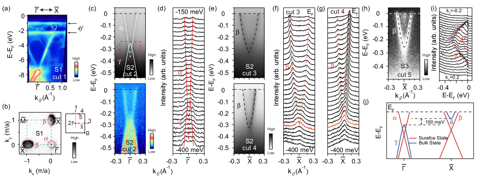
Figure 1(a) shows the photoemission intensity of YbB6 on sample 1 (S1) over a large energy scale, the non-dispersive Yb 4 bands are located at around 1 eV and 2.3 eV below Fermi energy () . They correspond to the 6H5/2 and 6H7/2 multiplets of the Yb2+ 46-45 final states based on the LDA calculation Ybcalc . The energy difference between the two multiplets is 1.3 eV, consistent with the calculation. However, the energy positions of these 4 bands are deeper than that calculated in Ref. Ybcalc, , probably due to the chemical potential shift induced by carrier doping. In addition, the dispersive feature centered at between the two 4 bands should originate from the Yb 5 band.
The photoemission intensity map at on S1 is shown in Fig. 1(b). An elliptical Fermi pocket located around and a circular Fermi pocket around are clearly observed. The photoemission intensity distribution across taken on sample 2 (S2) is plotted in Fig. 1(c), together with a background-substracted one to visualize the dispersions more clearly. There is an electron-like band (referred to as ), forming the circular Fermi pocket in Fig. 1(b). In Fig. 1(e), another electron-like band is observed around (referred to as ), forming the elliptical Fermi pocket.
Both the and bands exhibit almost linear dispersions as can be seen from their momentum distribution curves (MDCs) in Figs. 1(d), 1(f) and 1(g). The band extrapolates to cross at about 380 meV below . There is also a band below the band. However, the band bottom of overlaps with the band top of in certain energy range as highlighted in Fig. 1(c). This observation, together with the very different intensities of and , indicates that is not the lower cone of , if there is a Dirac point as predicted Ybcalc . Due to the low intensity of the band and the interference of the strong band, the lower cone is hardly resolved, if any.
The band also seems to cross at about 320 meV below by tracking its linear dispersion, but the predicted lower cone could not be distinguished either, due to the strong residual intensity of the flat 4 bands. The band is observed with a different photon energy on sample 3 (S3) with its band bottom around -80 meV [Fig. 1(h)]. The band bottom of in S3 is around -250 meV, different from that in S2, which may be caused by different chemical potentials. Figure 1(j) is the schematic of all the low-lying energy bands resolved along - direction.

Photon energy dependent ARPES experiments have been performed to examine how the , and bands vary with . The photoemission intensity distributions taken with different photon energies are presented in Fig. 2. One can see that, for both and bands, although the spectral weight varies with photon energy due to photoemission matrix element effects, the dispersions of them remain unchanged. Figures 2 (a) and 2(b) show the photoemission intensity distributions across on sample 4 (S4) together with their corresponding MDCs. We fitted the dispersion of the band taken with 94 eV photons and overlaid it onto the data taken with several other photon energies, which clearly show that the dispersions of the band are independent. The same process has been done to the band in Figs. 2(c) and 2(d), which also show no dependence of the band. More data under other photon energies can be found in the SM. Furthermore, the - intensity plot at shown in Fig. 2(g) demonstrates the two-dimensional nature of the and bands.
However, in Figs. 2(e) and 2(f), when we overlaid the dispersion of extracted from the MDCs taken with 103 eV photons on top of data taken with several other photon energies, there are clear mismatches. That is, the band disperses with , indicative of its bulk origin. Furthermore, the dark interior of intensity envelopes of the band in Fig. 2(e) is likely due to its dispersion along and the poor resolution in ARPES measurements with vacuum ultraviolet photons. Similar behavior has been reported for a bulk band in SmB6 JJSmB6 .
In addition, the band is only observed in certain photon energies, due to different cross-section of this band. The lineshape of the band is hardly resolved due to its bulk origin and poor resolution, which result in a bright interior of intensity envelopes of the band. Thus the band should be the bulk conduction band. As the band bottom of the band in S3 is around -80 meV, the band bottom of in S2 should be around -150 meV, due to different chemical potential between these two samples (see SM). Moreover, since the band top in the 91 eV data of S2 locates at around -250 meV [Fig. 1(c)], the bulk band gap of YbB6 is likely to be about 100 meV, as illustrated in Fig. 1(j). This determined gap size is much larger than the theoretical prediction of only 31 meV Ybcalc , which suggests the correlation effect needs to be better treated.
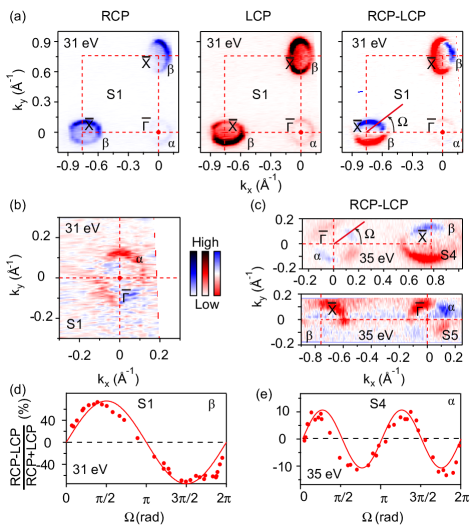
The chirality of spin and orbital angular momentum (OAM) is another remarkable hallmark of the topological surface state, since both of them are interlocked and rotate with the electron momentum, so that the total angular momentum is conserved. To further explore the topological nature of these surface states, we conducted CD-ARPES experiment, which probes the chirality of the OAM.Changyoung ; JJSmB6

The Fermi surface maps of S1 measured under right-handed circular polarized (RCP) light and left-handed circular polarized (LCP) light are shown in Fig. 3(a), together with their difference (referred to as RCP-LCP). The CD of the pocket shows an anti-symmetric pattern about the - axis in the surface BZ. The enlarged CD image near is shown in Fig. 3(b). Although its intensity is much weaker than that of the pocket, we can see that the symmetry of the pocket becomes two-fold, which is different from the anti-symmetric CD pattern of the pocket. Such symmetries are confirmed by another set of data with more statistics in the top panel of Fig. 3(c), which was measured on S4 at a different photon energy. The bottom panel in Fig. 3(c) is measured on sample 5 (S5), under the same condition as S2, but presents the left pocket. Clearly, all the CD patterns exhibit an inversion symmetry with respect to . Moreover, there is a sign change between the 31 eV and 35 eV CD data in both the and pockets. The simultaneous sign change can be attributed to a final-state effect of the CD-ARPES as reported in Bi2Se3 BiTeCD . In Figs. 3(d) and 3(e), we plot the representative CD distributions around the and pockets. Both of them can be well fitted by a sine function, however, the period for is 2, and that for is . The reductive period of the band, or the two-fold symmetric CD pattern needs further investigation, but similar behaviors were attributed to the coupling to bulk states in Bi2Se3 and Bi2Te3 Jung ; Bahramy ; CD_theory ; YHWang_2 . Despite the complexity, the CD results do suggest that the chirality of OAM exist in both the and bands, indicating that they might possess helical spin textures, further support their topological origin.

Having established the surface nature and the possible topological origin of the and bands, we briefly discuss the Z2 topology that can be determined from these bands. Since we observed one Fermi pocket around and two Fermi pockets around in the surface BZ, the total number of surface states is odd, thus the whole system should be topologically non-trivial. This is remarkably consistent with the theoretical prediction that YbB6 is a TI Ybcalc .
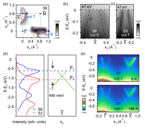
For a surface state, the work function depends directly on the surface conditions. In various cleavages, we observed that the work function of YbB6 varies about 100 meV, exposing the electronic structures discussed above. However, we observed a hole-like pocket around twice, referred to as in Figs. 4(a)-4(c). Sometimes, the electron-like Fermi pocket and the hole-like Fermi pocket can even be observed in different regions of the same sample, which requires further elucidation by scanning tunneling microscopy. The linear extrapolation of the band leads to a crossing at around 180 meV above . The slope of near its crossing point, and the observed slope of only differs about 4 %, therefore should be the lower half of the Dirac cone of . Since the Dirac point of is located at around 320 meV below , the shift of the chemical potential is about 500 meV, which equally affects the 4 band as shown in Fig. 4(d). On the other hand, due to the weak intensity of the band, we did not resolve its lower cone.
The observed surface states in YbB6 is robust against the change of temperature from 6 K to 196 K [Fig. 4(e)]. This is consistent with the DFT calculations which show that YbB6 is not a topological Kondo insulator Ybcalc .
To summarize, we have obtained a comprehensive understanding of the electronic structure of YbB6 from ARPES. We directly observed several linearly dispersive bands within the insulating gap of YbB6 which show negligible dependence. The CD-ARPES data suggest well-defined helical spin texture of the surface states. These results suggest that YbB6 is a TI. In addition, the insulating gap observed here is much larger than that reported in theoretical calculations, indicating correlation effects. We note that the sensitivity of work function reported here also implies its tunability. If the work function can be tuned into the 100 meV insulating gap, the topological surface state can be exploited in applications without the interference from the bulk states.
We thank Dr. Ming Shi and Dr. N. Xu at SLS and Dr. K. Ono and Dr. N. Inami at KEK. This work is supported in part by the National Science Foundation of China and National Basic Research Program of China (973 Program) under the grant Nos. 2012CB921402, 2011CB921802, 2011CBA00112. SSRL is operated by the U. S. DOE Office of Basic Energy Science.
References
- (1) Y. Kato et al., Journal of Crystal Growth 330, 39-42 (2011)
- (2) A. Menth, E. Buehler, H.J. Levinstein, T.H. Geballe, J. Appl. Phys. 40, 1006 (1969).
- (3) M. I. Ignatov, A. V. Bogach, G. S. Burkhanov, V. V. Glushkov, S. V. Demishev, A. V. Kuznetsov, O. D. Chistyakov, N. Y. Shitsevalova, N. E. Sluchanko, J. Exp. Theor. Phys. 105, 58 (2007).
- (4) Y. Mori, N. Shino, S. Imada, S. Suga, T. Nanba, M. Tomikawa, S. Kunii, Physica B 66, 86-188 (1993).
- (5) S. Souma, H. Komatsu, T. Takahashi, R. Kaji, T. Sasaki, Y. Yokoo, J. Akimitsu, Phys. Rev. Lett. 90, 027202-1 (2003).
- (6) Z. Fisk, P. H. Schmidt, L. D. Longinotti, Mater. Res. Bull. 11, 1019 (1976).
- (7) D. J. Kim, T. Grant, and Z. Fisk, Phys. Rev. Lett. 109, 096601 (2012).
- (8) D. J. Late, K. S. Date, M. A. More, P. Misra, B. N. Singh, L. M. Kukreja, C. V. Dharmadnikari, D. S. Joag, Nanotechnology 19, 265605 (2008).
- (9) S. Massidda et al., Z. Phys. B 102, 83-89 (1997).
- (10) M. Dzero et al., Phys. Rev. Lett. 104, 106408 (2010).
- (11) J. Jiang et al., Nat. Commun. 4, 3010 (2013).
- (12) M. Neupane et al., Nat. Commun. 4, 2991 (2013).
- (13) E. Frantzeskakis et al., Phys. Rev. X 3, 041024 (2013).
- (14) A. Aprea et al., Solid State Sciences 21, 32-36 (2013).
- (15) Hongming Weng, Jianzhou Zhao, Zhijun Wang, Zhong Fang, and Xi Dai, Phys. Rev. Lett. 112, 016403 (2014).
- (16) B. A. Bernevig, T. L. Hughes, and S. C. Zhang, Science 314, 1757 (2006).
- (17) M. Konig, S. Wiedmann, C. Brune, A. Roth, H. Buhmann, L. W. Molenkamp, X.-L. Qi, and S.-C. Zhang, Science 318, 766 (2007).
- (18) H. Zhang, C.-X. Liu, X.-L. Qi, X. Dai, Z. Fang, and S.-C. Zhang, Nat. Phys. 5, 438 (2009).
- (19) Y. Xia, D. Qian, D. Hsieh, L. Wray, A. Pal, H. Lin, A. Bansil, D. Grauer, Y. S. Hor, R. J. Cava, et al., Nat. Phys. 5, 398 (2009).
- (20) Y. L. Chen, J. G. Analytis, J. H. Chu, Z. K. Liu, S. K. Mo, X. L. Qi, H. J. Zhang, D. H. Lu, X. Dai, Z. Fang, et al., Science 325, 178 (2009).
- (21) J. M. Tarascon, J. Etourneau, P. Dordor, P. Hagenmuller, M. Kasaya, and J. M. D. Coey, J. Appl. Phys. 51, 574 (1980).
- (22) Y. L. Chen et al., Science 325, 178 (2009).
- (23) D. Hsieh et al., Nature 460, 1101 (2009).
- (24) M. R. Scholz et al., Phys. Rev. Lett. 110, 216801 (2013).
- (25) Y. H. Wang et al., Phys. Rev. Lett. 107, 207602 (2011).
- (26) Z. H. Zhu et al., Phys. Rev. Lett. 110, 216401 (2013).
- (27) C-H. Park, and Steven G. Louie, Phys. Rev. Lett. 109, 097601 (2012).
- (28) S. R. Park et al., Phys. Rev. Lett. 108, 046805 (2012).
- (29) Y. H. Wang and Nuh Gedik, Phys. Status Solidi RRL 7, No. 1-2, 64-71 (2013).
- (30) H. Mirhosseini and J. Henk, Phys. Rev. Lett. 109, 036803 (2012).
- (31) W. Jung et al., Phys. Rev. B 84, 245435 (2011).
- (32) M. S. Bahramy et al., Nature Communications 3, 1159 (2012).