Electrically Tunable Quasi-Flat Bands, Conductance and Field Effect Transistor in Phosphorene
Abstract
Phosphorene, a honeycomb structure of black phosphorus, was isolated recently. We investigate electric properties of phosphorene nanoribbons based on the tight-binding model. A prominent feature is the presence of quasi-flat edge bands entirely detached from the bulk band. We explore the mechanism of the emergence of the quasi-flat bands analytically and numerically from the flat bands well known in graphene by a continuous deformation of a honeycomb lattice. The quasi-flat bands can be controlled by applying in-plane electric field perpendicular to the ribbon direction. The conductance is switched off above a critical electric field, which acts as a field-effect transistor. The critical electric field is anti-proportional to the width of a nanoribbon. This results will pave a way toward nanoelectronics based on phosphorene.
Graphene is one of the most fascinating material found in this decadeNetoRev ; KatsText . The low-energy theory is described by massless Dirac fermions, which leads to various remarkable electrical properties. In practical applications to current semiconductor technology, however, we need a finite band gap in which electrons cannot exist freely. For instance, armchair graphene nanoribbons have a finite gap depending on the widthFujita ; EzawaRibbon , while bilayer graphene under perpendicular electric field also has a gapBilayer . It is desirable to find an atomic monolayer bulk sample which has a finite gap. Silicene is one of the promising candidates of post graphene materials, which is predicted to be a quantum spin-Hall insulatorLiuPRL . A striking property of silicene is that a topological phase transition is induced by applying electric fieldEzawaNJP . Nevertheless, silicene has so far been synthesized only on metallic surfacesGLay ; Takamura ; Kawai . Another promising candidate is a transition metal dichalcogenides such as molybdeniteMak ; Zeng ; Cao .
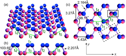
A new comer challenges the race of the post-graphene materials. That is phosphorene, a honeycomb structure of phosphorus. It has been successfully obtained in the laboratoryLi ; Liu ; Xia ; Gomez ; Koenig and revealed a great potential in applications to electronics. Black phosphorus is a layered material where individual atomic layers are stacked together by Van der Waals interactions. Just as graphene can be isolated by peeling graphite, phosphorene can be similarly isolated from black phosphorus by the mechanical exfoliation method. As a key structure it is not planer but puckered due to the hybridization, as shown in Fig.1. There are already several works based on first-principle calculationsPeng ; Tran ; Qiao ; Fei . The tight-binding model was proposedKats only recently by including the transfer energy over the 5 neighbor hopping sites (), as illustrated in Fig.1.
The aim of this paper is to investigate the physics of phosphorene nanoribbons based on the tight-binding model. The tight-binding model is essential to make a deeper understanding of the system, which is not attained by first-principle calculations and low-energy effective theory. Aa a striking property of phosphorene nanoribbon, we demonstrate the presence of a quasi-flat edge band which is entirely detached from the bulk band. We explore the band structure of phosphorene nanoribbon numerically and analytically from that of graphene nanoribbon as a continuous deformation of the honeycomb lattice by changing the transfer energy parameters . The graphene is well explained in terms of electron hopping between the first neighbor sites with and , where the presence of flat bands is well knownFujita ; EzawaRibbon . We follow the fate of the flat bands by changing these parameters. The essential roles is played by the ratio : The flat bands are detached from the bulk band when the ratio is , while the flat bands are bent by the term .
It is an exciting problem to control the band structure externally. We may change the band gap by applying external electric field perpendicular to the phosphorene sheet with the use of the puckered structure. Although we can control the band gap, the amount of the controlled gap is very tiny compared to the large band gap, that is, eV since the height of the puckered structure is the order of nm. On the other hand, the quasi-flat edge band is found to be sensible to external electric field parallel to the phosphorene sheet. This is because a large potential difference () is possible between the two edges if the width of the nanoribbon is large enough. We propose a field-effect transistor driven by in-plane electric field with the use of the quasi-flat edge bands. The conductance is shown to be either or with respect to the in-plane electric field. If the nanoribbon width is , the critical electric field is given by meV/nm. This is experimentally feasible.
.1 4-band tight-binding model.
The unit cell of phosphorene contains 4 phosphorus atoms, where two phosphorus exist in the upper layer and the other two phosphorus exist in the lower layer. The tight-binding model of phosphorene was recently proposedKats and is given by
| (1) |
where summation runs over the lattice sites, is the transfer energy between th and th sites, and () is the creation (annihilation) operator of electrons at site (). It has been shown that it is enough to take hopping links, as illustrated in Fig.1. The transfer energy explicitly reads as eV, eV, eV, eV, eV for these links.
In the momentum representation the 4-band Hamiltonian reads as with
| (2) |
where
| (3) |
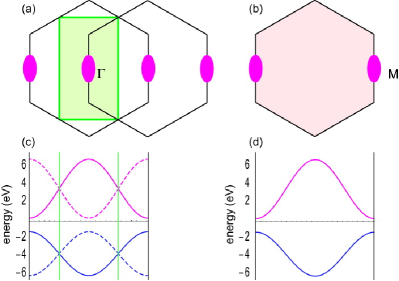
We show the Brillouin zone and the energy spectrum of the tight-binding model in Fig.2(a) and (c), respectively.
.2 2-band tight-binding model.
We are able to reduce the 4-band model to the 2-band model due to the point group invariance. We focus on a blue point (atom in upper layer) and view other lattice points in the crystal structure (Fig.1). We also focus on a red point (atom in lower layer) and view other lattice points. As far as the transfer energy is concerned, the two views are identical. Namely, we may ignore the color of each point. Hence, instead of the unit cell containing 4 points, it is enough to consider the unit cell containing only 2 points. This reduction makes our analytical study considerably simple.
The 2-band model is given by with
| (4) |
The rectangular Brillouin zone of the 4-band model is constructed by folding the hexagonal Brillouin zone of the 2-band model, as illustrated in Fig.2(a).
The equivalence between the two models (2) and (4) is verified as follows. We have explicitly shown the energy spectra of the 4-band model (2) and the 2-band model (4) in Fig.2(c) and (d), respectively. It is demonstrated that the energy spectrum of the 4-band model is constructed from that of the 2-band model: The two bands are precisely common between the two models, while the extra two bands in the 4-band model are obtained simply by shifting the two bands of the 2-band model, as dictated by the folding of the Brillouin zone.
.3 Phosphorene nanoribbons.
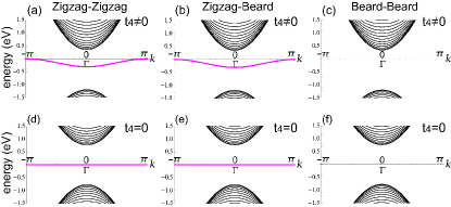
We investigate the band structure of a phosphorene nanoribbon placed along the direction (Fig.1). We study zigzag and beard edges. There are three types of nanoribbons, whose edges are (a) both zigzag, (b) zigzag and beard, (c) both beard. We show their band structures in Fig.3(a), (b) and (c), respectively.
A prominent feature is the presence of the edge modes isolated from the bulk modes found in Fig.3(a) and (b). They comprise a quasi-flat band. It is doubly degenerate for a zigzag-zigzag nanoribbon, and nondegenerate for a zigzag-beard nanoribbon, while it is absent in a beard-beard nanoribbon [Fig.3(c)].
Let us explore the mechanism how such an isolated quasi-flat band appears in phosphorene. By diagonalizing the Hamiltonian, the energy spectrum reads
| (5) |
The band gap is given by
| (6) |
The asymmetry between the positive and negative energies arises from the term. Then it is interesting to see what would happen when we set . We show the band structures in Fig.3(d), (e) and (f) for the three types of nanoribbons, where the quasi-flat edge modes are found to become perfectly flat. Consequently it is enough to show the emergence of the flat band by studying the model with . Furthermore it is a good approximation to set , since the transfer energies and are much larger than the others. Indeed we have checked numerically that no qualitative difference is induced by this approximation.
.4 Flat bands in anisotropic honeycomb lattice.
To explore the origin of the isolated quasi-flat band we analyze the anisotropic honeycomb-lattice model, which is described by the Hamiltonian (4) by setting . This Hamiltonian is well studied in the context of graphene and optical latticePereira ; Monta ; Wunsch ; Tar . The energy spectrum reads
| (7) |
which implies the existence of two Dirac cones at
| (8) |
for .
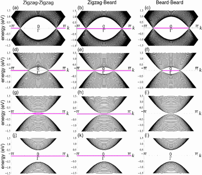
We now study the change of the band structure of nanoribbon by a continuous deformation of the honeycomb lattice, starting that of graphene. We show the band structure with (a) the zigzag-zigzag edges, (b) the zigzag-beard edges, and (c) the beard-beard edges in Fig.4 for typical values of and .
(i) We start with the isotropic case , where the energy spectrum (7) becomes that of graphene with two Dirac cones at the and points. The perfect flat band connects the and points, that is, it lies for (a) and ; (b) ; (c) . It is attached to the bulk band. See Fig.4(a),(b),(c). The topological origin of flat bands in graphene has been thoroughly discussedHatsugai .
(ii) As we increase but keeping fixed, the two Dirac points move towards the point (), as is clear from (8). The flat band keeps to be present between the two Dirac points. See Fig.4(d),(e),(f).
(iii) At , the two Dirac points merge into one Dirac point at the point, as implied by (8). The flat band touches the bulk band at the point for the zigzag-zigzag nanoribbon and the zigzag-beard nanoribbon, but disappears from the beard-beard nanoribbon. See Fig.4(g),(h),(i).
(iv) For , the bulk band shifts away from the Fermi level, as follows from (7). The flat band is disconnected from the bulk band for the zigzag-zigzag nanoribbon and the zigzag-beard nanoribbon, where it extends over all region . On the other hand, the edge band becomes a part of the bulk band and disappears from the Fermi level for the beard-beard nanoribbon. See Fig.4(j),(k),(l).
.5 Energy spectrum of quasi-flat bands.
We have explained how the flat band appears in the anisotropic honeycomb-lattice model. The flat band is bent into the quasi-flat band by switching on the transfer interaction .
We can derive the energy spectrum of the quasi-flat band perturbatively. We construct an analytic form of the wave function at the zero-energy state in the anisotropic honeycomb-lattice model (). By solving the Hamiltonian matrix recursively from the outer most cite, we obtain the analytic form of the local density of states of the wave function for odd cite ,
| (9) |
with . The wave function is zero for even cite. It is perfectly localized at the outer most cite when , and describes the flat band. With the use of this wave function, the energy spectrum of the quasi-flat band is estimated perturbatively by taking the expectation value of the term as
| (10) |
where . On the other hand we numerically obtain eV. The agreement is excellent.
.6 Phosphorene nanoribbons with in-plane electric field.
It is an intriguing problem to control the band structure externally. We may try to change the band gap by applying external electric field perpendicular to the phosphorene sheet. We find the band gap to behave as
| (11) |
where is the separation between the upper and lower layers. The gap becomes simply larger when we apply . Furthermore, in practical applications, it needs very large electric field since is the order of nm.
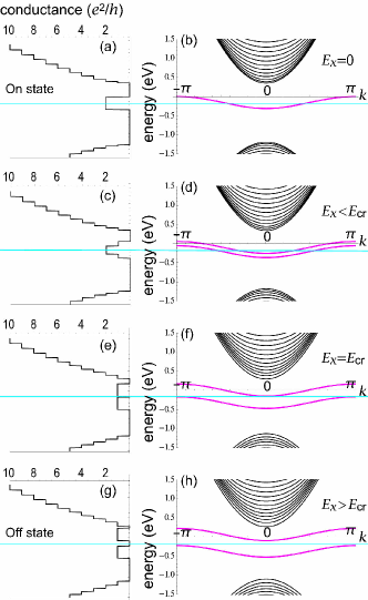
On the other hand, it is possible to make a significant change of the quasi-flat edge band by applying external electric field parallel to the phosphorene sheet. Let us apply electric field into the direction of a nanoribbon with zigzag-zigzag edges. A large potential difference () is possible between the two edges if the width of the nanoribbon is large enough. This potential difference resolves the degeneracy of the two edge modes, shifting one edge mode upwardly and the other downwardly without changing their shapes. We present the resultant band structures in Fig.5 for typical values of .
.7 Field-effect transistor.
Electric current may flow along the edge. We show the conductance in Fig.5. Without in-plane electric field, the conductance at the Fermi energy is since there is a two-fold degenerate quasi-flat band. Above the critical electric field, the conductance becomes since the quasi-flat band splits perfectly. This acts as a field-effect transistor driven by in-plane electric field. The critical electric field is anti-proportional to the width .
We derive the critical electric field . The energy shift at is given by since the wave function is perfectly localized at the outer most edge cite. In general the energy shift is given by
| (12) |
It is well approximated by for wide nanoribbons. The conductance is written as
| (13) |
where is the step function for and for . The critical electric field is determined as
| (14) |
If the nanoribbon width is , the critical electric field is given by meV/nm. This is experimentally feasible.
.8 Discussion.
We have analyzed the band structure of phosphorene nanoribbons based on the tight-binding model, and demonstrated the presence of quasi-flat edge modes entirely detached from the bulk band. Starting from the well-known structure of graphene, we have explained the mechanism how such edge modes emerge by a continuous deformation of the honeycomb lattice. The conductance due to the quasi-flat edge modes is quantized to be either or with respect to the in-plane electric field . The critical electric field is meV/nm for a nanoribbon with width . A field-effect transistor is possible with the use of this property. We may also expect a similar structure made of arsenic and antimony, which should be called as "arsenene" and "antimonene". The electronic properties will be explained simply by setting the transfer energies appropriately.
.9 Acknowledgements
The author thanks the support by the Grants-in-Aid for Scientific Research from the Ministry of Education, Science, Sports and Culture No. 25400317. M. E. is very much grateful to N. Nagaosa for many helpful discussions on the subject.
Supporting Materials
.10 Wave function of edge state.
We construct an analytic form of the wave function at the zero-energy state in the anisotropic honeycomb-lattice model () as follows. We label the wave function of the atom on the outer most cite as , and that of the atom next to it as , and as so on. The total wave function is if there are atoms across the nanoribbon. The Hamiltonian is explicitly written as
| (15) |
with . The eigenvalue problem is trivially solved, yielding and .
.11 Electric field.
We apply electric field perpendicular to the sheet. It is necessary to use the 4-band tight-binding model, since the electric field breaks the point group invariance. Namely, the upper and lower layers are distinguished by the electric field. We introduce into the Hamiltonian (2),
| (18) |
By diagonalizing this Hamiltonian at , the band gap is found to be
| (19) |
which yields numerically (11) in the text.
.12 Low-energy theory.
In the vicinity of the point, we make a Tayler expansion and obtain
| (20) |
The Hamiltonian (4) reads
| (21) |
with the Pauli matrices , where
| (22) |
Hence the dispersion is linear in the direction but parabolic in the direction. The low-energy Hamiltonian agrees with the previous resultRodin with a rotation of the Pauli matrices and .
.13 Conductance.
In terms of single-particle Green’s functions, the low-bias conductance at the Fermi energy is given byDatta
| (23) |
where with the self-energies and , and
| (24) |
with the Hamiltonian for the device region. The self-energy describes the effect of the electrode on the electronic structure of the device, whose the real part results in a shift of the device levels whereas the imaginary part provides a life time. It is to be calculated numericallySancho ; Rojas ; Nikolic ; EzawaAPL . We have used this formula to derive the conductance in Fig.5.
References
- (1) Castro Neto, A. H. , Guinea, F., Peres, N. M. R., Novoselov, K. S. & Geim, A. K. The electronic properties of graphene. Rev. Mod. Phys. 81, 109 (2009).
- (2) M. I. Katsnelson, Graphene: Carbon in Two Dimensions (Cambridge Univ. Press, Cambridge, 2012).
- (3) Fujita, M. et al. Peculiar Localized State at Zigzag Graphite Edge. J. Phys. Soc. Jpn. 65, 1920 (1996).
- (4) Ezawa, M. Peculiar width dependence of the electronic properties of carbon nanoribbons. Phys. Rev. B 73, 045432 (2006).
- (5) McCann E. & Fal’ko, V. I. Landau-Level Degeneracy and Quantum Hall Effect in a Graphite Bilayer. Phys. Rev. Lett. 96 (2006) 086805.
- (6) Liu, C.-C., Feng, W. & Yao, Y. Quantum spin Hall effect in silicene and two-dimensional germanium. Phys. Rev. Lett. 107, 076802 (2011).
- (7) Ezawa, M. Topological Insulator and Helical Zero Mode in Silicene under Inhomogeneous Electric Field. New J. Phys. 14, 033003 (2012).
- (8) Vogt, P., De Padova, P., Quaresima, C., Frantzeskakis, E., Asensio, M. C., Resta, A., Ealet, B. & Lay, G. L. Silicene: Compelling Experimental Evidence for Graphenelike Two-Dimensional Silicon. Phys. Rev. Lett. 108, 155501 (2012).
- (9) Fleurence, A., Friedlein, R., Ozaki, T., Kawai, H., Wang, Y., & Yamada-Takamura, Y. Experimental Evidence for Epitaxial Silicene on Diboride Thin Films. Phys. Rev. Lett. 108, 245501 (2012).
- (10) Lin, C.-L., Arafune, R., Kawahara, K., Tsukahara, N., Minamitani, E., Kim, Y., Takagi, N. & Kawai, M. Structure of Silicene Grown on Ag (111), Appl. Phys. Express 5, 045802 (2012) .
- (11) Mak, K. F., Lee, C., Hone, J., Shan, J. & Heinz, T. F. Atomically Thin MoS2: A New Direct-Gap Semiconductor, Phys. Rev. Lett. 105, 136805 (2010)
- (12) Zeng, H., Dai, J., Yao, W., Xiao D. & Cui, X. Valley polarization in MoS2 monolayers by optical pumping. Nat. Nanotech. 7, 490 (2012).
- (13) Cao, T., Wang, G., Han, W., Ye, H., Zhu, C., Shi, J., Niu, Q., Tan, P., Wang, E., Liu, B. & Feng, J. Valley-selective circular dichroism of monolayer molybdenum disulphide. Nat. Com. 3, 887 (2012).
- (14) Li, L., Yu, Y., Ye, G. J., Ge, Q., Ou, X., Wu, H., Feng, D., Chen, X. H., Zhang, Y. Black phosphorus field-effect transistors. cond-mat/arXiv:1401.4117 :Nat. Nanotech (2014).
- (15) Liu, H., Neal, A. T., Zhu, Z., Xu, X., Tomanek, D. & Ye, P. D. Phosphorene: A New 2D Material with High Carrier Mobility. ACS Nano 8 4033 (2014)
- (16) Xia, F., Wang, H., & Jia, Y. Rediscovering Black Phosphorus: A Unique Anisotropic 2D Material for Optoelectronics and Electronics. cond-mat/arXiv:1402.0270
- (17) Castellanos-Gomez, A. et.al. Isolation and characterization of few-layer black phosphorus. cond-mat/arXiv:1403.0499
- (18) Qiao, J., Kong, X., Hu, Z.-X., Yang, F. & Ji, W. Few-layer black phosphorus: emerging 2D semiconductor with high anisotropic carrier mobility and linear dichroism. cond-mat/arXiv:1401.5045
- (19) Tran, V., Soklaski, R., Liang, Y., & Yang, L. Layer-Controlled Band Gap and Anisotropic Excitons in Phosphorene. cond-mat/arXiv:1402.4192
- (20) Koenig, S. P., Doganov, R. A., Schmidt, H., Castro Neto, A. H. & Oezyilmaz, B. Electric field effect in ultrathin black phosphorus. cond-mat/arXiv:1402.5718
- (21) Fei, R. & Yang, L. Strain-Engineering Anisotropic Electrical Conductance of Phosphorene and Few-Layer Black Phosphorus. cond-mat/arXiv:1403.1003
- (22) Peng, X., Copple, A. & Wei, Q. Strain engineered direct-indirect band gap transition and its mechanism in 2D phosphorene. cond-mat/arXiv:1403.3771
- (23) Rudenko N. & Katsnelson, M. I. Quasiparticle band structure and tight-binding model for single- and bilayer black phosphorus. cond-mat/arXiv:1404.0618
- (24) Pereira, V. M., Castro Neto, A. H. & Peres, N. M. R. Tight-binding approach to uniaxial strain in graphene. Phys. Rev. B 80, 045401 (2009).
- (25) Montambaux, G., Piechon, F., Fuchs, J. -N., et al. Merging of Dirac points in a two-dimensional crystal. Phys. Rev. B 80, 153412 (2009).
- (26) Wunsch, B., Guinea, F. & Sols, F. Dirac-point engineering and topological phase transitions in honeycomb optical lattices. New. J. Phys. 10, 103027 (2008)
- (27) Tarruell, L. et al. Creating, moving and merging Dirac points with a Fermi gas in a tunable honeycomb lattice. Nature 483, 7389 (2012).
- (28) Shinsei, R. & Hatsugai, Y. Topological Origin of Zero-Energy Edge States in Particle-Hole Symmetric Systems. Phys. Rev. Lett. 89, 077002 (2002).
- (29) Rodin, A. S., Carvalho, A. & Castro Neto, A. H. Strain-induced gap modification in black phosphorus. cond-mat/arXiv:1401.1801
- (30) Datta, S. Electronic Transport in Mesoscopic Systems. (Cambridge University Press, Cambridge, England, 1995): Quantum Transport: Atom to Transistor, (Cambridge University Press, England, 2005)
- (31) Sancho, M. P. L., Sancho, J. M. L. & Rubio, J. Highly convergent schemes for the calculation of bulk and surface Green functions. J. Phys. F: Met. Phys. 15, 851 (1985).
- (32) Muñoz-Rojas, F., Jacob, D. Fernández-Rossier, J. & Palacios, J. J. Coherent transport in graphene nanoconstrictions. Phys. Rev. B 74, 195417 (2006).
- (33) Zârbo, L. P. & Nikolić, B. K. Spatial distribution of local currents of massless Dirac fermions in quantum transport through graphene nanoribbons. EPL, 80 47001 (2007): Areshkin, D. A. & Nikolić, B. K. I-V curve signatures of nonequilibrium-driven band gap collapse in magnetically ordered zigzag graphene nanoribbon two-terminal devices. Phys. Rev. B 79, 205430 (2009).
- (34) Ezawa, M. Quantized conductance and field-effect topological quantum transistor in silicene nanoribbons. Appl. Phys. Lett. 102, 172103 (2013).