Is Silicene the Next Graphene?
Abstract
This article reviews silicene, a relatively new allotrope of silicon, which can also be viewed as the silicon version of graphene. Graphene is a two-dimensional material with unique electronic properties qualitatively different from those of standard semiconductors such as silicon. While many other two-dimensional materials are now being studied, our focus here is solely on silicene. We first discuss its synthesis and the challenges presented. Next, a survey of some of its physical properties is provided. Silicene shares many of the fascinating properties of graphene, such as the so-called Dirac electronic dispersion. The slightly different structure, however, leads to a few major differences compared to graphene, such as the ability to open a bandgap in the presence of an electric field or on a substrate, a key property for digital electronics applications. We conclude with a brief survey of some of the potential applications of silicene.
I Introduction
The study of nanomaterials took off some 40 years ago with the design of so-called quasi-two-dimensional (2D) (solids thin in one direction, typically around tens of nanometers or tens of atomic layers in thickness), quasi-one-dimensional (nanowires), and quasi-zero-dimensional solids (quantum dots). In 2004, the study of exact 2D solids became a renewed focus, as graphene was isolated from graphite, Novoselov2004a and its many fascinating properties were demonstrated. Graphite can be viewed as a stack of graphene sheets held together by the weak van der Waals bonding.
Graphene has a hexagonal arrangement of carbon atoms in two dimensions, with a very strong covalent bonding between them. One consequence is the extremely high mechanical strength of the graphene sheet. Another key consequence is that the electrons behave as if they are massless or relativistic electrons (so-called Dirac electrons), whereas electrons in standard semiconductors such as silicon behave as traditional electrons with mass; this has been shown to lead to electron mobilities a hundred times larger for graphene Bolotin2008a with the potential for much faster electronics than with conventional silicon (see the December 2012 special issue of MRS Bulletin on graphene). Furthermore, graphene is neither a semiconductor nor a metal, rather it is exactly in between and can be called a semimetal; technically, it is said to not have an electronic energy gap. The ease of making graphene by mechanical exfoliation (simply by peeling off graphene sheets from graphite using Scotch tape) and the demonstration of various properties of graphene led to Geim and Novoselov receiving the Nobel Prize in Physics in 2010.
A simple question after the discovery of graphene would be why not silicene (the silicon analog of graphene) or germanene (germanium analog) (i.e., the formation of 2D sheets from other atoms from group IV of the periodic table). Elements are grouped in the periodic table because of periodic trends in their physical and chemical properties, and thus carbon, silicon, germanium, tin, and lead are expected to have certain similar properties. A simple reason why the silicon analog of graphene was not immediately considered is related to the types of chemical bonding that are common for carbon and silicon. Carbon is known to form various types of covalent bonding (known as hybridization) involving two, three, and four electrons forming such materials as ethylene, graphite, and diamond, whereas silicon has been known to favor sharing four electrons equally, leading to bulk silicon. The key to making 2D silicon, however, is to take a broader view of two-dimensionality by not requiring all the atoms to form a flat sheet; for chemists, this means one is not strictly looking for the elusive bonding for silicon.
This broader understanding was already achieved at least as early as 1994 in a paper by Takeda and Shiraishi Takeda1994a in which they asked what kind of 2D structures of silicon and germanium might be possible. They carried out quantum mechanical ab initio calculations that represented the state of the art in predicting the properties of materials. They found that structures with minimum energies could be obtained if the two atoms in a unit cell (the smallest repeat unit needed to generate the whole infinite structure) are not in the same plane, leading to a sheet that has “dimples” rather than both atoms in the same plane as for graphene. In the process, they also obtained electronic energy curves revealing the semi-metallic property, but they did not know to look for the linear curves (so-called Dirac cones) indicative of the Dirac electrons. There was also some early work on making silicon nanosheets by chemical exfoliation and, in some cases, monolayers were reported, though they were also functionalized and in most cases not very stable. Nakano2005a ; Nakano2006a
The demonstration of the presence of Dirac cones in silicene first occurred in a paper published in 2007 by the authors of this article. Guzman-Verri2007a While previous papers had used a numerical method for computing the electronic energies, this study used an analytical model that was able to prove, independent of whether the 2D sheet is flat or dimpled, Dirac cones will result. This is also believed to be the first instance of the use of the word “silicene” to describe the silicon analog of graphene.
All of this previous work remained fairly obscure until , when a French group provided the first hints of the possible fabrication of silicene nanoribbons on a silver substrate. Kara2009a Activity since has grown exponentially, and silicene is now recognized as a promising 2D material beyond graphene.
II Growth of silicene
Since a graphite-like form of silicene does not exist and all the covalent bonds in bulk Si are equally strong, it is unlikely that a mechanical exfoliation technique could be developed for silicene. Hence, other techniques are needed. Two have been reported to date.
II.1 Wet chemistry method
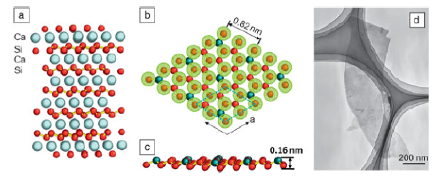
The first attempt at making an atomic layer of silicon was via chemical exfoliation of calcium disilicide Nakano2005a ; Nakano2006a (Figure 1). Chemical exfoliation is an attractive fabrication technique for nanostructures since it is a relatively inexpensive and low-technology technique. The basic idea is to use foreign atoms or ions to assist in splitting bonds (primarily via steric and kinetic attacks), leading to free layers. This, therefore, requires that the starting material have a layered structure (i.e., certain weaker bonds that can be preferentially broken while preserving other bonds within the layers). Thus, this technique is very effective for making graphene from graphite due to the weak interlayer van der Waals bonds. One common side effect of chemical exfoliation is a resulting functionalization of the prepared materials, particularly from the foreign atoms. However, if functionalization is desired, then this is an added advantage.
A number of possible candidates exist for making silicene via chemical exfoliation. Thus, calcium disilicide (CaSi2) has been used to prepare siloxene (a flat form of silicon with attached OH groups), which can then be exfoliated to produce siloxene nanosheets, Nakano2005a a form of functionalized silicene. Mg-doped silicene sheets capped with oxygen were obtained when Mg-doped CaSi2 was directly exfoliated using propylamine hydrochloride; Mg doping was used because the doping reduced the charges on the Ca and Si and, therefore, aided in the exfoliation. On the other hand, polysilane could be exfoliated in an organic solvent to give silicon nanosheets covered with organic groups instead of oxygen. Okamoto2010a ; Sugiyama2010a
II.2 UHV deposition
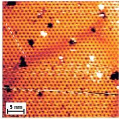
The first breakthrough in experimental silicene research was the report of the fabrication of silicene nanoribbons on a silver substrate oriented in the () direction. The technique used was an ultrahigh vacuum (UHV) deposition of silicon atoms onto a metallic substrate. Deposition is one approach to prevent 3D island formation, as bulk Si is more stable than silicene by eV/atom. Zhang2012a Currently, successful fabrication of silicene sheets has been reported using an Ag () substrate held at C and a slow deposition rate of Si below monolayer per minute Vogt2012a ; Lin2012a ; Feng2012a ; Chiappe2012a (Figure 2). Silver has turned out to be an ideal substrate because of the low reactivity between Si and Ag and because of the compatibility of the crystal structures and lattice constants.
There are still many unanswered questions about the growth of silicene on Ag. Thus, different superstructures of silicene on Ag have been reported, whether at one substrate temperature or at different temperatures, Lin2012a ; Jamgotchian2012a and there is not yet a conclusive explanation for all of these results. There appears to be a correlation with substrate temperature; Jamgotchian2012a however, theoretical modeling of structures (e.g., using molecular dynamics) is not at the level of predicting the superstructures. Two other results still under dispute concern the level of interaction between Si and Ag electronic states, and the presence or not of the Dirac electrons in silicene. These are related questions since they both concern what happens to the electrons in silicene in the presence of the Ag substrate; we will discuss this further later in the article. Silicene has also been reported to have been grown on ZrB2 Fleurence2012a and Ir (). Meng2013a
III Properties of silicene
III.1 Structure
Freestanding silicene can be viewed as a 2D material. However, it is not completely flat, as is graphene. The most commonly reported structure has been with alternate Si atoms lying in planes that are separated from each other in the direction perpendicular to the planes by Å(Figure 3a).
Nevertheless, it makes sense to still refer to these planes as forming a buckled 2D sheet. In fact, such a sheet is very similar to the () plane of Si.
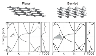
A hypothetical flat silicene has been shown to be metastable via calculation of the phonon modes. Cahangirov2009a The buckled form is also lower in energy by meV/atom Durgun2005a and has a binding energy of eV/atom, which is about eV/atom lower than for bulk Si. Cahangirov2009a More recent work now indicates that the honeycomb structure of Si might not be the lowest energy one; Kaltsas2013a rather, other slightly more stable structures were obtained by allowing the Si () plane to reconstruct. In fact, the other structures, the so-called and , (where the expressions label the geometrical commensurability with the basic unit cell) were found to be more stable than the silicene structure (Figure 3b-d). These examples were chosen because they are present in the surface reconstruction of bulk Si. Nevertheless, it is expected that the structure that is obtained in any given growth would be related to the growth conditions and substrate.
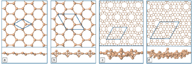
Thus, the structure of silicene on Ag is much more complex than previously thought, and a variety of superstructures have been reported from both experiments and theory. Vogt2012a ; Feng2012a ; Chiappe2012a ; Lalmi2010a ; Enriquez2012a ; Kaltsas2012a ; Gao2012a ; Arafune2013a ; Huang2013a Growth conditions, particularly substrate temperature, Huang2013a determine which superstructure is obtained. Some ambiguity remains due in part to experimental characterization (e.g., scanning tunneling micrfoscopy) not associating a unique and well-defined structure to a given image.
III.2 Elastic properties
Two-dimensional materials require a new definition of their elastic constants (e.g., the 3D bulk modulus is defined in terms of isotropic pressure and volume change). One could define in-plane stiffness,
| (1) |
in terms of the 3D elastic constants and , and an effective thickness . Sahin2009a One can also introduce 2D elastic constants via Wang2010a
| (2) |
where is the interlayer spacing of a hypothetical 3D supercell. Overall, it has been found that silicene is less rigid than graphene. This is easily understood in terms of the buckled structure of silicene compared to the flat structure of graphene.
With uniaxial strain, it is possible to open a bandgap, though the dependence has been found to be nonlinear. Zhao2012a The largest gap was found to be about meV for a strain of about %. Instability of the structure was obtained for a strain of %. On the other hand, a biaxial tensile strain converted silicene into a metallic state (for strain higher than %) due to the lowering of the conduction band at the point (the point in the Brillouin zone with zero wave vector). Liu2012a ; Qin2012a The latter result is different from graphene, which remains as a zero-gap material.
III.3 Electronic properties
The fascination with silicene is similar to that for graphene - freestanding silicene has been predicted to have Dirac cones just like graphene. It should be repeated that this result, at first sight, is not obvious due to the lower symmetry of silicene compared to graphene. Nevertheless, it has been shown rigorously that the degree of buckling does not affect the existence of the zero bandgap in the absence of spin-orbit coupling, from symmetry arguments. Guzman-Verri2007a A similar result derived from ab initio calculations is given in Figure 4.
Figure 5 depicts the so-called band structure, which is a plot of the electron energy versus its wave vector (related to its momentum). The point at the intersection of the Fermi level (which basically represents the separation between filled and unfilled electron states), given here at zero energy, and the point K shows the absence of the bandgap and the linear crossing of curves, the Dirac cone (when the line is rotated). The band structure can be recovered experimentally, with the most direct technique currently in use being the so-called ARPES (angle-resolved photoelectron spectroscopy) method. A photon of energy is used to eject an electron of wave vector ; thus, simultaneous measurements of the two quantities are possible.
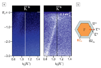
An example of an ARPES result is shown in Figure 5, which appears fairly convincing in showing a linear dispersion curve (the lighter region in the second panel on the left figure). Nevertheless, this result and another similar result Chen2012a have recently been questioned. Chen2013a ; Guo2013a ; Lin2013a ; Wang2013a Recent experiments have come to the conclusion that the linear dispersion actually becomes quadratic near the Dirac point. Arafune2013a Moreover, a search for massless Dirac electrons via the generation of the quantum Hall effect turned out negative. Lin2013a The latter experimental results have also received support from theoretical calculations, revealing a strong hybridization between the Si and Ag electronic states Lin2013a and also others attaching the linear dispersion to an band origination from the silver. Indeed, the linearity of the silicene electron is unlikely down to eV, as implied in Figure 5 (see the calculation of Wang and Cheng Wang2013a ). Still, defense of the Dirac cones persists, ranging from renewed identification of a linear tail to the silicene electronic dispersion even in the presence of a small gap Avila2013a to associating Dirac cones to only certain superstructures. Chen2013a Clearly, the study of silicene on silver remains complex and rich.
The electronic properties of silicene in the presence of a vertical electric field (i.e., perpendicular to the plane) are important for possible application as field-effect transistors. In contrast to graphene, a bandgap opens for silicene due to the lower symmetry of the buckled structure. In effect, the two atoms in the unit cell feel different electric potentials since they are at different heights. Two early calculations both obtained a fairly linear dependence of the gap on the electric field; Ni2012a ; Drummond2012a however, they obtained rates that differ by a factor of two.
It was noted previously that the bandgap is zero in the absence of spin–orbit coupling, which can split the bands and lead to a small gap opening. There are two contributions to the magnitude of the spin–orbit gap. One is the magnitude of the atomic spin–orbit coupling; the other relates to symmetry reduction due to buckling. It turns out that both effects contribute to a larger spin–orbit gap for silicene compared to graphene. It is, in fact, negligible for graphene, while it is about meV for silicene. Liu2011a While still small, it is sufficient to help demonstrate the quantum spin Hall effect; this effect arises from the existence of a bulk gapped state and gapless conducting edge states at the boundaries, an example of a topological insulator. An interesting proposal is to control the bandgap using an external electric field, Ezawa2012a ; Ezawa2012b ; Dyrdal2012a transforming silicene from a topological insulator into a band insulator. Indeed, silicene has been predicted to have an extremely rich phase diagram of topological states with unique quantum states of matter such as a hybrid quantum Hall-quantum anomalous Hall state (the anomalous effect being the well-known quantum Hall effect in the absence of an external magnetic field) and a so-called valley-polarized metal (resulting from electron transfer from a conduction valley to a different hole valley), leading to the new field of spin valleytronics. Ezawa2012c ; Ezawa2013a ; Tabert2013a
III.4 Optical
In any study of silicon-based materials, optical properties are an area of interest since one of the “holy grails” of materials science is silicon-integrated photonics. Bulk Si is known to be a poor light emitter due to its indirect bandgap. There have been few studies on the optical properties of silicene to date due in part to the zero gap for the freestanding sheet and to the increased difficulty in computing optical properties using density functional theory (DFT). The latter is known to be deficient in computing excited-state properties, necessary to describe optical properties. Furthermore, the semi-metallic nature of gapless silicene reduces the possible contribution due to electron screening, complicating the theory, particularly for single-particle ones. Experimentally, no results have yet been reported, due to the difficulty in peeling silicene from the Ag substrate.
Early calculations on hydrogenated silicon nanosheets (the effect of hydrogenation on the electronic properties is covered in more detail in the next section) of different orientations have revealed the possibility of obtaining direct energy gaps of the order of eV. Lu2009a We note, however, that detailed structures of the nanosheets were not provided, and they appear to be flat rather than buckled as we understand them to be now. Furthermore, those calculations were done using the generalized gradient approximation to DFT, which is known to underestimate the bandgap. Calculations that fix the previous problems Pulci2012a show that there can be a blueshift of the transition by about eV upon exciton formation and also an enhanced fundamental oscillator strength, which is about times stronger than for graphane (the hydrogenated form of graphene); the latter has been attributed to the different nature of the lowest conduction states (being mostly localized on silicon atoms for silicane (the hydrogenated form of silicene) and mostly on hydrogen atoms for graphane).
One would expect the infrared properties to be very similar to those of graphene since those are due to the zero gap, linear energy dispersion, and the 2D nature. Indeed, the universality of the optical absorption (proportional to the universal fine structure constant) based upon a single-particle picture has been predicted. Bechstedt2012a
Another aspect missing from the above is a study of excitons (the collective behavior of electrons and holes in optically excited materials) in silicene. It should be pointed out that even the excitonic spectrum of graphene is not fully understood. Recent calculations Wei2013a indicate that silicene also has resonant excitons like graphene.
III.5 Functionalization
In spite of the interest in pure silicene, there are a number of reasons why functionalization is of some importance. First and foremost, growth processes might naturally lead to functionalized sheets (e.g., via wet chemical methods). Second, the additional functionality introduced by adding various other atoms enlarges the variety of properties attainable. Four general types of functionalizations have been studied for silicene: hydrogenation, halogenation, by metals, and by organic groups.
Hydrogenation is, by far, the most studied. Lu2009a ; LewYanVoon2010a ; Garcia2011a ; Houssa2011a ; Jose2011a ; Ding2012a Hydrogenation of graphene was studied early on as a way of opening an energy gap; hence, it is natural to consider it for silicene as well. Also, experimentally, it is often possible to obtain hydrogenated samples. Theoretically, incorporation of hydrogen atoms is the standard approach to saturating dangling bonds. Finally, from an application perspective, one can also envision hydrogen storage as an important goal of silicon (and other material) research. The basic results are that full hydrogenation, with the resulting material being called silicane, does lead to a bandgap opening. LewYanVoon2010a Boat-like and chair-like configurations are found to be the most stable ones but with very different bandgaps ( eV direct and eV indirect, respectively, using many-body perturbation theory Houssa2011a ). More interestingly, half-hydrogenation is found to lead to a direct-gap insulator with a gap of eV for the chair configuration and a ferromagnetic state. Wang2012a ; Zhang2012b The latter has been attributed to the unpaired 3p electrons on the unhydrogenated silicon sites. On the basis of mean-field approximation arguments, the Curie temperature was estimated to be K. Wang2012a ; Zhang2012b One approach to obtaining half-hydrogenation is to first fully hydrogenate silicene and then apply a vertical electric field. Gang2013a
Fluorination performs a similar function as hydrogenation. It has been found that fluorinated silicene is more stable than silicane and with a smaller bandgap. Garcia2011a ; Ding2012a Bromine was found to lead to even more interesting behavior. Zheng2012a Half-brominated silicene is an antiferromagnetic half-metal, whereby one spin channel is metallic, and the other is semiconducting with a eV energy gap.
Metal adatoms display various states and properties, as one can expect from their variety. Even for graphene, metal adatoms have led to a variety of behaviors such as superconductivity with lithium and catalytic properties with transition metals. We refer the reader to the paper by Lin and Ni for an extensive study. Lin2012b A general conclusion is that metal adatoms bind much more strongly to silicene than to graphene. The bonding is covalent in all cases except for alkali metal atoms.
III.6 Other properties
In addition to the previous extensive studies, we would like to mention some other work on the properties of silicene. A few papers have been published on various thermal properties. Li2012a ; Hu2013a In particular, the in-plane thermal conductivity of silicene is found to be about an order of magnitude lower than for bulk Si. Vacancy defects lead to further reduction due to phonon-defect scattering. Furthermore, the thermal conductivity of silicene is found to initially increase with tensile strain, Hu2013a opposite to what is observed for graphene. The different behavior was traced to the fact that all the vibrational modes for graphene softened with tensile strain, whereas this is true for the longitudinal and transverse modes for silicene but not for the flexural modes (perpendicular to the layer). The latter competition between phonon softening and stiffening for silicene leads to a nonmonotonic behavior of the thermal conductivity as a function of strain.
IV Silicene nanoribbon
Graphene nanoribbons garnered interest as a means of opening a bandgap in graphene through the quantum confinement effect. For silicene, it was also the case that the first reported fabrication was actually of the nanoribbons rather than of the sheet. Vogt2012a Indeed, from a growth point of view, nanoribbons were very attractive due to the high uniformity of single nanoribbons (1.6 nm in width) and of arrays of the nanoribbons. The nanoribbons were initially reported to be grown on Ag (110), though this has also now been achieved on Au (110). Tchalala2013a They were also observed to be much more stable to molecular oxygen that bulk Si. Padova2011a
The electronic properties of freestanding silicene nanoribbons are fairly straightforward. Thus, armchair silicene nanoribbons (ASiNR) were all found to be nonmagnetic Ding2009a but could be metals or semiconductors. The zigzag silicene nanoribbons (ZSiNR) were found to have an antiferromagnetic semiconducting ground state. Here, armchair and zigzag describe nanoribbons with two different shapes of edges. These results are the same as for graphene nanoribbons.
Very large values of magnetoresistance have been predicted in silicene nanoribbons using first-principle calculations. Kang2012a Silicene nanoribbons with zigzag configurations have ferromagnetic states at the edges. By attaching the ends of the nanoribbon to electrodes and applying parallel magnetic fields to them, the nanoribbon shows a parallel spin configuration along its length. By applying antiparallel magnetic fields, the nanoribbon shows an antiparallel spin configuration. Upon applying a bias field between the electrodes, a current flows from one electrode to the other, and it increases with the bias field in an approximate linear fashion for both the parallel and antiparallel configurations. The calculated current of the parallel configuration is, however, several orders of magnitude greater than that of the antiparallel configuration as a result of distinct selection rules between electronic states. The percent change in the resistance is huge (%), and it is comparable to that of graphene nanoribbons. Kim2008a
V Applications
Given the similarity of silicene to graphene, many of the same potential applications of graphene have been considered for silicene. Experimentally, one is still far from any device fabrication given that silicene growth is still in its infancy and much about its properties remains to be characterized. Hence, we only provide a very brief survey of some of the applications being envisioned for silicene.
The most obvious such potential application is in nanoelectronics as transistors. Graphene transistors have already been demonstrated. The advantages of silicene are that it is compatible with current silicon nanoelectronics, and one can more easily open a gap, whether through coupling with a substrate, strain, or simply by using a vertical electric field. Ni2012a ; Drummond2012a The latter is obviously attractive for field-effect transistors (FETs). One current obstacle is obtaining silicene on an insulator, though this is being actively pursued. Houssa2010a ; Liu2013a Notwithstanding, the per- formance of a silicene nanoribbon FET has been modeled. Li2012a It is found that short ASiNR FETs have large current on/off ratios of over , and the output characteristic exhibits a saturation current, an effect absent for graphene nanoribbons.
Silicene has been proposed as an ideal spintronics and valleytronics material. The spin–orbit interaction for silicene is predicted to be relatively large compared to that for graphene, simply because the atomic spin–orbit coupling is larger for silicon than for carbon. Liu2011a This opens up the possibility of spin and valley physics otherwise difficult to observe in graphene. Tahir2013a It has been predicted that an electric current of a definite spin and valley label could be isolated. Ezawa2013a ; Tabert2013a Since the valley struc- ture can be controlled by an electric field, this could lead to an electric-field controlled spin filter. Wang2012a ; Tsai2013a .
Recently, it has been suggested that silicene may be suitable for energy storage applications. Tritsaris2013a The energy density of Li-ion batteries depends on the specific charge capacity of the electrodes. Being of atomic thickness, silicene could serve as a high-capacity host for Li. First-principles calculations find that freestanding single-layer and double-layer silicene have binding energies of about eV per Li atom, which do not vary much with respect to Li content and have smaller diffusion barriers (eV) than those of bulk silicon and silicon nanowires. Binding energies of silicene with other alkali, alkali-earth metals, groups III and IV metals, and transition metals have been calculated and were found to be stronger than those with graphene. Lin2012a Electronic band structures of lithiated silicene have been studied by first-principles calculations and showed that upon complete lithiation, the band structure of silicene transformed from a zero-gap semiconductor to a eV bandgap semiconductor. Osborn2012a
VI Summary
Silicene has been touted as the next graphene since it is predicted to display the same linear electronic dispersion, yet one can more easily induce a bandgap opening due to the reduced crystal symmetry. Additionally, it is compatible with current silicon microelectronics. While its fabrication has now been reproducibly verified, this has so far only been achieved on metallic substrates, limiting its potential applications in field-effect transistors. Promising avenues for both theoretical and experimental work also include ways in which it differs from graphene. One such activity that has been researched theoretically is in spintronics, whereby both the much larger spin–orbit coupling of silicon as compared to diamond and the symmetry difference between silicene and graphene have been exploited to propose new physics and applications. An explosive growth in silicene research will likely depend on the materials community achieving a breakthrough in making silicene easily, abundantly, and on a variety of substrates.
VII Acknowledgments
Our early research on silicene was partially funded by the National Science Foundation. Writing of this article was facilitated by funds from The Citadel Foundation, the Traubert Endowed Funds, and the US Department of Energy, Office of Basic Energy Sciences under contract no. DE-AC02-06CH11357.
References
- (1) K.S. Novoselov, A.K. Geim, S.V. Morozov, D. Jiang, Y. Zhang, S.V. Dubonos, I.V. Grigorieva, A.A. Firsov, Science 306, 666 (2004).
- (2) K.I. Bolotin, K.J. Sikes, Z. Jiang, M. Klima, G. Fudenberg, J. Hone, P. Kim,H.L. Stormer, Solid State Commun. 146, 351 (2008).
- (3) K. Takeda, K. Shiraishi, Phys. Rev. B 50, 14916 (1994).
- (4) H. Nakano, M. Ishii, H. Nakamura, Chem. Commun. 23, 2945 (2005).
- (5) H. Nakano, T. Mitsuoka, M. Harada, K. Horibuchi, H. Nozaki, N. Takahashi, T. Nonaka, Y. Seno, H. Nakamura, Angew. Chem. 118, 6451 (2006).
- (6) G.G. Guzmán-Verri, L.C. Lew Yan Voon, Phys. Rev. B 76, 075131 (2007).
- (7) A. Kara, C. Léandri, M.E. Dávila, P. de Padova, B. Ealet, H. Oughaddou, B. Aufray, G. Le Lay, J. Supercond. Novel Magn. 22, 259 (2009).
- (8) H. Okamoto, Y. Kumai, Y. Sugiyama, T. Mitsuoka, K. Nakanishi, T. Ohta, H. Nozaki, S. Yamaguchi, S. Shirai, H. Nakano, J. Am. Chem. Soc. 132, 2710 (2010).
- (9) Y. Sugiyama, H. Okamoto, T. Mitsuoka, T. Morikawa, K. Nakanishi, T. Ohta, H. Nakano, J. Am. Chem. Soc. 132, 5946 (2010).
- (10) C. Zhang, S. Yan, J. Phys. Chem. C 116, 4163 (2012).
- (11) P. Vogt, P. De Padova, C. Quaresima, J. Avila, E. Frantzeskakis, M.C. Asensio, A. Resta, B. Ealet, G. Le Lay, Phys. Rev. Lett. 108, 155501 (2012).
- (12) C.L. Lin, R. Arafune, K. Kawahara, N. Tsukahara, E. Minamitani, Y. Kim, N. Takagi, M. Kawai, Appl. Phys. Express 5, 045802 (2012).
- (13) B. Feng, Z. Ding, S. Meng, Y. Yao, X. He, P. Cheng, L. Chen, K. Wu, Nano Lett. 12, 3507 (2012).
- (14) D. Chiappe, C. Grazianetti, G. Tallarida, M. Fanciulli, A. Molle, Adv. Mater. 24, 5088 (2012).
- (15) H. Jamgotchian, Y. Colignon, N. Hamzaoui, B. Ealet, J.Y. Hoarau, B. Aufray, J.P. Bibérian, J. Phys. Condens. Matter 24, 172001 (2012).
- (16) A. Fleurence, R. Friedlein, T. Ozaki, H. Kawai, Y. Wang, Y. Yamada-Takamura, Phys. Rev. Lett. 108, 245501 (2012).
- (17) L. Meng, Y. Wang, L. Zhang, S. Du, R. Wu, L. Li, Y. Zhang, G. Li, H. Zhou, W.A. Hofer, Hong-Jun Gao, Nano Lett. 13, 685 (2013).
- (18) S. Cahangirov, M. Topsakal, E. Aktürk, H. Şahin, S. Ciraci, Phys. Rev. Lett. 102, 236804 (2009).
- (19) E. Durgun, S. Tongay, S. Ciraci, Phys. Rev. B 72, 075420 (2005).
- (20) D. Kaltsas, L. Tsetseris, Phys. Chem. Chem. Phys. 24, 9710 (2013).
- (21) B. Lalmi, H. Oughaddou, H. Enriquez, A. Kara, S. Vizzini, B. Ealet, B. Aufray, Appl. Phys. Lett. 97, 223109 (2010).
- (22) H. Enriquez, S. Vizzini, A. Kara, B. Lalmi, H. Oughaddou, J. Phys. Condens. Matter 24, 314211 (2012).
- (23) D. Kaltsas, L. Tsetseris, A. Dimoulas, J. Phys. Condens. Matter 24, 442001 (2012).
- (24) J.F. Gao, J.J. Zhao, Sci. Rep. 2, 861 (2012).
- (25) R. Arafune, C.L. Lin, K. Kawahara, N. Tsukahara, E. Minamitani, Y. Kim, N. Takagi, M. Kawai, Surf. Sci. 608, 297 (2013).
- (26) S. Huang, W. Kang, L. Yang, Appl. Phys. Lett. 102, 133106 (2013).
- (27) H. Şahin, S. Cahangirov, M. Topsakal, E. Bekaroglu, E. Aktürk, R.T. Senger, S. Ciraci, Phys. Rev. B 80, 155453 (2009).
- (28) S. Wang, J. Phys. Soc. Jpn. 79, 064602 (2010).
- (29) H. Zhao, Phys. Lett. A 376, 3546 (2012).
- (30) G. Liu, M.S. Wu, C.Y. Ouyang, B. Xu, Europhys. Lett. 99, 17010 (2012).
- (31) R. Qin, C.H. Wang, W. Zhu, Y. Zhang, AIP Adv. 2, 022159 (2012).
- (32) L. Chen, C.C. Liu, B. Feng, X. He, P. Cheng, Z. Ding, S. Meng, Y. Yao, K. Wu, Phys. Rev. Lett. 109, 056804 (2012).
- (33) L. Chen, H. Li, B. Feng, Z. Ding, J. Qiu, P. Cheng, K. Wu, S. Meng, Phys. Rev. Lett. 110, 085504 (2013).
- (34) Z. Guo, S. Furuya, J. Iwata, A. Oshiyama, Phys. Rev. B 87, 235435 (2013).
- (35) C.L. Lin, R. Arafune, K. Kawahara, M. Kanno, N. Tsukahara, E. Minamitani, Y. Kim, M. Kawai, N. Takagi, Phys. Rev. Lett. 110, 076801 (2013).
- (36) Y.-P. Wang, H.-P. Cheng, Phys. Rev. B 87, 245430 (2013).
- (37) J. Avila, P. de Padova, S. Cho, I. Colambo, S. Lorcy, C. Quaresima, P. Vogt, A. Resta, G. Le Lay, M.C. Asensio, J. Phys. Condens. Matter 25, 262001 (2013).
- (38) Z. Ni, Q. Liu, K. Tang, J. Zheng, J. Zhou, R. Qin, Z. Gao, D. Yu, J. Lu, Nano Lett. 12, 113 (2012).
- (39) N.D. Drummond, V. Zólyomi, V.I. Fal’ko, Phys. Rev. B 85, 075423 (2012).
- (40) C.-C. Liu, W. Feng, Y. Yao, Phys. Rev. Lett. 107, 076802 (2011).
- (41) M. Ezawa, Eur. J. Phys. B 85, 1 (2012).
- (42) M. Ezawa, New. J. Phys. 14, 033003 (2012).
- (43) A. Dyrdal, J. Barnas, Phys. Status Solidi RRL 6, 340 (2012).
- (44) M. Ezawa, Phys. Rev. Lett. 109, 055502 (2012).
- (45) M. Ezawa, Phys. Rev. B 87, 155415 (2013).
- (46) C.J. Tabert, E.J. Nicol, Phys. Rev. Lett. 110, 197402 (2013).
- (47) A.J. Lu, X.B. Yang, R.Q. Zhang, Solid State Commun. 149, 153 (2009).
- (48) O. Pulci, P. Gori, M. Marsili, V. Garbuio, R. Del Sole, F. Bechstedt, Europhys. Lett. 98, 37004 (2012).
- (49) F. Bechstedt, L. Matthes, P. Gori, O. Pulci, Appl. Phys. Lett. 100, 261906 (2012).
- (50) W. Wei, Y. Dai, B. Huang, T. Jacob, Phys. Chem. Chem. Phys. 15, 8789 (2013).
- (51) L.C. Lew Yan Voon, E. Sandberg, R.S. Aga, A.A. Farajian, Appl. Phys. Lett. 97, 163114 (2010).
- (52) J.C. Garcia, D.B. de Lima, L.V.C. Assali, J.F. Justo, J. Phys. Chem. C 115, 13242 (2011).
- (53) M. Houssa, E. Scalise, K. Sankaran, G. Pourtois, V.V. Afanas’ev, A. Stesmans, Appl. Phys. Lett. 98, 223107 (2011).
- (54) D. Jose, A. Datta, Phys. Chem. Chem. Phys. 13, 7304 (2011).
- (55) Y. Ding, J. Ni, Appl. Phys. Lett. 100, 083102 (2012).
- (56) X.-Q. Wang, H.-D. Li, J.-T. Wang, Phys. Chem. Chem. Phys. 14, 3031 (2012).
- (57) P. Zhang, X.D. Li, C.H. Hu, S.Q. Wu, Z.Z. Zu, Phys. Lett. A 376, 1230 (2012).
- (58) C. Gang, P.-F. Liu, Z.-T. Li, Chin. Phys. B 22, 046201 (2013).
- (59) F.B. Zheng C.W. Zhang, Nano. Res. Lett. 7, 422 (2012).
- (60) X. Lin, J. Ni, Phys. Rev. B 86, 075440 (2012).
- (61) H. Li, R. Zhang, Europhys. Lett. 99, 36001 (2012).
- (62) M. Hu, X. Zhang, D. Poulikakos, Phys. Rev. B 87, 195417 (2013).
- (63) M.R. Tchalala, H. Enriquez, A.J. Mayne, A. Kara, S. Roth, M.G. Silly, A. Bendounan, F. Sirotti, T. Greber, B. Aufray, G. Dujardin, M.A. Ali, H. Oughaddou, Appl. Phys. Lett. 102, 083107 (2013).
- (64) P. de Padova, C. Quaresima, B. Olivieri, P. Perfetti, G. Le Lay, J. Phys. D 44, 312001 (2011).
- (65) Y. Ding, J. Ni, Appl. Phys. Lett. 95, 083115 (2009).
- (66) J. Kang, F. Wu, J. Li, Appl. Phys. Lett. 100, 233122 (2012).
- (67) W.Y. Kim, K.S. Kim, Nat. Nanotechnol. 3, 408 (2008).
- (68) M. Houssa, G. Pourtois, V.V. Afanas’ev, A. Stesmans, Appl. Phys. Lett. 97, 112106 (2010).
- (69) H. Liu, J. Gao, J. Zhao, J. Phys. Chem. C 117, 10353 (2013).
- (70) H. Li, L. Wang, Q. Liu, J. Zheng, W.N. Mei, Z. Gao, J. Shi, J. Lu, Eur. Phys. J. B 85, 1 (2012).
- (71) M. Tahir, U. Schwingenschlogl, Sci. Rep. 3, 1 (2013).
- (72) Y. Wang, J. Zheng, Z. Ni, R. Fei, Q. Liu, R. Quhe, C. Xu, J. Zhou, Z. Gao, J. Lu, Nano 7, 1250037 (2012).
- (73) W.-F. Tsai, C.-Y. Huang, T.-R. Chang, H. Lin, H.-T. Jeng, A. Bansil, Nat. Commun. 4, 1500 (2013).
- (74) G.A. Tritsaris, E. Kaxiras, S. Meng, E. Wang, Nano Lett. 13, 2258 (2013).
- (75) T.H. Osborn, A.A. Farajian, J. Phys. Chem. C 116, 22916 (2012).