Giant Rashba-Spin Splitting of Bi(111) Bilayer on Large Band Gap In2Se3
Abstract
Experimentally it is still challenging to epitaxially grow Bi(111) bilayer (BL) on conventional semiconductor substrate. Here, we propose a substrate of In2Se3(0001) with van der Waals like cleavage and large band gap of 1.2 eV. We have investigated the electronic structure of BL on one quintuple-layer (QL) In2Se3(0001) using density functional theory calculation. It is found that the intermediate hybridization between BL and one QL In2Se3(0001) results in the formation of bands with giant Rashba spin splitting in the large band gap of the substrate. Furthermore the Rashba parameter can be increased significantly by tensile strain of substrate. Our findings provide a good candidate substrate for BL growth to experimentally realize spin splitting Rashba states with insignificant effect of spin degenerate states from the substrate.
The last decade has witnessed intensive research efforts in exploring the spin-orbital coupling driven surface/interface electronic structures in heavy-atom containing system for spintronics applications, such as Rashba-like spin splitting Rashba1 ; Rashba2 ; Rashba3 ; Rashba4 ; Rashba5 ; Rashba6 ; Rashba7 ; Rashba8 ; Rashba9 . Rashba-like spin splitting occurs as a result of the combination of the electrostatic potential gradient at the interface/surface and the large atomic spin-orbital coupling. From the device point of view, for example spin field transistor SFT , the ability of spin manipulation depends on the strength of the spin-orbital Rashba parameter and device room temperature operation and miniaturization requires a large Rashba parameter. Many attempts have been made in this direction. The earliest experimental realization of the Rashba effect was in the asymmetric quantum well formed in InGaAs/InAlAs heterostructure Rashba1 . Nobel metal surfaces (e.g. Au Rashba2 , Ag Rashba3 and Ir Rashba4 ) and sp-orbital heavy metal surfaces (e.g. Bi Rashba5 , Sb Rashba6 and Pb Rashba7 ) exhibited larger Rashba splitting. For further enhancement of Rashba splitting, Bi/Ag(111) surface alloy Rashba8 and Bi-submonlayer on semiconductor surface with dangling bonds (e.g. Si(111) Rashba9 ) were experimentally shown to have Rashba spliting in the giant regime. However, due to the large number of spin degenerated electrons from the bulk metal and strong hybridization between heavy adatoms and the dangling bonds in the semiconductor substrate, it is the typical situation that the spin split Rashba-like states are accompanied by large amount of spin degenerated states, hindering the spintronics applications based on the spin polarized Rashba states. Most recently the Te-terminated surface of BiTeX (X=Cl, Br and I) BiTeX1 ; BiTeX2 was shown to hold surface states with giant Rashba splitting completely in the bulk band gap ranging from 0.4 eV to 0.8 eV.
Other than the Rashba spin-orbital physics in submonolayer Bi+substrate system, the two monolayers of bilayer (BL) Bi(111) film has been theoretically studied as a model system of two dimensional topological insulator Bi1 in free-standing form with both simplest crystal structure and large spin-orbital band gap Bi2 . Unfortunately it is still challenging to grow ultrathin Bi(111) on a semiconductor (e.g. Si(111)-(7x7)) substrate with dangling bonds bismuth2 ; bismuth3 ; bismuth4 ; bismuth5 ; bismuth6 . It was shown that Bi prefers to initially grow along the [110] direction with black phosphorus buckling, and transforms to the [111] direction after reaching a critical thickness of 7 BLs. The strong interaction between the Bi thin-film and dangling bonds from the substrate causes such an unwanted transformation. For this reason, van der Waals-like (vdW) epitaxial growth vdW1 ; vdW2 with reduced interfacial interaction may be used to grow ultrathin Bi(111) to avoid such structural transition. Recently, Hirahara el al. bilayer1 and Miao et al. bilayer2 have confirmed this hypothesis and shown that one to several BLs Bi (111) film can be grown on 3D Bi2Se3 and Bi2Te3 substrates. However, it was observed that the Bi(111) bilayer Rashba-like electronic states are entangled with the topological Dirac surface states from substrate Bi2Se3 and Bi2Te3 in the same energy range. Another well known problem is that the substrates Bi2Se3 and Bi2Te3 both have small spin-orbital induced band gaps less than 0.35 eV. These two problems prevent us from detecting the electronic states from more Bi layer in substrate supported Bi(111) BL film.
In this work we propose to grow Bi (111) BL on In2Se3(111) substrate, which has a large band gap of 1.2 eV. It has the same layered crystal structure as Bi2Se3 and Bi2Te3, that is, it consists of quintuple-layers (QL) stacking in z direction. Within each QL In and Se are covalent bonded and between QLs it is the vdW bonding. Our first-principles calculations show that the Bi(111) BL can remain stable without structural transformation on the In2Se3 substrate. The interfacial interaction is in the desirable ”intermediate” region, slightly stronger than the vdW bond but substantially weaker than chemical surface adsorption. Most importantly, a Rashba-like spin splitting of Bi BL surface bands is created in the middle of substrate band gap, which is induced by the interfacial charge transfer. In particular, the ”intermediate” interfacial interaction plays an important role in inducing the formation of Rashba splitting. Therefore, this system can reduce significantly the effect of substrate carriers and has the three following advantages: (1) the substrate has a large bulk band gap; (2) it has small interaction with Bi to avoid strong hybridization between the surface and bulk states; (3) it can induce a large spin-splitting in Bi surface bands.

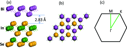
Our calculations are carried out based on the density functional theory with PAW pseudopotential paw and PBE exchange-correlation functional pbe using VASP package vasp . The bulk -In2Se3 in-plane lattice constant is from our calculation, which is very close to the experimental value sIn2Se3 . The substrate is simulated by one QL (11))In2Se3(1111) with the bulk in-plane lattice constant and additional vacuum of more than 20Å normal to the surface as shown in Fig. 1(a) of side view and Fig. 1(b) of top view. During the structural relaxation, all the atoms are allowed to relax until the forces are smaller than 0.01 eV/Å. 600 eV kinetic energy cutoff and 11111 Gamma centered k-mesh sampling are adopted for total energy convergence. After structural relaxation the vertical distance between top Bi bilayer and bottom substrate is 2.83 , and the inter-layer binding energy is 0.3 eV/surface-unit-cell. This indicates that the interfacial interaction is much stronger than vdW bond but significantly weaker than typical chemical bond.


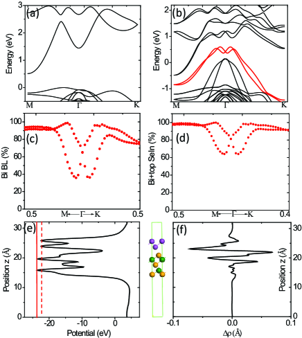
Fig. 2(a) and 2(b) show the band structures of bare one QL In2Se3 and Bi BL on In2Se3 along directions, respectively. In Fig. 2(a) we found that bare one QL In2Se3 has an indirect band gap of 0.5 eV with the conduction band minimum (CBM) at M point and that the band gap at other k-points away from M is larger than 1.0 eV. Most interestingly because the QL surface is from the cleavage through the vdW gap and does not break chemical bonds, there are no metallic surface states formed at the surface and the QL substrate still remains a semiconductor. We have verified that this behavior is not due to quantum confinement effect with our complementary calculation of the band structure of In2Se3(0001) substrate with significantly larger number of QLs, which shows that it is still a semiconductor except slight different band gap from that of one QL. In Fig. 2(b) the bands marked with red color shows Rashba-like splitting in the vicinity of point. Due to the spatial inversion symmetry, all bands in free-standing Bi BL are two-fold degenerated. If the interaction between Bi BL and the substrate is negligibly weak, the Bi BL will be chemically decoupled with the substrate and spatial inversion symmetry of Bi Bi is locally retained, and then Bi bands should not be split. Therefore, the inter-layer interaction must play a key role for the Bi band-splitting. It is well know that LDA/GGA underestimates the band gap of semiconductor. This may affect the band gap of the one-QL In2Se3 and also the energy position of the Rashba-like bands in the gap region. We thus used hybrid functional HSE to do the similar band structure calculations for bare one QL In2Se3 and Bi BL on In2Se3. We found that the energy gap becomes around 1.2 eV due to the valence band shift to the lower energy, but the relative position between the Rashba-like bands and the substrate conduction bands does not change. Therefore in the following all the results are from standard DFT calculations with PBE functional.
To get a physical insight of such interfacial interaction, we calculate the charge localization of the two Rashba split bands as a function of k-points along the as shown in Figs. 2(c) and (d) for charge distribution only from top Bi BL and top Bi BL + the top Se/In atomic layers, respectively. Around point, the states have comparable distributions in both Bi BL and substrate. This indicates that a sizable hybridization between Bi BL and substrate may occur for the states around . Away from , the charge almost all localizes in Bi BL, having little in the substrate. In Fig. 2(e) we plot the in-plane averaged electron potential along z direction. It is seen that the potential-well at Bi BL is asymmetric with the top potential higher at the interface between top Bi layer and vacuum than the bottom potential at the interface between bottom Bi layer and the substrate. This causes the top Bi layer is not equivalent to the bottom Bi layer and thus breaks the inversion symmetry that holds in free-standing Bi BL. The solid and dashed lines indicate the potential minima at the substrate QL and Bi BL respectively with substrate QL potential minimum lower than Bi BL. This indicates that the charge transfer between Bi-BL and the substrate will be from Bi-BL to the substrate. We then calculate the charge transfer () between Bi BL and the substrate along z direction in Fig. 2(f). Clearly, there is a substantial charge transfer at the interface. The Bi BL acts as an electron-donor and the In2Se3 substrate as an electron-acceptor, with the electrons transferring from the former to the latter. This is consistent with the result from the analysis of electron potential in Fig. 2(e). This charge transfer generates a large internal electric field at the interface region. The field direction points from the Bi to In2Se3 and field strength is estimated as high as 0.40 .
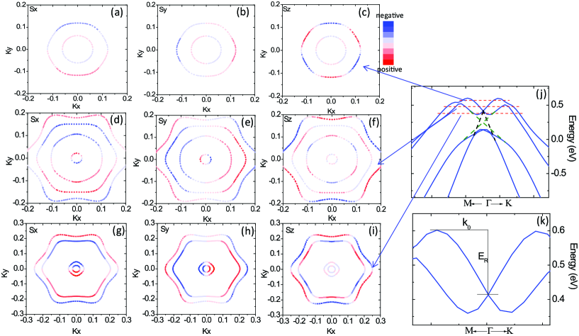
Such charge transfer induced band splitting is very similar to the external electric field induces Rashba band splitting in the surface state of topological insulators chenli ; SbTe . To clearly see this similarity, in Fig. 3(j) and (k) we zoom-in the Rashba-split bands from Fig. 2(b) around point. The resulting band structure is very different from that of single pair of free-electron Rashba-split bands and The gap openings around the avoid-crossing k-points are found. We use dashed red and blue lines to track back possible band structure for the situation without interaction between the bands. This gives two pairs of downward Rashba bands. Because of time reversal symmetry the the splitting bands are degenerated at point. The estimated Rashba energy (), offset k vector (k0) from and Rashba parameter () are 182 meV, 0.10 and 3.66 , respectively. Here, we would like to emphasize three characters of the Rashba-like splitting in our system. First the is comparable to the largest value that has ever been observed in Bi/Ag(111) Rashba8 . Second in Fig. 3(a)-(i) we show the spin textures for x, y and z component of spin polarization vector for the three isoenergy surfaces marked by red dashed lines as in in Fig. 3(j) (150 meV, 60 meV above and 40meV below the degenerate point at , respectively). The spin polarization is defined as polar : , where . Because there are four bands, it displays four isoenergy surfaces in Fig. (d)-(i). The isosurface is only isotropic having a circular shape for small k vector (less than 0.15 Å-1) around and begins to gain some anisotropy for larger k vector having hexagonal shape. For the Sz component it has very small value along the path of small k-vector but it acquires sizeable value with increasing k-vector. This is different from the isoenergy surfaces and spin textures of free-electron Rashba model with only potential gradient along z direction, where the isoenergy surface is isotroic and the Sz component is zero with only in-plane spin components. The anisotropic isoenergy surface and out-of-plane spin component can be attributed to the in-plane potential gradient imposed by the periodic crystal field. Similar behavior has been observed in many studies for Bi/Ag(111) surface alloying system Rashba8 and 3D topological Dirac surface state in Bi2Te3 SzTI . Third the Sz component oscillates periodically around the isosurface with a period of which reflects the in-plane threefold rotational symmetry and have the opposite phase above and below the spin degenerate point at , similar to the topological surface states of 3D Bi2Se3 osig .

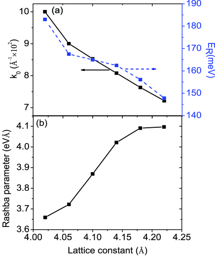
Lastly we notice that the In2Se3 substrate used is only one QL thick, hence it may be readily strained. Under substrate tensile strain, Bi BL can have less lattice mismatch with In2Se3 and in turn the Rashba parameter may be tuned with strain. Fig. 4(a) shows the strain dependence of k0 and ER with a tensile strain from to corresponding to inplane lattice constant from 4.02 to 4.22 . They both decrease with increasing lattice constant with k0 decreased by and ER decreased by . Fig. 4(b) shows that increases with increasing lattice constant and reaches 4.22 at inplane lattice constant of 4.22 . Such a trend of increase may be related to shorter vertical separation between Bi BL and the substrate which deceases from 2.83 at 4.02 lattice constant to 2.51 at 4.02 lattice constant, so that Bi BL feels larger electric field which induces larger .
The Indium Selenides family also has a few allotropes with different structures such as hexagonal and rhombohedral structures, and compositions such as InSe and In2Se3 vdW1 ; InSe1 ; InSe2 ; InSe3 . All of these allotropes have the similar layered structure with vdW type inter-layer bonding, which may give rise to the ”intermediate” interaction between the Bi BL and substrate. In addition, the band gaps of these allotropes range from 1.2 eV to 1.8 eV. Thus, we speculate that Bi BL may also grow on these substrates to create the Rashba spin splitting. The experimental work is expected to verify our proposal.
To summarize, we have investigated the electronic structures of Bi(111) BL grown on substrate of one-QL In2Se3, which has a large band gap of 1.2 eV and vdW like surface cleavage necessary for the stablization of Bi in (111) BL phase. Overlying Bi BL is predicted to have giant Rashba-like spin splitting in the substrate band gap. The interlayer interaction between Bi BL and In2Se3 is of ”intermediate” strength, which plays two important roles: (1) strong enough to induce sizable charge transfer and hence the Rashba-like strong spin splitting; (2) weak enough to avoid strong hybridization between Bi overlayer and substrate states and separate the substrate states from being in the energy range. These findings in this work may provide a good candidate substrate for Bi(111) film to realize spin splitting Rashba states with insignificant effect of spin degenerate states from the substrate.
This work was supported by NSF MRSEC (Grant No. DMR-1121252) and DOE-BES (Grant No. DE-FG02-04ER46148). We thank the CHPC at University of Utah and NERSC for providing the computing resources.
References
- (1) JunSaku Nitta, Tatsushi Akazaki, and Hideaki Takayanagi, Phys. Rev. Lett. 78, 1335 (1997).
- (2) S. LaShell, B. A. McDougall, and E. Jensen, Phys. Rev. Lett. 77, 3419 (1996).
- (3) D. Popovic, F. Reinert, S. Hufner, V. G. Grigoryan, M. Springborg, H. Cercellier, Y. Fagot-Revurat, B. Kierren and D. Malterre, Phys. Rev. B 72, 045419 (2005).
- (4) A. Varykhalov, D. Marchenko, M. R. Scholz, E. D. L. Rienks, T. K. Kim, G. Bihlmayer, J. Sanchez-Barriga, and O. Rader, Phys. Rev. Lett. 108, 066804 (2012).
- (5) Yu. M. Koroteev, G. Bihlmayer, J. E. Gayone, E. V. Chulkov, S. Blugel, P. M. Echenique, and Ph. Hofmann, Phys. Rev. Lett. 93, 046403 (2004).
- (6) K. Sugawara, T. Sato, S. Souma, T. Takahashi, M. Arai, and T. Sasaki, Phys. Rev. Lett. 96, 046411 (2006).
- (7) J. Hugo Dil, Fabian Meier, Jorge Lobo-Checa, Luc Patthey, Gustav Bihlmayer, and Jurg Osterwalder, Phys. Rev. Lett. 101, 266802 (2008).
- (8) Christian R. Ast, Jurgen Henk, Arthur Ernst, Luca Moreschini, Mihaela C. Falub, Daniela Pacile, Patrick Bruno, Klaus Kern, and Macro Grioni, Phys. Rev. Lett. 98, 186807 (2007).
- (9) I. Gierz, T. Suzuki, E. Frantzeskakis, S. Pons, S. Ostanin, A. Ernst, J. Henk, M. Grioni, K. Kern, and C. R. Ast, Phys. Rev. Lett. 103, 046803 (2009). Haijun Zhang, Chao-Xing Liu, Xiao-Liang Qi, Xi Dai, Zhong Fang, and Shou-Cheng Zhang, Nat. Phys. 5, 438 (2009). B. Andrei Bernevig, Taylor L. Hughes, and Shou-Cheng Zhang, Science 314, 1757 (2006).
- (10) S. Datta, and Das, Appl. Phys. Lett. 56, 665 (1990).
- (11) S. V. Eremeev, I. A. Nechaev, Yu. M. Koroteev, P. M. Echenique, and E. V. Chulkov, Phys. Rev. Lett. 108, 246802 (2012).
- (12) . M. Sakano, M. S. Bahramy, A. Katayama, T. Shimojima, H. Murakawa, Y. Kaneko, W. Malaeb, S. Shin, K. Ono, H. Kumigashira, R. Arita, N. Nagaosa, H. Y. Hwang, Y. Tokura, and K. Ishizaka, Phys. Rev. Lett. 110, 107204 (2013).
- (13) S. Murakami, Phys. Rev. Lett. 97, 236805 (2006).
- (14) Zheng Liu, Chao-Xing Liu, Yong-Shi Wu, Wen-Hui Duan, Feng Liu, and Jian Wu, Phys. Rev. Lett. 107, 136805 (2011).
- (15) T. Nagao, et al., Phys. Rev. Lett. 93, 105501 (2004).
- (16) S.Yaginuma, et al., Surf. Sci. 601, 3593 (2007).
- (17) J. T. Sadowski, et al., J. Appl. Phys. 99, 014904 (2006).
- (18) T. Nagao, et al., Surf. Sci. 590, L247 (2005).
- (19) S. A. Scott, et al., Surf. Sci. 587, 175 (2005).
- (20) A. Klein, O. Lang, R. Schlaf, C. Pettenkofer and W. Jaegermann, Phys. Rev. Lett. 80, 361 (1998).
- (21) Atsushi Koma, J. Cryst. Growth 201, 236 (1999).
- (22) Toru Hirahara, Gustav Bihlmayer, Yusuke Sakamoto, Manabu Yamada, Hidetoshi Miyazaki, Shin-ichi Kimura, Stefan Blugel and Shuji Hasegawa, Phys. Rev. Lett. 107, 166801 (2001).
- (23) Lin Miao, Z. F. Wang, Wenmei Ming, Meng-Yu Yao, Meixiao Wang, Fang Yang, Y. R. Song, Fengfeng Zhu, Alexei V. Fedorov, Z. Sun, C. L. Gao, Canhua Liu, Qi-Kun Xue, Chao-Xing Liu, Feng Liu, Dong Qian, and Jin-Feng Jia, PNAS 110, 2758 (2013).
- (24) G. Kresse and D. Joubert, Phys. Rev. B 59, 1758 (1999).
- (25) J. P. Perdew, K. Burke, and M. Ernzerhof, Phys. Rev. Lett. 77, 3865 (1996).
- (26) G. Kresse and J. Furthmler, Comput. Mat. Sci. 6, 15(1996).
- (27) Kozo Osamura, and Yataro Murakami, J. Phys. Soc. Japan 21, 1848 (1966).
- (28) J. Heyd, G. E. Scuseria, and M. Ernzerhof, J. Chem. Phys. 118, 8207 (2003); 124, 219906 (2006).
- (29) Minsung Kim, Choog H. Kim, Heung-Sik Kim and Jisoon Ihm, PNAS 109, 671 (2011).
- (30) Li Chen, Z. F. Wang, and Feng Liu, Phys. Rev. B 87, 235420 (2013).
- (31) O. Yazyev, et al., Phys. Rev. Lett. 105, 266806 (2010).
- (32) S, Souma, et al., Phys. Rev. Lett. 106, 216803 (2011).
- (33) Y. Zhao, et al., Nano Lett. 11, 2088 (2011)
- (34) P. Gomes da Costa, et al., Phys. Rev. B 48, 14135 (1993)
- (35) Jiping Ye, Sigeo Soeda, Yoshio Narkamura and Osamu Nittono, Jpn. J. Appl. Phys. 37, 4264 (1998);
- (36) Hailin Peng, Chong Xie, David T. Schoen and Yi Cui, Nano lett. 8, 1511 (2008)