Graphene on boron-nitride: Moiré pattern in the van der Waals energy
Abstract
The spatial dependence of the van der Waals (vdW) energy between graphene and hexagonal boron-nitride (h-BN) is investigated using atomistic simulations. The van der Waals energy between graphene and h-BN shows a hexagonal superlattice structure identical to the observed Moiré pattern in the local density of states (LDOS) which depends on the lattice mismatch and misorientation angle between graphene and h-BN. Our results provide atomistic features of the weak van der Waals interaction between graphene and BN which are in agreement with experiment and provide an analytical expression for the size of the spatial variation of the weak van der Waals interaction. We also found that the A-B-lattice symmetry of graphene is broken a long the armchair direction.
Two-dimensional (2D) atomic crystals, such as graphene, hexagonal boron nitride (h-BN), and molybdenum disulphide have gained recently a lot of interest both experimentally and theoretically 1 ; Dean . The possibility of producing heterostructures and devices made by stacking different 2D crystals on top of each other is another interesting research area. The in-plane strong covalent bonds provide in-plane stability for those 2D crystals whereas stacked layers are held together by the weak van der Waals-like forces 1 .
On the other hand graphene’s carrier mobility when deposited on a SiO2 substrate is limited due to scattering on substrate roughness, charged surface states and impurities Dean . Alternatives for SiO2 have been typically other oxides imposing similar surface effects and problems 3 . However, it was found that h-BN is an ideal substrate dielectric which is atomically flat and improved graphene’s mobility by more than two orders of magnitude. The B-N bond length is close to that of C-C with only a very small (1.6-2) lattice mismatch 4 . Different on-site energies for the B and N atoms lead to a large band gap in h-BN which differs from the zero gap in graphene 5 . These dielectric properties of h-BN are comparable with that of SiO2 making h-BN a promising alternative substrate for graphene with improved high-temperature and high-electric field performance. The latter is due to almost twice larger surface optical phonon frequency of h-BN than similar modes in SiO2 4 .
Moiré patterns are observed in aligned graphene on h-BN. It was found that graphene flakes can align with the underlying h-BN lattice within an error of less than 0.05o 4 ; 6 . The sizable Moiré superstructure pattern has a periodicity 4 much larger than the lattice constant of both graphene and h-BN, i.e. 140 Å. Ab-initio and semi-empirical van der Waals studies showed that the interaction between the small graphene flakes and the h-BN substrate is similar to that of a graphene-graphene stacked structure. The latter is deduced from the absence of net charge transfer between graphene and the h-BN layer 7 .
The mismatch between the honeycomb lattice structures of GE and h-BN leads to long wavelength Moiré patterns which requires large size unit cells that are unattainable with ab-initio calculations. Earlier density functional theory calculations assumed lattice matching between graphene and h-BN which induces strain and opens a gap in graphene’s spectrum of 4 meV SACH which was not observed experimentally pekhers . In previous works the Moiré pattern in GE/h-BN was connected to the van der Waals (vdW) interaction, but a clear theoretical microscopic analysis is still missing. We use molecular modeling and atomistic simulations with very large computational unit cells to study quantitative aspects of the connection between the vdW interaction and the Moiré pattern. Our results agree with recently reported experiments on the Moiré pattern in the LDOS of graphene on h-BN.
In order to include the vdW interaction between GE and h-BN we use a Lennard-Jones potential which models both the short range repulsive and long range attractive nature of the interaction between two particles. The LJ potential is a widely used potential in various simulations for two interacting particles, i.e. , where r is the distance between two atoms, is the depth of the potential well, and is the distance at which the potential becomes zero. To model the interaction between B, N and C atoms, we adjust the LJ parameters using the equations and where refer to B, N or C and where =3.369 Å , =3.453 Å, =3.365 Å and =2.635 meV, =4.16 meV, and =6.281 meV 8 ; 9 . The total vdW-energy of GE/h-BN has contributions both from B and N atoms, i.e. U=.
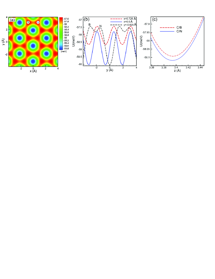
First, we calculate the vdW energy of a single C atom over a h-BN sheet at zero temperature which is depicted in Fig. 1(a) where the C atom is located at 3.4 Å above h-BN. The honeycomb lattice structure of the energy surface shows that a single C atom will be preferentially adsorbed onto the hollow sites. However since the depth of the wells are about 2 meV (which is negligible in comparison to the thermal energy at room temperature, i.e. 25 meV), the motion of a single C atom will be diffusive 10 . In Fig. 1(b) three cross sections of Fig. 1(a) along the zigzag (i.e. -axis where =0.0 and 0.725Å) and armchair (i.e. -axis, where =-0.625Å) directions are shown. It is seen that the potential profiles are different periodic functions. The variation of the total vdW energy of C/h-BN with height above the N (and B) site are shown in Fig. 1(c). The minimum energy, i.e. -58.12 meV (-58.09meV) is at 3.392 Å (3.395 Å ).
Next we study the vdW energy of a GE sheet over a h-BN substrate. The small mismatch between the two lattices implies that it is necessary to take a very large unit cell. One can simply estimate the superlattice size by solving the equation for two integer numbers and , where and are lattice vectors of h-BN and GE, respectively. We use two different sets of common bond lengths, i.e. =1.45 Å (1.44 Å) and =1.42 Å for the h-BN and GE sheets 4 ; 5 , respectively which results in a lattice mismatch of 0.021 (0.014). Furthermore, the two lattices may have different orientation which is determined by the misorientation angle . The difference between the two wave vectors of the graphene and h-BN lattices leads to the appearance of a hexagonal superlattice structure, i.e. Moiré pattern with length
| (1) |
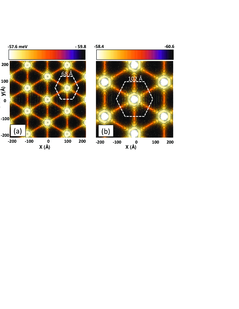
From the above values for and one can estimate =48/47(72/71) for which results in a superlattice with honeycomb structure with side 68 Å (102 Å). Thus the total number of atoms within such a unit cell, e.g. for becomes (and 20216 for ) which is beyond the ability of ab-initio methods.
Figure 2 shows density plots of the vdW energy surface per atom i.e. for the ith C atom we calculated where the summation is taken over all B and N atoms with (a) =1.45 Å and (b) =1.44 Å where in both cases . It is interesting that the honeycomb lattice structure in the vdW energy surface has lattice sides equal to 68 Å for (a) and 102 Å for (b) when the lattice mismatch is and , respectively. These results are in agreement with the hexagonal structure for the Moiré pattern reported in a recent experiment 4 , i.e. Å.
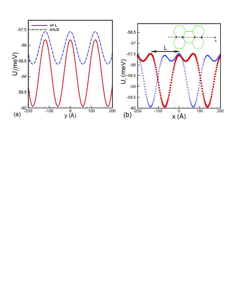
Moreover the depth of the energy wells are about that found for C/h-BN but the periodicity is very different. When we rotate the GE sheet over h-BN and recalculate the vdW energy we find a rotational symmetry. Therefore the global minimum energy of GE/h-BN occurs for with an integer number. Two cross sections of the energy surface of Fig. 2(a) in two perpendicular directions are shown in Fig. 3(a) (along zig-zag direction where Å) and Figs. 3(b) (armchair direction where 1.84 Å). It is seen that the vdW energy varies sinus-like along the zig-zag direction (with a wavelength of about 120 Å) while it shows a more complex behavior along the armchair direction. Notice that the energy along the armchair direction depends on the A-lattice and B-lattice cites of the graphene lattice, i.e. for a fix value , see inset of Fig. 2(b). Therefore, the vdW interaction breaks the A-B symmetry of the graphene sheet along the armchair direction while along the zig-zag direction we found .
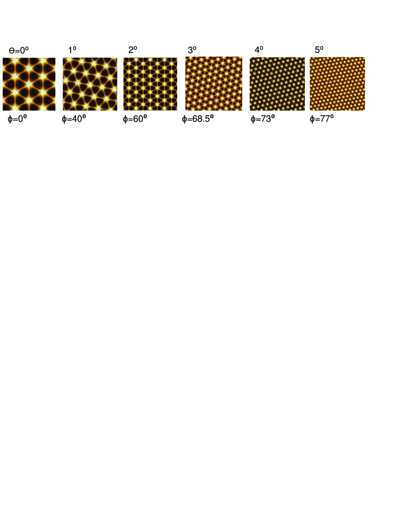
The effect of the misorientation () on the vdW superlattice structure is shown in Fig. 4 for Å. By changing from zero to , the vdW superlattice structure rotates over an angle
| (2) |
with respect to the h-BN sheet.
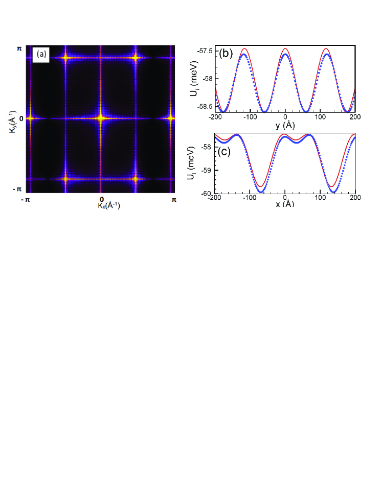
The Fourier transform (FT) of (Fig. 2(a)) is shown in Fig. 5. The seven large Fourier components in the FT of motivates us to approximate the Moiré pattern in the vdW energy by an analytical potential function. In analogy with the modulation function used in Refs. 4 ; Wallbank to describe the low energy spectrum of graphene’s Dirac electron, i.e. , where is the Fermi velocity, is a vector of Pauli matrices. We used six reciprocal lattice vectors, with where the modulation function can be written as , where is the rotation matrix about the -axis over an angle . The modulation function can be simplified and we found for the variation of the vdW energy
| (3) |
where is the offset energy and is the depth of the potential. The corresponding force on each carbon atom due to the interaction with the h-BN sheet can be written as
| (4) |
In Figs. 5(b,c) we compare the results of our analytical approximation (i.e. shown by solid lines) along the zig-zag () (b) and armchair () (c) directions with our simulation results (symbols). The numerical results are in close agreement with our atomistic simulation. Therefore this analytical expression can be useful to calculate different properties of graphene over h-BN sheet.
In order to check the accuracy of our atomistic simulations we calculated the total vdW energy stored between GE and h-BN as function of the inter-sheet distance. Our classical pair wise potential gives an equilibrium distance of 3.38 Å that is very close to previous first principal calculations for the adhesion energy SACH , i.e. 3.35 Å (the distance for the unit cell which gives the lowest energy (type IV in Ref. SACH )). The minimum energy of 60 meV is also equal to the reported energy obtained by using DFT calculations giovan ; APL2011 .
In summary, the vdW interaction between GE and h-BN was investigated for large size GE samples over h-BN. We found that the vdW energy surface exhibits a superlattice structure with size in the range 68-102 Å depending on the lattice mismatch which is in agreement with recently measured Moiré superlattice size of 80 Å. The used model for the vdW interaction enables us to perform atomistic simulations for large sample GE/h-BN and enabled us to present an analytical approximate expression for the spatial varying vdW energy. We found that the A-B sublattice symmetry in graphene is broken along the arm-chair direction. Our atomistic results for the total vdW energy between graphene and a BN sheet are in agreement with recent DFT calculations. The present study provides more physical insights on the weak interaction between graphene and a hexagonal boron nitride sheet.
Acknowledgment: This work was supported by the Flemish Science Foundation (FWO-Vl) and the Methusalem Foundation of the Flemish Government. M.N.-A was supported by the EU-Marie Curie IIF postdoc Fellowship/299855.
References
- (1) A. K. Geim and I. V. Grigorieva, Nature 499, 419 (2013).
- (2) C. R Dean, A. F. Young, I. Meric, C. Lee, L. Wang, S. Sorgenfrei, K. Watanabe, T. Taniguchi, P. Kim, K. L. Shepard, and J. Hone, Nature Nanotechnol. 5, 722 (2010).
- (3) J-H. Chen, C. Jang, S. Xiao, M. Ishigami, and M. S. Fuhrer, Nature Nanotechnol. 3, 206 (2008).
- (4) Shujie Tang, Haomin Wang, Yu Zhang, Ang Li, Hong Xie, Xiaoyu Liu, Lianqing Liu, Tianxin Li, Fuqiang Huang, Xiaoming Xie, and Mianheng Jiang, Scientific Reports 3, 2666 (2013).
- (5) J. Beheshtian, A. Sadeghi, M. Neek-Amal, K. H. Michel, and F. M. Peeters, Phys. Rev. B 86, 195433 (2012).
- (6) A. H. Castro Neto, F. Guinea, N. M. R. Peres, K. S. Novoselov, and A. K. Geim, Rev. Mod. Phys. 81, 109 162 (2009).
- (7) M. Yankowitz, J. Xue, D. Cormode, J. D. Sanchez-Yamagishi, K. Watanabe, T. Taniguchi, P. Jarillo-Herrero, P. Jacquod, and B. J. LeRoy, Nature Phys. 8, 382 (2012).
- (8) V. Caciuc, N. Atodiresei, M. Callsen, P. Lazic, and S. Blüge, J. Phys.: Condens. Matter 24, 424214 (2012).
- (9) B. Sachs, T. O. Wehling, M. I. Katsnelson, and A. I. Lichetensteinn, Phys. Rev. B 84, 195414 (2011); M. Zarenia, O. Leenaerts, B. Partoens, and F. M. Peeters, Phys. Rev. B 86, 085451 (2012).
- (10) J. Xue, J. Sanchez-Yamagishi, D. Bulmash, P. Jacquod, A. Deshpande, K. Watanabe, T. Taniguchi, P. Jarillo-Herrero, and Brian J. LeRoy, Nat. Mat. 10, 282 (2011); L. A. Ponomarenko, R. V. Gorbachev, G. L. Yu, D. C. Elias, R. Jalil, A. A. Patel, A. Mishchenko, A. S. Mayorov, C. R.Woods, J. R.Wallbank, M. Mucha-Kruczynski, B. A. Piot, M. Potemski, I. V. Grigorieva, K. S. Novoselov, F. Guinea, V. I. Fall’ko, and A. K. Geim, Nature (London)10, 282 (2011);
- (11) D. Baowan and J. M. Hill, Micro, Nano Letters, 2, 46 (2007).
- (12) J. Lee, J. Korean Phys. Soc. 49, 172 (2006).
- (13) M. Neek-Amal and A. Lajevardipour, Computational Materials Science 49, 839 (2010).
- (14) J. R. Wallbank, A. A. Patel, M. Mucha-Kruczynski, A. K. Geim, and V. I. Fal‘ko, Phy. Rev. B 87, 245 (2013).
- (15) G. Giovannetti, P. A. Khomyakov, G. Brocks, P. J. Kelly, and J. van den Brink, Phys. Rev. B 76, 073103 (2007).
- (16) Y. Fan, M. Zhao, Z. Wang, X. Zhang, and H. Zhang, Applied Phys. Lett. 98, 083103 (2011)