All-Electron GW Quasiparticle Band Structures of Group 14 Nitride Compounds
Abstract
We have investigated the group 14 nitrides (M3N4) in the spinel phase (-M3N4 with M= C, Si, Ge and Sn) and phase (-M3N4 with M= Si, Ge and Sn) using density functional theory with the local density approximation and the GW approximation. The Kohn-Sham energies of these systems have been first calculated within the framework of full-potential linearized augmented plane waves and then corrected using single-shot G0W0 calculations, which we have implemented in the modified version of the Elk full-potential LAPW code. Direct band gaps at the point have been found for spinel-type nitrides -M3N4 with M= Si, Ge and Sn. The corresponding GW-corrected band gaps agree with experiment. We have also found that the GW calculations with and without the plasmon-pole approximation give very similar results, even when the system contains semi-core electrons. These spinel-type nitrides are novel materials for potential optoelectronic applications because of their direct and tunable band gaps.
I Introduction
Group 14 nitride compounds, M3N4 (M=C, Si, Ge and Sn), are an important class of semiconductors. Among them is silicon nitride (Si3N4), which has been extensively studied by theoretical and experimental groupsChing et al. (2000); Kruger et al. (1997); Bradley et al. (1966); Pham et al. (2011); Liu and Cohen (1990); Borgen and Seip (1961); Ruddlesden and Popper (1958). It is known that Si3N4 can exist in two energetically favorable phases, - and -Si3N4, which have hexagonal crystal structures with different stacking patterns of the layered atoms perpendicular to the axis. Since the first discovery of Si3N4 in a third phase, the cubic spinel phaseZerr et al. (1999) (-Si3N4) reported in 1999, this class has stimulated great research efforts in the past few yearsYang et al. (2007); Dong et al. (2000); Ching et al. (2002); Ching and Rulis (2006); Mo et al. (1999); Kuwabara et al. (2008); Boyko et al. (2013); Pradhan et al. (2010); Huang and Feng (2004). -Ge3N4 and -Sn3N4 have also been synthesized successfully in subsequent experimentsScotti et al. (1999); Serghiou et al. (1999a, b), however -C3N4 has not yet been found experimentally. Whereas -Si3N4 and -Ge3N4 are synthesized in a high-temperature and high-pressure environment, the synthesis of -Sn3N4 can be achieved at ambient conditions. These novel spinel compounds exbihit remarkable mechanical properties and high thermal stability, and they form a new class of superhard materials. Also, with interesting electronic properties such as direct and tunable band gaps, these materials are good candidates for optoelectronic applications, e.g. light-emitting diodes.
Previous ab initio electronic structure calculations were carried out for these nitride compounds in different phasesChing et al. (2000); Yang et al. (2007); Dong et al. (2000); Ching et al. (2002, 2001); Hu et al. (2006). The methods used were mainly based on density functional theory (DFT)Kohn and Sham (1965), either within the orthogonalized linear combinations of atomic orbitals (OLCAO) methodChing and Lin (1975) or the plane-wave pseudopotential method. The studies concerning electronic band gaps are important for a variety of potential applications. However, it is well known that DFT is a ground-state theory and it severely underestimates the band gap, which relates to the functional derivative discontinuity of the exchange-correlation potential. The DFT Kohn-Sham (KS) energies may also not match the quasiparticle energies because of a lack of many-body interactions. The standard calculation including many-body corrections uses the GW approximation proposed by HedinHedin (1965) within the framework of many-body perturbation theory. Recently, Kresse et al.Kresse et al. (2012) have studied the GW-corrected electronic properties of - and -Si3N4. Gao et al.Gao et al. (2013) have applied the GW approach to study the band gaps for -, - and -Ge3N4. Xu et al.Xu and Gao (2012) have studied the GW quasiparticle energies of the C3N4 polymorphs. All these calculations have been performed using the plane-wave based pseudopotential or projected augmented wave (PAW)Blöchl (1994) method. In current practice, neither pseudopotential nor PAW methods includes GW for core level corrections and there is evidence that the GW results calculated using the pseudo wave functions might lead to errors compared with those using the all-electron wave functionsGómez-Abal et al. (2008); Li et al. (2012).
Another common approximation uses the fact that the inverse dielectric matrix is usually peaked around the plasma frequency but very flat elsewhere. This plasmon-pole approximation (PPA) is often introduced to simplify the frequency dependence of that matrix and to speed up the GW calculations. The PPA has been found to yield band gaps close to experimental results. However, it is also known that the results from different PPA modelsHybertsen and Louie (1986); Godby and Needs (1989); von der Linden and Horsch (1988); Engel and Farid (1993) may vary substantially when compared with those from the numerical integration (NI) method, due to the different parameter-fitting conditions. Recent studies show that the PPA model proposed by Godby and Needs (GN)Godby and Needs (1989) agrees consistently with the NI methodShaltaf et al. (2008); Stankovski et al. (2011); Larson et al. (2013), however it has been discussed that the PPA can become questionable when it is applied to systems with localized electronsAryasetiawan and Gunnarsson (1998), e.g. semi-core electrons. A careful study on this issue is therefore needed.
In this work, we have investigated the electronic structures of the -M3N4 (M=C, Si, Ge and Sn). The DFT KS eigenvalues and eigenfunctions have been computed within the framework of the full-potential linearized augmented plane wave (LAPW) method, which does not require pseudopotentials. We have then used the KS energies as input for the single-shot G0W0 to compute the quasiparticle energies. We have also studied the -M3N4 (M= Si, Ge and Sn), in which the phase is found to be more energetically stable for Si3N4 and Ge3N4. In the GW calculations, both the GN-PPA model and the NI method have been used and results have been compared. The rest of the article is organized as follows: we give a brief overview of the GW formalism including details of our implementation in Section II, describe our model systems and the computational details in Section III, present our results in Section IV, and end with conclusions in Section V.
II Methodology
II.1 The GW method
Within the single-particle picture, the quasiparticle equation reads
| (1) | |||
where , and are the kinetic energy operator, the external potential from the nuclei and the Hartree potential, respectively. is the self-energy operator that accounts for all the many-body electron-electron interactions beyond the Hartree term. In general, the self-energy is energy-dependent, non-local and non-Hermitian. This leads to complex quasiparticle energies of which the imaginary part relates to the quasiparticle lifetime. In Eq.(1), since the self-energy depends on , this equation has to be solved self-consistently, which is computationally very expensive.
The practical method for calculating the self-energy employs the GW approximationHedin (1965), in which the self-energy is expanded and only the first-order term is retained. When expressed in real space, the self-energy within this approximation reads as
| (2) |
where is the single-particle Green function, is a positive infinitesimal and is the dynamically screened Coulomb potential, with and being the dielectric function and the bare Coulomb potential. The dielectric function can be constructed using the density-density response function in the random phase approximation (RPA), which is detailed in the next sub-section.
In conventional GW calculations, the quasiparticle eigenfunctions are approximated as the DFT Kohn-Sham (KS) eigenfunctions. This is based on previous observations that the quasiparticle eigenfunctions change little compared with the KS eigenfunctions. The self-energy matrix in the KS basis becomes diagonal, i.e. only the diagonal elements of the self-energy matrix need to be evaluated. For single-shot G0W0, in which one non-self consistent GW loop is performed, the KS eigenvalues and eigenfunctions are used to construct the non-interacting Green function and the screened potential , and hence the self-energy. The quasiparticle energies can then be calculated using first-order perturbation theory:
| (3) | |||
| (4) |
Here, , is known as the renormalization factor for the KS state with band index and wave vector . is the KS exchange-correlation potential.
II.2 Evaluation of the self-energy
We have implemented the G0W0 approach in the modified version of the Elk full-potential LAPW codeKozhevnikov et al. (2010). To calculate the self-energy matrix in the KS basis, we have split it into two terms: where is the exchange self-energy matrix whose elements are known as the Fock terms in the Hartree-Fock approximation. is the correlation self-energy matrix. within the KS basis, can be written as
where the KS eigenfunctions {} are expressed in spinor form, i.e. . In this work, we have directly calculated the exchange self-energy matrix elements in real space. We have found that within the framework of the full-potential LAPW method, such elements cannot be evaluated efficiently in reciprocal space due to the extremely slow convergence with respect to the reciprocal lattice vectors. It is important to point out that when computing exchange self-energy elements, contributions from both the core and valence electrons have to be included to account for the important core-valence exchange processKu and Eguiluz (2002).
Unlike , the correlation self-energy within the KS basis can be evaluated efficiently in reciprocal space, and it reads
| (6) | |||||
where . This matrix contains all the information regarding the KS eigenfunctions. is the Fourier transform of the bare Coulomb potential. is the non-interacting Green function written in and space with being the occupation number of state . The dummy variable runs over all the valence and conduction bands, and the integration over is within the first Brillouin Zone (BZ) of reciprocal space. is the frequency-dependent term of the RPA inverse dielectric matrix. Its element reads , where is the RPA dielectric matrix element, which reads
| (7) |
where is the non-interacting density-density response function constructed using the KS eigenvalues and eigenfunctions,
| (8) | |||||
Note that a convolution along the axis is needed in Eq.(6), which requires an inversion of the dielectric matrix at all points. In this work, a direct evaluation of this convolution has been referred to as the NI method. In the current implementation of this method, is first computed on a set of points and linear interpolation is employed between any two neighbouring points for computing the convolution.
Apart from the NI method, the PPA has also been implemented and tested. Within the PPA, the frequency dependence of is simplified and is approximated by a single-pole function of that reads
| (9) | |||||
where and are the two matrices that need to be determined. We have adopted the fitting approach proposed by Godby and Needs (GN)Godby and Needs (1989). To do this, is evaluated both at and where is set as 1 Ha throughout this work.
Within the PPA, the correlation self-energy becomes
| (10) | |||||
| (11) | |||||
It is worth pointing out that when computing the correlation self-energy elements using either the NI method or the PPA, deep core electrons are neglected due to their small contribution. In contrast, the relatively shallow core electrons are included and treated on the same footing as valence electrons.Usuda et al. (2002)
III Model systems and computational details
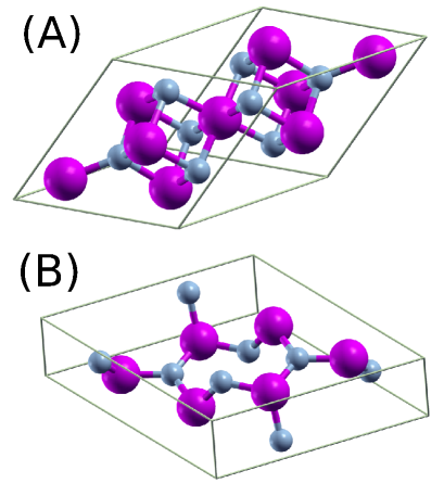
The group 14 nitride compounds in the cubic spinel phase, -M3N4, and in the phase, -M3N4 have been studied in this work. Here, M= C, Si, Ge and Sn for -M3N4; M= Si, Ge and Sn for -M3N4. The space groups for -M3N4 and -M3N4 are -3 (227) and (176), respectively. The -M3N4 has a face-centered cubic (FCC) structure while the -M3N4 has a hexagonal structure. In both phases, there are six M and eight N atoms in the primitive cell (see Fig. 1).
| System | ) ( eV ) | |||||
|---|---|---|---|---|---|---|
| LDA | G0W(PPA) | G0W(NI) | Expt. | |||
| -C3N4 | 6.675 | 1.17 | 1.96 | 1.96 | ||
| -Si3N4 | 7.697 | (7.80) | 3.35 | 4.87 | 4.89 | 4.6-5.0 |
| -Ge3N4 | 8.211 | (8.2063) | 2.07 | 3.26 | 3.27 | 3.3-3.7, 3.50 |
| -Sn3N4 | 9.001 | (9.037) | 0.58 | 1.53 | 1.42 | 1.4-1.8 |
All the calculations have been performed using the modified version of the Elk full-potential LAPW code, in which we have implemented the G0W0 approach as described in Section II B. For the DFT calculations, the exchange-correlation functionals have been treated within the local density approximation (LDA). When expanding the intersitial potential, the maximum length of the reciprocal lattice vector has been selected as 12 a.u. The first BZ has been sampled by a mesh for the spinel-type structures and a mesh for the -phase structures. All the above parameters have carefully been tested for total energy convergence. The atomic structures for all the systems have been optimized until the force components on each atom are less than 0.05 eV/å. In the calculations concerning the Ge and Sn, the Ge and Sn electrons have been treated as valence electrons.
For the GW calculations, 400 conduction bands have been used for computing the dielectric matrix and the Green function. Note that the GW band gap in all the systems only varies less than 0.04 eV when the number of conduction bands is reduced by a factor of two. This fast convergence regarding the band gap is likely due to the error cancellation between the quasiparticle energy corrections of the valence and conduction bands. We have used 61 frequency points for the NI method.
IV Results
IV.1 -M3N4
First, we have investigated the -M3N4 compounds. The structural optimization has been carried out for each system and the resulting lattice parameters are given in Table I. For -Si3N4, -Ge3N4 and -Sn3N4, they are in very good agreement with the experimental lattice parameters. The percentage difference is about 1 or less.
The DFT-LDA electronic band gaps have been computed and the direct gap values at , are illustrated in Table I. For -Si3N4, -Ge3N4 and -Sn3N4, we have found that the minimal band gap is always direct at . For the hypothetical -C3N4, however, the band gap is found indirect and is 0.17 eV smaller than . In this case, the conduction band minimum (CBM) is located at whereas the valence band maximum (VBM) is near the point (0.75, 0.25, 0.00), expressed in fractional coordinates of the primitive reciprocal lattice vectors. This is contrary to other theoretical findingsChing et al. (2001) that the minimal band gap in this system is found direct at . Moreover, our DFT-LDA for -C3N4, -Si3N4 and -Ge3N4 are very similar to those obtained by the plane-wave based pseudopotential methods, with the difference always less than 0.2 eV. This indicates that pseudopotential methods yield only small errors in the calculations for these compounds. For -Sn3N4, our band gap is about 0.7 eV less than that from other theoretical calculationsChing et al. (2001).
The DFT-LDA band gaps are consistently underestimated, and are at least 0.8 eV smaller compared with the available experimental counterparts. To improve accuracy, we have performed the single-shot G0W0 calculations using the PPA or the NI method for the band gaps (see Table I). For -C3N4, -Si3N4 and -Ge3N4, the GW band gaps using the PPA are remarkably close to those using the NI method. For the -Sn3N4, the band gap difference is 0.11 eV between the two methods. Overall, our results agree with the previous studies which claim that the GN-PPA results can consistently match the NI counterpartsStankovski et al. (2011); Larson et al. (2013). Using either method, the computed band gaps are in good agreement with experiments (see Table I).
| System | ( eV ) | |||||||
|---|---|---|---|---|---|---|---|---|
| LDA | G0W(PPA) | G0W(NI) | Expt. | |||||
| -Si3N4 | 7.576 | (7.607) | 2.892 | (2.911) | 4.19 | 6.06 | 6.06 | |
| -Ge3N4 | 8.063 | (8.038) | 3.084 | (3.074) | 2.03 | 3.60 | 3.59 | 4.4-4.8 |
| -Sn3N4 | 8.814 | 3.418 | 0.13 | 1.04 | 0.98 |
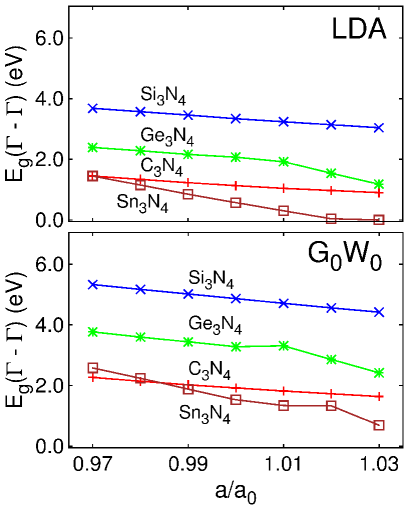
To understand the impact of the lattice parameter on the electronic band gap, we have performed calculations at both the DFT-LDA and the G0W0 levels. In these calculations, varies between 0.97 to 1.03 times the optimized lattice parameter, given in Table I. The results are illustrated in Fig. 2. At each given , the DFT-LDA structural optimization has been first employed for the lowest total energy. The same lattice parameter has then been adopted for the subsequent band gap calculations. Our results suggest that the band gap at is very sensitive to the lattice parameter. For -C3N4 and -Si3N4, the DFT-LDA results show that linearly decreases along with the increase of . For -C3N4, the trend for the indirect band gap is very similar to the one demonstrated and is not shown here. Within the range of , varies between 0.9 and 1.45 eV for -C3N4 and between 3.04 and 3.68 eV for -Si3N4. Upon the GW corrections, the curves for these two systems are shifted upward compared with the DFT-LDA results, which suggests that the band gap corrections due to the GW method stays almost the same as changes. For -Ge3N4, the DFT-LDA band gap also decreases linearly when increases. Within the range of , the DFT-LDA band gap varies between 1.18 and 2.39 eV. Note that the slope changes when becomes 1.01. Further investigation suggests that this variation stems from the symmetry change at the CBM: the CBM is triply degenerate when is smaller than 1.01, and becomes singly degenerate otherwise. Upon the GW correction, the curve has a similar trend as its DFT-LDA counterpart, and a kink appears at . The GW band gap correction varies little at different values. For -Sn3N4, the DFT-LDA band gap decreases linearly as increases until equals 1.02, at which point the band gap is reduced to 0.04 eV. At , the band gap becomes zero. The band gap variation in this range is 1.45 eV, which is 250 % more than the band gap at . With the GW correction included, the band gap monotonically decreases when increases. Note that the GW correction results in a non-zero band gap when , despite the zero gap predicted by the DFT-LDA calculations. Also, the band gap correction at is smaller compared with those at other values. This is due to the sign change (from negative to positive) of the correlation self-energy at the CBM.
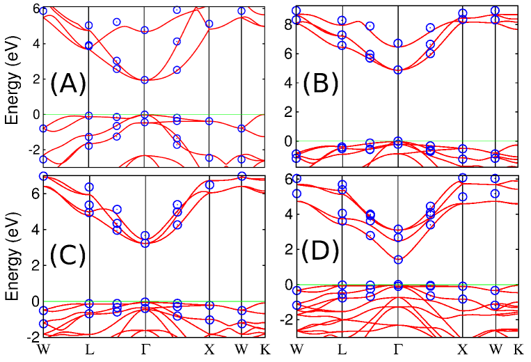
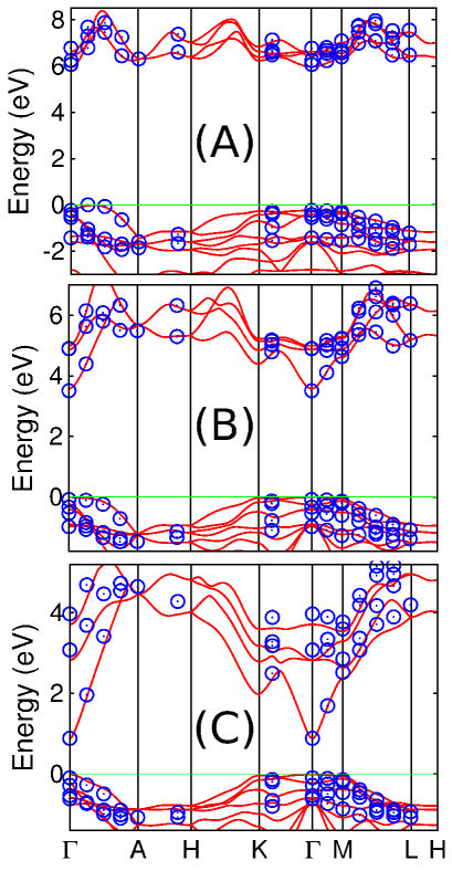
The DFT-LDA band structures for all the compounds at are demonstrated in Fig. 3, in which the conduction bands have been shifted upward using the corresponding GW-NI band gap values. With the use of the NI method, the GW quasiparticle energies for the four valence bands and four conduction bands near the band gap have also been shown in the figure (blue circles). We have found that after shifting the conduction bands using the GW-corrected band gap, the quasiparticle energies in the valence band are very close to their DFT counterparts, whereas in the conduction band the difference remains small only near the point. Since the VBM and CBM are both located at for the -Si3N4, -Ge3N4 and -Sn3N4, this indicates that the difference of the optical properties predicted by the DFT and by the GW method is mainly due to the band gap corrections. Our results also imply that the band gap property (direct or indirect) is conserved after the GW corrections have been applied.
IV.2 -M3N4
Next, we have studied the -M3N4 compounds with M=Si, Ge and Sn. Based on the available experimental data, -Sn3N4 remains hypothetical whereas the other two have been synthesized successfully. As a first step, their atomic structures have been optimized and the resulting lattice parameters and are given in Table II. For -Si3N4 and -Ge3N4, these parameters are in very good agreement with experiment (see Table II). The percentage difference is always less than 1 %.
The DFT-LDA band gaps are shown in Table II. For -Si3N4, the band gap at is 4.39 eV. This system is known as an indirect band-gap semiconductor. Based on our calculations, the minimal band gap is estimated as 4.19 eV, in which the CBM and VBM are located at and the -point (0, 0, 0.125) in fractional coordinates. For both the -Ge3N4 and the hypothetical -Sn3N4, the minimal band gap is at . Based on our calculations, the DFT-LDA band gap for the -Sn3N4 has been obtained as 0.13 eV. Upon the GW corrections using either the PPA or NI method, the band gaps are much larger than those DFT-LDA counterparts. For -Ge3N4, the DFT-LDA band gap is 2.03 eV, which is much smaller than Gao et al.’s calculated value of 2.92 eVGao et al. (2013). This may be due to the different lattice parameters and used in the calculations: we have found that our and are both about 2% bigger than those computed using the pseudopotential method. If using 2% smaller all-electron lattice parameters for the DFT-LDA calculation, the band gap calculated by our method is 2.68 eV that matches well with the pseudopotential calculations. This suggests a strong dependence of the band gap on and (see Fig. 4) as seen for the other nitride compounds. Note that the corresponding GW band gap is 3.60 eV, which is smaller than 4.293 eV given in Gao et al.’s resultsGao et al. (2013), and is also 0.8 eV smaller than the experimental value. Based on the fact that our all-electron lattice parameters are in very good agreement with experiments, the band gap difference between our results and the experiments may result from the exclusion of self-consistency in the G0W0 method, and the band gap corrections may depend on the starting point, e.g. the LDA KS eigenvalues and eigenfunctions. A self-consistent GW approach can eliminate this dependency and may reduce the gap between the calculated and experimental results. More studies on this issue may be addressed in the future.
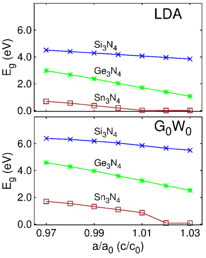
Next, we have studied the dependence of band gap on the lattice parameters and for these compounds. In our calculations, () varies between 0.97 and 1.03 with respect to (), the optimized lattice parameter given in Table II. The ratio has been kept unchanged in the calculations. Again, the structural optimization has been carried out at each selected pair of and . Then the band gap at both the DFT-LDA and G0W0 levels has been obtained. The results are illustrated in Fig. 4. For -Si3N4 and -Ge3N4, the DFT-LDA band gap linearly decreases as () increases. The corresponding GW band gaps follow the same trend, with an overall shift upward compared with the DFT-LDA results. This again suggests that the GW correction to the DFT-LDA band gap is weakly dependent on the varying () within this range. For -Sn3N4, the DFT-LDA band gap presents a decreasing trend when the lattice parameters increase before , and the gap value approaches zero when greater than 1.01. Our calculations indicate that the location of the VBM is changed when , which leads to an indirect band gap for this system. The corresponding GW band gap at and 1.03 is less than 0.1 eV.
The DFT-LDA band structures for the compounds at () have been illustrated in Fig. 5. Similarly, the conduction bands have been shifted upward using the GW-NI gap value. The GW quasiparticle energies for the four valence and four conduction bands are shown in the figure as well. In each case, the GW corrections are very small in the valence band, whereas the corrections in the conduction band are small near the CBM at . Our GW calculations also suggest direct band gaps at for the -Ge3N4 and -Sn3N4.
V Conclusions
To summarize, we have studied the electronic properties of the group 14 nitride compounds in the spinel phase -M3N4 (M=C, Si, Ge and Sn) and the phase -M3N4 (M=Si, Ge and Sn) within the framework of the full-potential LAPW method. The lattice parameters obtained by the structural optimization are in good agreement with experiments. For the spinel-type structures -M3N4, direct band gaps at have been found for M=Si, Ge and Sn, whereas the band gap is indirect for the hypothetical -C3N4. Using single-shot G0W0 corrections to account for many-body interactions, the band gaps agree very well with the experimental data for the spinel structures. Moreover, our calculations at the DFT-LDA and G0W0 levels have shown a strong dependence of the band gap on the lattice parameters in both phases. In particular, the band gap always decreases as the lattice parameters increase. We have also compared our GW results based on the PPA to those obtained by the NI method. We have found that the GW-PPA band gaps for all the structures studied are consistently close to the GW-NI results, with a difference less than 0.11 eV.
Our GW calculations include the minimal approximations except for those in the G0W0 approach. In particular, the pseudopotential method, which has been widely used for the first-principles studies, is not required here. Our theoretical results for the predicted -C3N4 and -Sn3N4 can provide guidance for future experiments. The spinel-type nitrides -M3N4 (M=Si, Ge and Sn) in our study are novel high-pressure compounds that are very promising for optoelectronic applications.
VI Acknowledgements
This work is supported by NSF/DMR-0804407 and DOE/BES-DE-FG02-02ER45995. We acknowledge Dr. Yun-Peng Wang for helpful discussions. The calculations have been performed at NERSC and UF-HPC Center.
References
- Ching et al. (2000) W. Y. Ching, L. Ouyang, and J. D. Gale, Phys. Rev. B 61, 8696 (2000).
- Kruger et al. (1997) M. B. Kruger, J. H. Nguyen, Y. M. Li, W. A. Caldwell, M. H. Manghnani, and R. Jeanloz, Phys. Rev. B 55, 3456 (1997).
- Bradley et al. (1966) R. Bradley, D. Munro, and M. Whitfield, J. Inorg. Nucl. Chem. 28, 1803 (1966).
- Pham et al. (2011) T. A. Pham, T. Li, S. Shankar, F. Gygi, and G. Galli, Phys. Rev. B 84, 045308 (2011).
- Liu and Cohen (1990) A. Y. Liu and M. L. Cohen, Phys. Rev. B 41, 10727 (1990).
- Borgen and Seip (1961) O. Borgen and H. M. Seip, Acta Chem. Scand. 15, 1789 (1961).
- Ruddlesden and Popper (1958) S. N. Ruddlesden and P. Popper, Acta Cryst. 11, 465 (1958).
- Zerr et al. (1999) A. Zerr, G. Miehe, G. Serghiou, M. Schwarz, E. Kroke, R. Riedel, H. Fuesz, P. Kroll, and R. Boehler, Nature 400, 340 (1999).
- Yang et al. (2007) M. Yang, S. J. Wang, Y. P. Feng, G. W. Peng, and Y. Y. Sun, J. Appl. Phys. 102 (2007).
- Dong et al. (2000) J. Dong, O. F. Sankey, S. K. Deb, G. Wolf, and P. F. McMillan, Phys. Rev. B 61, 11979 (2000).
- Ching et al. (2002) W.-Y. Ching, S.-D. Mo, L. Ouyang, P. Rulis, I. Tanaka, and M. Yoshiya, J. Am. Chem. Soc. 85, 75 (2002).
- Ching and Rulis (2006) W. Y. Ching and P. Rulis, Phys. Rev. B 73, 045202 (2006).
- Mo et al. (1999) S.-D. Mo, L. Ouyang, W. Y. Ching, I. Tanaka, Y. Koyama, and R. Riedel, Phys. Rev. Lett. 83, 5046 (1999).
- Kuwabara et al. (2008) A. Kuwabara, K. Matsunaga, and I. Tanaka, Phys. Rev. B 78, 064104 (2008).
- Boyko et al. (2013) T. D. Boyko, A. Hunt, A. Zerr, and A. Moewes, Phys. Rev. Lett. 111, 097402 (2013).
- Pradhan et al. (2010) G. K. Pradhan, A. Kumar, S. K. Deb, U. V. Waghmare, and C. Narayana, Phys. Rev. B 82, 144112 (2010).
- Huang and Feng (2004) M. Huang and Y. P. Feng, J. Appl. Phys. 96 (2004).
- Scotti et al. (1999) N. Scotti, W. Kockelmann, J. Senker, S. Traßel, and H. Jacobs, Z. Anorg. Allg. Chem. 625, 1435 (1999).
- Serghiou et al. (1999a) G. Serghiou, G. Miehe, O. Tschauner, A. Zerr, and R. Boehler, J. Chem. Phys. 111 (1999a).
- Serghiou et al. (1999b) G. Serghiou, G. Miehe, O. Tschauner, A. Zerr, and R. Boehler, J. Chem. Phys. 111 (1999b).
- Ching et al. (2001) W. Y. Ching, S.-D. Mo, I. Tanaka, and M. Yoshiya, Phys. Rev. B 63, 064102 (2001).
- Hu et al. (2006) J. Hu, W. Cheng, S. Huang, D. Wu, and Z. Xie, Appl. Phys. Lett. 89, 261117 (2006).
- Kohn and Sham (1965) W. Kohn and L. J. Sham, Phys. Rev. 140, A1133 (1965).
- Ching and Lin (1975) W. Y. Ching and C. C. Lin, Phys. Rev. B 12, 5536 (1975).
- Hedin (1965) L. Hedin, Phys. Rev. 139, A796 (1965).
- Kresse et al. (2012) G. Kresse, M. Marsman, L. E. Hintzsche, and E. Flage-Larsen, Phys. Rev. B 85, 045205 (2012).
- Gao et al. (2013) S.-P. Gao, G. Cai, and Y. Xu, Comput. Mater. Sci. 67, 292 (2013).
- Xu and Gao (2012) Y. Xu and S.-P. Gao, Int. J. Hydrogen Energ. 37, 11072 (2012).
- Blöchl (1994) P. E. Blöchl, Phys. Rev. B 50, 17953 (1994).
- Gómez-Abal et al. (2008) R. Gómez-Abal, X. Li, M. Scheffler, and C. Ambrosch-Draxl, Phys. Rev. Lett. 101, 106404 (2008).
- Li et al. (2012) X.-Z. Li, R. Gómez-Abal, H. Jiang, C. Ambrosch-Draxl, and M. Scheffler, New J. Phys. 14, 023006 (2012).
- Hybertsen and Louie (1986) M. S. Hybertsen and S. G. Louie, Phys. Rev. B 34, 5390 (1986).
- Godby and Needs (1989) R. W. Godby and R. J. Needs, Phys. Rev. Lett. 62, 1169 (1989).
- von der Linden and Horsch (1988) W. von der Linden and P. Horsch, Phys. Rev. B 37, 8351 (1988).
- Engel and Farid (1993) G. E. Engel and B. Farid, Phys. Rev. B 47, 15931 (1993).
- Shaltaf et al. (2008) R. Shaltaf, G.-M. Rignanese, X. Gonze, F. Giustino, and A. Pasquarello, Phys. Rev. Lett. 100, 186401 (2008).
- Stankovski et al. (2011) M. Stankovski, G. Antonius, D. Waroquiers, A. Miglio, H. Dixit, K. Sankaran, M. Giantomassi, X. Gonze, M. Côté, and G.-M. Rignanese, Phys. Rev. B 84, 241201 (2011).
- Larson et al. (2013) P. Larson, M. Dvorak, and Z. Wu, Phys. Rev. B 88, 125205 (2013).
- Aryasetiawan and Gunnarsson (1998) F. Aryasetiawan and O. Gunnarsson, Rep. Prog. Phys. 61, 237 (1998).
- Kozhevnikov et al. (2010) A. Kozhevnikov, A. G. Eguiluz, and T. C. Schulthess, in SC’10 Proceedings of the 2010 ACM/IEEE International Conference for High Performance Computing, Networking, Storage, and Analysis (IEEE Computer Society, Washington, DC, 2010) (2010), pp. 1–10.
- Ku and Eguiluz (2002) W. Ku and A. G. Eguiluz, Phys. Rev. Lett. 89, 126401 (2002).
- Usuda et al. (2002) M. Usuda, N. Hamada, T. Kotani, and M. van Schilfgaarde, Phys. Rev. B 66, 125101 (2002).
- He et al. (2001) H. He, T. Sekine, T. Kobayashi, and K. Kimoto, J. Appl. Phys. 90 (2001).
- Boyko et al. (2010) T. D. Boyko, E. Bailey, A. Moewes, and P. F. McMillan, Phys. Rev. B 81, 155207 (2010).
- Hoffman et al. (1995) D. M. Hoffman, S. Prakash Rangarajan, S. D. Athavale, D. J. Economou, J.-R. Liu, Z. Zheng, and W.-K. Chu, J. Vac. Sci. Technol. A 13 (1995).