Phase Diagram of Electron Doped Dichalcogenides
Abstract
Using first principle calculations, we examine the sequence of phases in electron doped dichalcogenides, such as recently realized in field-gated . Upon increasing the electron doping level, we observe a succession of semiconducting, metallic, superconducting and charge density wave regimes, i.e. in different order compared to the phase diagram of metallic dichalcogenides such as TiSe2. Both instabilities trace back to a softening of phonons which couple the electron populated conduction band minima. The superconducting dome, calculated using Eliashberg theory, is found to fit the experimentally observed phase diagram, obtained from resistivity measurements. The charge density wave phase at higher electron doping concentrations as predicted from instabilities in the phonon modes is further corroborated by detecting the accompanying lattice deformation in density functional based supercell relaxations. Upon charge density wave formation, doped MoS2 remains metallic but undergoes a Lifschitz transition, where the number of Fermi pockets is reduced.
pacs:
72.80.Rj; 73.20.Hb; 73.61.Wp; 74.25.Dw; 71.45.LrIntroduction: Several materials including graphene or transition metal dichalcogenides can be prepared at monolayer thickness Novoselov26072005 . Because of their low effective dimensionality, there is a lack of screening in these materials, and in addition the band structure shows strong van Hove singularities. This can lead to strong enhancements of scales and result in competing instabilities, such as superconductivity (SC) and charge density wave (CDW) phases rahnejat_charge_2011 ; wang_electronics_2012 . Thereby, the quasi-two-dimensional structure of these compounds allows for a high degree of control via tuning knobs such as pressure, strain, doping and adsorbates, but it also makes these materials more vulnerable to the effects of impurity disorder.
The generic phase diagram of the metallic transition metal dichalcogenides features a CDW regime at and close to half-filling, which upon hole doping or exerting external pressure is suppressed by a competing SC instability PhysRevLett.86.4382 ; PhysRevB.83.024502 . For example, pristine undergoes a CDW phase transition at approximately 200K PhysRevB.14.4321 . Upon hole doping via Cu intercalation morosan or application of pressure PhysRevLett.103.236401 this phase is suppressed and replaced by competing SC order with transition temperatures 2-5K, leading to a phase diagram topology akin to the high- cuprates, with CDW taking the place of the antiferromagnetic insulator regime in the cuprates. This succession of phases can be modeled by combining first principle calculations with Eliashberg theory, based on a phonon mediated pairing mechanism PhysRevLett.106.196406 .
In this paper, we focus on the phase diagram of electron doped dichalcogenides. Since these matertials do not show an electron/hole symmetry it is a priori not known which phases will arise and how they compete with each other. Indeed, we find a different topology in the elctron doped regime, thus leading to an interesting set of predictions that can be experimentally tested. Without loss of generality, we focus on the much studied compound because there already is a wealth of data available which allows to scrutinize our approach. Electron doping of thin-flake has recently been achieved by means of combined liquid/solid high-capacitance gates, leading to effective 2D carrier densities of up to cm-2. Such doping by field effect gates allows us to access larger carrier concentrations compared to chemical substitution, without substantially deforming the lattice Ye30112012 . A field-doping-induced superconducting dome was found with onset at cm-2 and peak with maximum K at cm-2. Ye30112012 ; Hidenori_2012 . Using density functional theory calculations, it has been shown that this superconducting dome is consistent with electron-phonon coupling that is doping-dependent due to the change of Fermi surface topology when negative charge carriers are introduced PhysRevB.87.241408 . Here, we push this analysis further and deliver a quantitative description of the superconducting dome and identify a competing CDW phase which occurs at higher doping concentrations. Although this kind of competition is known in the hole dope regime, it is quite surprising that the CDW phase exists in the electron doped regime as well. In this case the Fermi surface topology is totally different and thus the behavior of the newly found CDW phase is different to the corresponding phase in the hole doped case. While it may turn out to be difficult to achieve such high doping concentrations in experimentally by back gating Ye30112012 , this prediction is a generic feature, and thus should hold for other electron doped dichalcogenides as well. Example systems for observing the CDW phase predicted here include chemically doped MoS2, as e.g. realized by alkali deposition/intercalation Somoano_JCP_1975 .
Method: We use the VASP vasp1 ; vasp2 and Quantum Espresso QE-2009 Packages for the density functional theory (DFT) based self-consistent evaluation of the electronic and phononic band structures. Electron doping (in electrons per primitive MoS2 unit cell) or (in electrons per cm2, is the area of the unit cell) is realized by introducing additional electrons along with a compensating jellium background. Care is taken such that no unphysical low energy states are introduced by the positive background charges. The electron-phonon matrix elements are calculated using the Phonon package of Quantum Espresso 111 The DFT calculations are performed within the LDA using norm-conserving pseudopotentials. For the electronic calculations a k-mesh is used ( for the calculation of ), in combination with a Methfessel-Paxton smearing (Ry). The lattice parameter is chosen to be Å and adjacent layers are separated by Å. The geometry (S positions) of the simple unit cell is optimized for each electron doping. Phonon band structures and electron-phonon couplings are calculated within the density functional pertubation theory based on the evaluation of the dynamical matrices on a q-mesh. , and the superconducting properties based on Eliashberg theory are obtained via postprocessing PhysRevB.12.905 ; eliashberg . In particular, the Eliashberg spectral function,
| (1) |
is evaluated from the electronic density of states at the Fermi level , the phonon frequencies and the line widths which contain the electron-phonon coupling matrix elements eliashberg . The superconducting transition temperatures can then be estimated using the Allen-Dynes formula PhysRevB.12.905 ,
| (2) |
where , , and is the effective Coulomb pseudopotential. The newly found emerging CDW at higher electron concentrations is identified by (i) the occurrence of an unstable phonon mode, (ii) by spontaneous deformation of the honeycomb lattice, as well as (iii) by comparison of energies of the deformed lattice with the unperturbed lattice 222 The relaxed structures and the total energies of and supercells for several doping concentrations are calulated within the LDA. Both calculations are performed on k-meshes ( in the latter case). The tetrathedron method is applied to obtain accurate total energies. .
Results: Similar to other dichalcogenides, the low-energy properties in MoS2 are dominated by minima in the conduction band at lattice vectors K and , which have predominantly Mo -orbital (at K) and Mo - and -orbital (at ) character PhysRevB.83.245213 . Upon electron doping, the valley moves towards lower energies, whereas the K valley is less affected (see inset of Fig. 1) PhysRevB.87.241408 . The doping levels shown here correspond to the metallic regime, the SC phase, and the CDW phase. These instabilities are discussed in more detail below.
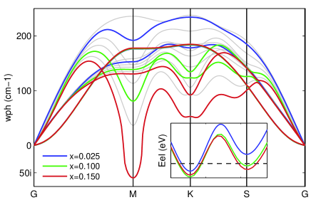
The acoustic parts of the phonon dispersions of are shown for the same electron doping concentrations in Fig. 1. Similar to graphene, pristine has one quadratic and two linear acoustic phonon branches which flatten out around the K and M points in an energy window . Upon doping, the acoustic in-plane branches soften. The parabolic out-of-plane phonons are odd under mirror transformation with respect to the Mo plane and do not couple the conduction band minima at K and . There is thus no Kohn anomaly (or related phenomena) leading to softening of these phonons upon electron doping. At a critical electron concentration one of the acoustic modes develops an instability at the M point, indicating the onset of a CDW regime. At this point the phonon frequency of this mode becomes imaginary (Fig. 1) PhysRevLett.106.196406 . This behavior is reminiscent of , where a CDW-SC transition can be tuned by pressure or Cu intercalation PhysRevLett.103.236401 . However, the CDW regime in already occurs in its pristine state, and is suppressed by pressure or hole-doping, giving way to SC, whereas the sequence of phases we observe in is reversed.
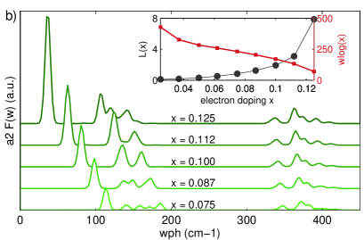
Let us now turn our focus toward the SC regime at intermediate concentrations. We examine the lattice dynamics encoded in the phonon density of states and the Eliashberg function. The phonon density of states (see Suppl. Mat.) has a rich peak structure, with the largest contributions stemming from the regions where the phonon dispersion flattens, leading to characteristic van Hove enhancements. The SC response encoded in the Eliashberg function is dominated by the flat regions (around the M and K points) of the acoustic phonon branches. These features are inherited by the Eliashberg function (Fig. 2), which includes weighting by the electron-phonon coupling matrix elements.
As the acoustic phonon mode with minimum at the M point softens, the evolution of the Eliashberg function displays a maximum integrated intensity at . However, this concentration does not correspond to maximum of since the interplay of the effective coupling and has to be considered. As it can be seen in the inset of Fig. 2 decreases while increases with increasing doping. An optimal proportion is reached at leading to a maximum of . Thus, the combined evolution of and is one reason for the dome-shaped dependence of the SC transition temperature on the electron doping concentration, which can be seen in Fig. 3. Here we show experimental data of Ref. Ye30112012 along with results of our numerical simulation for different Coulomb pseudopotentials . Besides the coincidence in the position of the maximum in at ( cm-2), we also note that the computed and experimental SC transition temperatures are of the same order of magnitude. This is remarkable, since Eliashberg theory is a rather crude approximation, which does not account for pair-breaking effects, such as impurities, incorporates Coulomb interactions only statically as and neglects enhanced phase fluctuations in 2D. It is therefore expected to overestimate . But, this overestimation can be reduced by involving a doping-dependent , which is reasonable, since the Coulomb interaction will clearly change upon electron doping. And indeed, we find an even better quantitative agreement with the experimental data, by adjusting in dependence of the doping concentration, as it can be seen Fig. 3. Hence, we find a second reason for the dome-shape of the .
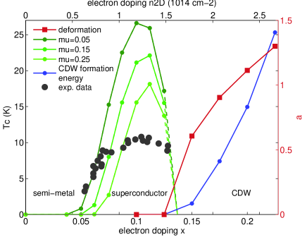

In order to better understand the nature of the SC-CDW phase transition, we examine the doping dependence of the CDW-induced lattice distortion , shown as a red line in Fig. 3. Here, is defined as the angle between three neighboring Mo atoms subtracted by . For an undistorted honeycomb lattice one finds . By relaxing the atomic structure of a 21 supercell, we observe beyond a critical electron concentration of , as forces arise from the unstable phonon mode at lattice vector ge2014 . These distortion effects, depicted in Fig. 4 (a), become more pronounced with increasing electron doping. We note that in addition to the CDW formation, there is a further homogeneous outward relaxation of the S atoms upon electron doping.
The effects of homogeneous S relaxation and CDW formation on the electronic structure are illustrated in Fig. 4 (b) for electron doping 333For these calculations the PAW method in the LDA as implemented in VASP has been used.. In the supercell Brillouin zone, the former band minima at K and are folded almost on top of each other at the supercell K point. In the absence of a CDW, low-energy states originating from K and can be distinguished by their orbital band character. The latter states carry a significant -weight, whereas the conduction band minimum at K has no such admixture (see Fig. 4 (b) left panel). The outward relaxation of the S atoms lowers -derived states from in energy (Fig. 4 (b) middle panel). With increasing CDW amplitude the two bands originating from K and mix, and this hybridization adds to the splitting of the two bands, c.f. Fig. 4 (b) (right panel). This splitting leads to lowering of the electronic energy if the Fermi level lies sufficiently high in the conduction band. The total energy gain upon CDW formation as function of doping level is shown in Fig. 3 (blue line). It illustrates that the CDW formation energies for are comparable to typical Cooper pair condensation energies K ( meV) encountered here, and an interesting competition of the two should emerge.
While the Eliashberg theory of SC order is only applicable as long as the lattice remains stable, it is clear that the competition of CDW and SC order will in any case depend on changes of the Fermi surface due to CDW formation. For the perfect crystal (relaxed structure at zero doping) and a doping level of , two bands would intersect the Fermi level near the supercell K point, and there would be thus two Fermi lines around K. Upon outward relaxation of the S atoms (preserving all lattice symmetries) and formation of the CDW, we observe a Lifschitz transition where one of the Fermi pockets disappears, Fig. 4 (b) (middle and right panel). The system thus remains metallic in the CDW phase, but the SC transition temperatures should be reduced due to the vanishing phase space for inter-pocket scattering. Persisting metallicity in the CDW phase of MoS2 is indeed ensured by the “topology” of the inter-mixing bands at K and , Fig. 4 (c). In TiSe2, CDW bands with opposite slope are folded on top of each other, and a gap can open upon hybridization. However, in MoS2, the slopes of the backfolded bands have the same sign, and avoided crossings do not lead to a full gap, but only reduce the number of Fermi sheets by one.
Since it is known, that the energies of the minima in the counduction band of MoS2 are very sensitive to external strain acs_nanolett the before mentioned change in the Fermi surface topology due to the CDW transition might be sensitive to strain as well. To analyse this behavior we redid the relaxation calculations in the doping range of the inset of the charge density wave for different lattice constants (see Suppl. Mat.). Thereby we found a strong dependence of the critical doping concentration at which the CDW phase sets in to the lattice constant. A strain of less the changes the critical doping concentration by more than . Thus, the competition between the CDW and the SC phase can be triggered and tuned drastically by both, the doping concentration and the external strain.
Conclusions: Electron doped dichalcogenides feature CDW and SC instabilities, driven by the softening of an acoustical phonon mode upon charge doping. Due to the band topology, the M point CDW cannot fully gap the Fermi surface of electron doped MoS2. Therefore, CDW and SC phases may coexist, albeit with reduced SC transition temperatures. In any case, the SC and CDW instabilities rely on the energy differences between the conduction band minima at K and . These are highly sensitive to lattice relaxation, and we speculate that adsorption of molecular species on MoS2 may be useful for tuning superconducting transition temperatures.
The competition of CDW and SC phases is common in metallic transition metal dichalcogenides, such as TiSe2, NbSe2 and TaS2. All these materials differ, however, from MoS2 in that the transition metal atoms lack one (Nb, Ta) or two (Ti) valence electrons in comparison to Mo. Nevertheless, electron doped MoS2 develops CDW/SC instabilities as well, although entirely different bands are involved. The most prominent resulting difference compared to materials like TiSe2 is the reversed order in the phase diagram of MoS2.
Acknowledgments: We are grateful for useful discussions with A.V. Balatsky, I. Gierz, A. Liu, F. Mauri, and M. Calandra. S.H. would like to the thank the Humboldt Foundation for support. This work was supported by the European Graphene Flagship and by the Department of Energy under Grant No. DE-FG02-05ER46240. The numerical computations were carried out on the University of Southern California high performance supercomputer cluster and the Norddeutscher Verbund zur Förderung des Hoch- und Höchstleistungsrechnens (HLRN) cluster.
References
- (1) K. S. Novoselov, D. Jiang, F. Schedin, T. J. Booth, V. V. Khotkevich, S. V. Morozov, and A. K. Geim, Proc. Natl. Acad. Sci. USA 102, 10451 (2005)
- (2) K. C. Rahnejat, C. A. Howard, N. E. Shuttleworth, S. R. Schofield, K. Iwaya, C. F. Hirjibehedin, C. Renner, G. Aeppli, and M. Ellerby, Nature Communications 2, 558 (nov 2011)
- (3) Q. H. Wang, K. Kalantar-Zadeh, A. Kis, J. N. Coleman, and M. S. Strano, Nature Nanotechnology 7, 699 (2012), ISSN 1748-3387
- (4) A. H. Castro Neto, Phys. Rev. Lett. 86, 4382 (May 2001)
- (5) J. van Wezel, P. Nahai-Williamson, and S. S. Saxena, Phys. Rev. B 83, 024502 (Jan 2011)
- (6) F. J. Di Salvo, D. E. Moncton, and J. V. Waszczak, Phys. Rev. B 14, 4321 (Nov 1976)
- (7) E. Morosan, H. Zandbergen, B. Dennis, J. Bos, Y. Onose, T. Klimczuk, A. Ramirez, N. Ong, and R. Cava, Nat Phys 2, 544 (2006)
- (8) A. F. Kusmartseva, B. Sipos, H. Berger, L. Forró, and E. Tutiš, Phys. Rev. Lett. 103, 236401 (Nov 2009)
- (9) M. Calandra and F. Mauri, Phys. Rev. Lett. 106, 196406 (May 2011)
- (10) J. T. Ye, Y. J. Zhang, R. Akashi, M. S. Bahramy, R. Arita, and Y. Iwasa, Science 338, 1193 (2012)
- (11) K. Taniguchi, A. Matsumoto, H. Shimotani, and H. Takagi, Applied Physics Letters 101, 042603 (2012)
- (12) Y. Ge and A. Y. Liu, Phys. Rev. B 87, 241408 (Jun 2013)
- (13) R. B. Somoano, V. Hadek, A. Rembaum, S. Samson, and J. A. Woollam, The Journal of Chemical Physics 62, 1068 (1975)
- (14) G. Kresse and J. Furthmüller, Comput. Mat. Sci., 15(1996)
- (15) G. Kresse and J. Furthmüller, Phys. Rev. B, 11169(1996)
- (16) P. Giannozzi, S. Baroni, N. Bonini, M. Calandra, R. Car, C. Cavazzoni, D. Ceresoli, G. L. Chiarotti, M. Cococcioni, I. Dabo, A. Dal Corso, S. de Gironcoli, S. Fabris, G. Fratesi, R. Gebauer, U. Gerstmann, C. Gougoussis, A. Kokalj, M. Lazzeri, L. Martin-Samos, N. Marzari, F. Mauri, R. Mazzarello, S. Paolini, A. Pasquarello, L. Paulatto, C. Sbraccia, S. Scandolo, G. Sclauzero, A. P. Seitsonen, A. Smogunov, P. Umari, and R. M. Wentzcovitch, Journal of Physics: Condensed Matter 21, 395502 (2009)
- (17) P. B. Allen and R. C. Dynes, Phys. Rev. B 12, 905 (Aug 1975)
- (18) G. M. Eliashberg, Zh. Eksp. Teor. Fiz., 966(1960)
- (19) A. Kuc, N. Zibouche, and T. Heine, Phys. Rev. B 83, 245213 (Jun 2011)
- (20) Y. Ge, W. Wan, W. Feng, D. Xiao, and Y. Yao arXiv:1403.0695
- (21) A. Steinhoff, M. Rösner, F. Jahnke, T. O. Wehling, and C. Gies, Nano Letters 14, 3743 (2014), http://pubs.acs.org/doi/pdf/10.1021/nl500595u, http://pubs.acs.org/doi/abs/10.1021/nl500595u