Cold molecular ions on a chip
Abstract
We report the sympathetic cooling and Coulomb crystallization of molecular ions above the surface of an ion-trap chip. N and CaH+ ions were confined in a surface-electrode radiofrequency ion trap and cooled by the interaction with laser-cooled Ca+ ions to secular translational temperatures in the millikelvin range. The configuration of trapping potentials generated by the surface electrodes enabled the formation of planar bicomponent Coulomb crystals and the spatial separation of the molecular from the atomic ions on the chip. The structural and thermal properties of the Coulomb crystals were characterized using molecular dynamics simulations. The present study extends chip-based trapping techniques to Coulomb-crystallized molecular ions with potential applications in mass spectrometry, cold chemistry, quantum information science and spectroscopy.
pacs:
37.10.Pq, 37.10.Ty, 37.10.MnThe recent development of miniaturized trapping devices providing tightly confining, highly flexible trapping potentials has paved the way for new schemes for the precise control of neutral atoms and atomic ions. The ability to trap and cool neutral atoms on the surface of microstructured chips has enabled new experiments in the realms of, e. g., quantum optics, quantum interferometry and metrology (Reichel and Vuletić, 2011; Fortágh and Zimmermann, 2005; Riedel et al., 2010). Similarly, the development of radiofrequency (RF) ion-trap chips Chiaverini et al. (2005); Stick et al. (2006); Hughes et al. (2011) has laid the basis for improved protocols for the manipulation, addressing and shuttling of ions which is of importance for, e.g., quantum information processing (Kielpinski et al., 2002; Ospelkaus et al., 2011) and quantum simulation (Clark et al., 2011; Szymanski et al., 2012; Buluta et al., 2008).
While chip techniques for atomic species are by now well established, their extension to molecules has proven challenging. Translationally cold molecules and molecular ions are currently of great interest for applications in precision spectroscopy Loh et al. (2013); Hudson et al. (2011), cold chemistry and collision studies (Willitsch et al., 2008; Ospelkaus et al., 2010; Hall and Willitsch, 2012; Kirste et al., 2012), quantum optics (Schuster et al., 2011) and quantum information science (DeMille, 2002; Mur-Petit et al., 2012). However, significant difficulties arise because the complex molecular energy level structure precludes the implementation of closed optical transitions in most cases. Therefore, standard techniques of atomic physics like laser cooling and fluorescence detection of single particles are at best only applicable to a very restricted number of molecular systems (Shuman et al., 2010). For polar neutral molecules such as CO and Rydberg atoms, the deceleration and trapping on a chip has only recently been achieved using their interaction with time-varying inhomogeneous electric fields generated by microstructured electrodes on a surface (Meek et al., 2009; Marx et al., 2013; Hogan et al., 2012).
Here, we report the generation of Coulomb crystals, i.e., ordered structures of translationally cold and spatially localized molecular ions, above the surface of an ion-trap chip. The molecular ions were cooled sympathetically by the interaction with simultaneously trapped laser-cooled atomic ions (Mølhave and Drewsen, 2000; Willitsch, 2012). The trapping potential configuration generated by our chip enabled the formation of two- and three-dimensional atomic-molecular bicomponent Coulomb crystals as well as the spatial separation of both species in layers parallel to the chip surface. Our results illustrate the capabilities of chip-based trapping devices for experiments with cold molecular ions with potential applications in mass spectrometry, cold chemistry, quantum information science and spectroscopy.
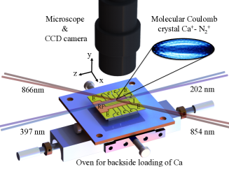
Inspired by Ref. (Allcock et al., 2010), we adopted a 6-wire surface-electrode (SE) ion trap consisting of a split central electrode, two RF electrodes and two batteries of control and endcap electrodes, see Fig. 1. The RF electrodes were used to generate time-varying electric fields for the dynamic trapping of the ions in the transverse ) directions Willitsch (2012). All other electrodes were used to apply static (DC) voltages. The static potentials served to confine the ions in the longitudinal direction, to tilt the principal axes of the trap for efficient laser cooling of the atomic ions Allcock et al. (2010), to compensate excess micromotion Berkeland et al. (1998) and to shape the trapping potentials in order to manipulate the structure of the Coulomb crystals (Szymanski et al., 2012). The width of the RF and central electrodes amounted to 2.00 mm and 750 m, respectively. The width of the gaps between the electrodes was 300 m. The trap electrodes were laser cut out of a 0.50-mm stainless steel foil, electro-polished and coated with a layer of gold with a nominal thickness of 2 m. The trap was glued on a ceramic frame separating the electrodes from a printed circuit board containing the trap electronics. This specific trap layout was chosen in order to avoid any dielectric surfaces in the vicinity of the trap center which could cause the buildup of stray charges and patch potentials.
To load the trap with atomic ions, an atomic beam of neutral calcium was produced by evaporation from a resistively heated stainless steel tube placed underneath the central trap region. The beam passed through a 300 m wide slit operating as a skimmer, the ceramic base of the trap and finally the central gap of the chip (between the two central electrodes) to reach the trap center where Ca+ ions were produced by non-resonant photoionization, see Fig. 1. This backside loading technique has the advantage of avoiding the coating of the chip surface with Ca deposited from the beam (Amini et al., 2010). Doppler laser cooling of Ca+ ions was achieved using three diode laser beams at 397, 866 and 854 nm pumping on the , and transitions.
For the present sympathetic cooling experiments, we chose N (mass 28 amu) and CaH+ (mass 41 amu) as prototypical molecular ions which have a lighter and a heavier mass compared to the laser-cooled Ca+ ions (mass 40 amu), respectively. The N ions were produced above the surface of the chip by resonance-enhanced -photoionization (REMPI) via the intermediate electronic state of neutral N2 Tong et al. (2010) introduced into the vacuum chamber through a leak valve at partial pressure of mbar. REMPI was carried out using the frequency-tripled output of a Nd:YAG-pumped pulsed dye laser operating at a wavelength of 202 nm and a pulse energy of 80. CaH+ ions were produced by chemical reactions of trapped laser-excited Ca+ ions with H2 molecules leaked into the vacuum chamber. All lasers propagated parallel to the chip surface and were superimposed at the trap center. The fluorescence of the Ca+ ions was spatially resolved by a microscope (magnification 11.5) and imaged onto a CCD camera.
The operation of the trap can be understood in terms of an adiabatic approximation for the trapping potentials which assumes that the motion of the ions is slow on the time scale of the RF period (Gerlich, 1992). Within this approximation, the total effective trapping potential experienced by the ions is given by the sum of a time-independent pseudopotential and a static potential generated by the trap electrodes:
| (1) |
Here, and are the charge and mass of the trapped ions, respectively, and and denote the RF amplitude and frequency, respectively. The potential terms and are the solution of the Laplace equation for a unit voltage applied to the RF and the ith DC electrode, respectively. Vi is the voltage applied on the ith DC electrode.
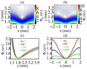
The trapping potentials were calculated by solving the Laplace equation numerically using finite element methods (FEM) as well as using analytical representations of the electrode potentials (Schmied, 2010, 2013). Results of the FEM calculations are presented in Fig. 2. The height of trapping, defined as the position of the pseudopotential minimum where the RF field vanishes (the RF null line), was calculated to be 1.82 mm above the surface. The depth of the pseudopotential , defined as the potential difference between the minimum and the saddle point above the surface through which ions can escape (see Fig. 2 (a)), was calculated to be 117 meV for Ca+ ions at the radiofrequency voltage VRF=495 V and the RF frequency = MHz used in the experiments.
To determine the optimal static voltages applied to the different DC electrodes, the parametrization method of Ref. (Allcock et al., 2010) was used. Typical voltages used in the experiments were central (1,2), control (c), endcap (E) electrodes=2 to 2.3, -6 to -6.6, 21.5 to 23 V. This voltage configuration optimized the total trap depth whilst maintaining the position of the ions at the RF null line to minimize excess micromotion. The application of the static potentials gave rise to saddle points of off-center along the axis providing additional escape routes of the ions from the trap (see Fig. 2 (b)). For Ca+, the effective trap depth was limited by the escape of the ions through these saddle points and was calculated to be 113 meV.
Using the same trapping parameters, the total trapping potential has also been calculated for N, CaH+ and CaO+ ions. From Eq. (1), it can be seen that the pseudopotential is inversely proportional to the ion mass leading to a segregation of the ion species in the Coulomb crystals according to their mass. This situation is completely analogous to the one found in conventional linear RF traps (Willitsch, 2012). Fig. 2 (c) and (d) show one-dimensional cuts of at the trap center along the and -axes for N, CaH+ and CaO+ ions in comparison with Ca+. For the N and CaH+ ions used in the experiments, the effective trap depths were calculated to be 261 meV and 104 meV, respectively.
To characterize the thermal and structural properties of the Coulomb crystals observed in the experiments, we performed molecular dynamics (MD) simulations Bell et al. (2009); Willitsch (2012). Briefly, the classical equations of motion for the laser- and sympathetically cooled ions in the trapping potential were solved numerically. The total force acting on the ions was expressed by
| (2) |
where the terms on the right hand side represent the trapping force, the Coulomb force between ions, the laser cooling force, an effective heating force (reflecting collisions with background gas molecules and imperfections of the setup) and the radiation pressure force generated by unidirectional laser cooling. The laser cooling and radiation pressure forces act only on the atomic ions, while the trapping, Coulomb and heating forces act on both atomic and molecular ions. The ion trajectories obtained from the simulations were used for the reconstruction of the experimental images. A careful comparison of the simulated and experimental images served to determine the number of the ions in the crystal as well as their kinetic energies (Bell et al., 2009). To calculate the trapping forces generated by the chip, three-dimensional Taylor expansions were fitted to the numerical electrode potentials. The trap force in Eq. (2) was calculated from analytical gradients of the fitted potential functions. In the simulations, fully time-dependent potentials were used so that effects related the ion micromotion could be characterized.
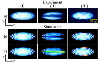
Fig. 3 shows (a) experimental and (b, c) simulated images of typical Coulomb crystals imaged in the plane parallel to the surface of the chip. The molecular ions do not fluoresce and are only indirectly visible as dark areas appearing in the fluorescence images of the crystals. In Fig. 3 (c), the sympathetically cooled molecular ions have been made visible in the simulated images for clarity. Column (I) in Fig. 3 shows a pure atomic Coulomb crystal containing 262 Ca+ ions at a mean secular energy E=23 mK. The secular energy is defined as the thermal energy of the ions without the micromotion. Although the shapes of the crystals projected onto the imaging plane are reminiscent of those obtained in conventional linear RF traps Willitsch (2012), the Coulomb crystals in the SE trap are not spheroidal owing to the lower symmetry of the trapping potentials (see below and Ref. Szymanski et al. (2012)). This is also reflected by the lack of degeneracy of the trap frequencies in the transverse directions. For the present case, the principal trap frequencies have been determined to be kHz, kHz and kHz.
The Ca+-N bicomponent Coulomb crystal shown in Fig. 3 (II) (a) was obtained by loading N into a Ca+ Coulomb crystal as described above. Based on the MD simulations, we inferred that this crystal contains 50 N ions sympathetically cooled to E=43 mK in equilibrium with 180 Ca+ at E=33 mK. Since the trapping potential is steeper for lighter ions (see Fig. 2 (c, d)), the N ions localized closer to the central trap axis than the Ca+ ions. The asymmetric shape of the N crystal along the -direction was caused by the unidirectional radiation pressure force acting on the Ca+ ions as well as small asymmetries in the potential induced by the geometry of the RF electrodes.
Column (III) of Fig. 3 shows 7 CaH+ ions at E=28 mK sympathetically cooled by 200 Ca+ ions at E=24 mK. The heavy CaH+ ions localize at the edges of the Ca+ crystal. We found it difficult to sympathetically cool a larger number of CaH+ ions which we attribute to their reduced contact volume with the laser-cooled Ca+ ions at the extremities of the crystal as well as the reduced trap depth for heavier species.
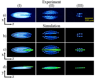
The flexibility in shaping the trapping potentials on the chip lends itself to a precise manipulation of the crystals to form structures which are challenging to obtain in conventional electrode geometries. In the experiment shown in column (I) of Fig. 4, the molecular and atomic ions were pushed away from the RF null line by decreasing the voltages applied to the central electrodes. Because of the mass dependence of the pseudopotential, the two ion species were spatially separated in the direction perpendicular to the surface such that the N ions were located closer to the central trap axis and the Ca+ ions further away. The result were two layers of ions with a mean distance of 192 m according to the MD simulations as can be seen in the side view of the simulated crystal in Fig. 4 (I) (d).
In the experiment shown in column (II) of Fig. 4, a near-planar bicomponent Coulomb crystal was formed with sympathetically cooled N ions centered along the RF null line splitting the Ca+ crystal in two halves. From the simulated side view of the crystal shown in Fig. 4 (II) (d), it can be seen that the crystal has a pancake-like shape and is at maximum only two layers of ions thick.
In the experiment shown in column (III) of Fig. 4, a completely planar structure was generated consisting of a string of 5 N ions sympathetically cooled by two adjacent strings of 3 laser-cooled Ca+ ions each. Such planar bicomponent structures have recently been proposed as a framework for quantum computation and simulation (Buluta and Hasegawa, 2008).
In summary, we have reported the trapping and sympathetic cooling of molecular ions above the surface of an ion-trap chip. The trapping potentials generated by the electrodes on the chip enabled the formation of two-layer and planar bicomponent Coulomb crystals. Capitalizing on the mass dependence of the pseudopotential, spatially separated layers of atomic and molecular ions could be formed. The flexibility and variability in designing electrode structures in SE traps (Schmied et al., 2009; Hughes et al., 2011) pave the way for more sophisticated trapping architectures for cold molecular ions with prospects for separating and individually shuttling the different ion species on the chip. Following the recent development of chip-trap devices for atomic ions Amini et al. (2010); Hughes et al. (2011), highly integrated, multifunctional trapping arrays on a single chip can be envisaged which contain dedicated zones for, e.g., the preparation, cooling, spectroscopy, chemistry and mass spectrometry of molecular ions. These developments offer prospects for a significant simplification of the technological overhead for experiments with molecular ions, which have thus far mainly relied on complex and costly guided-ion beam machines Gerlich (1992).
We gratefully acknowledge the technical support by Dieter Wild and Andreas Tonin. This work was supported by the University of Basel, the COST Action MP1001 ”Ion Traps for Tomorrow’s Applications” and the Swiss National Science Foundation through the National Centre of Competence in Research ”Quantum Science and Technology”.
References
- Reichel and Vuletić (2011) J. Reichel and V. Vuletić, eds., Atom chips (WILEY-VCH, Weinheim, Germany, 2011).
- Fortágh and Zimmermann (2005) J. Fortágh and C. Zimmermann, Science 307, 860 (2005).
- Riedel et al. (2010) M. F. Riedel, P. Böhi, Y. Li, T. W. Hänsch, A. Sinatra, and P. Treutlein, Nature 464, 1170 (2010).
- Chiaverini et al. (2005) J. Chiaverini, R. B. Blakestad, J. Britton, J. D. Jost, C. Langer, D. Leibfried, R. Ozeri, and D. J. Wineland, Quant. Inform. Comp. 5, 419 (2005).
- Stick et al. (2006) D. Stick, W. K. Hensinger, S. Olmschenk, M. J. Madsen, K. Schwab, and C. Monroe, Nat. Phys. 2, 36 (2006).
- Hughes et al. (2011) M. D. Hughes, B. Lekitsch, J. A. Broersma, and W. K. Hensinger, Contemp. Phys. 52, 505 (2011).
- Kielpinski et al. (2002) D. Kielpinski, C. Monroe, and D. J. Wineland, Nature (London) 417, 709 (2002).
- Ospelkaus et al. (2011) C. Ospelkaus, U. Warring, Y. Colombe, K. R. Brown, J. M. Amini, D. Leibfried, and D. J. Wineland, Nature 476, 181 (2011).
- Clark et al. (2011) R. J. Clark, Z. Lin, K. S. Diab, and I. L. Chuang, J. Appl. Phys. 109, 076103 (2011).
- Szymanski et al. (2012) B. Szymanski, R. Dubessy, B. Dubost, S. Guibal, J. P. Likforman, and L. Guidoni, Appl. Phys. Lett. 100, 171110 (2012).
- Buluta et al. (2008) I. M. Buluta, M. Kitaoka, S. Georgescu, and S. Hasegawa, Phys. Rev. A 77, 062320 (2008).
- Loh et al. (2013) H. Loh, K. C. Cossel, M. C. Grau, K.-K. Ni, E. R. Meyer, J. L. Bohn, J. Ye, and E. A. Cornell, Science 342, 1220 (2013).
- Hudson et al. (2011) J. J. Hudson, D. M. Kara, I. J. Sallman, B. E. Sauer, M. R. Tarbutt, and E. A. Hinds, Nature 473, 493 (2011).
- Willitsch et al. (2008) S. Willitsch, M. T. Bell, A. D. Gingell, S. R. Procter, and T. P. Softley, Phys. Rev. Lett. 100, 043203 (2008).
- Ospelkaus et al. (2010) S. Ospelkaus, K.-K. Ni, D. Wang, M. H. G. de Miranda, B. Neyenhuis, G. Quéméner, P. S. Julienne, J. L. Bohn, D. S. Jin, and J. Ye, Science 327, 853 (2010).
- Hall and Willitsch (2012) F. H. J. Hall and S. Willitsch, Phys. Rev. Lett. 109, 233202 (2012).
- Kirste et al. (2012) M. Kirste, X. Wang, H. C. Schewe, G. Meijer, K. Liu, A. van der Avoird, L. M. C. Janssen, K. B. Gubbels, G. C. Groenenboom, and S. Y. T. van de Meerakker, Science 338, 1060 (2012).
- Schuster et al. (2011) D. I. Schuster, L. S. Bishop, I. L. Chuang, D. DeMille, and R. J. Schoelkopf, Phys. Rev. A 83, 012311 (2011).
- DeMille (2002) D. DeMille, Phys. Rev. Lett. 88, 067901 (2002).
- Mur-Petit et al. (2012) J. Mur-Petit, J. J. García-Ripoll, J. Pérez-Ríos, J. Campos-Martínez, M. I. Hernández, and S. Willitsch, Phys. Rev. A 85, 022308 (2012).
- Shuman et al. (2010) E. S. Shuman, J. F. Barry, and D. DeMille, Nature 467, 820 (2010).
- Meek et al. (2009) S. A. Meek, H. Conrad, and G. Meijer, Science 324, 1699 (2009).
- Marx et al. (2013) S. Marx, D. Adu Smith, M. J. Abel, T. Zehentbauer, G. Meijer, and G. Santambrogio, Phys. Rev. Lett. 111, 243007 (2013).
- Hogan et al. (2012) S. D. Hogan, P. Allmendinger, H. Saßmannshausen, H. Schmutz, and F. Merkt, Phys. Rev. Lett. 108, 063008 (2012).
- Mølhave and Drewsen (2000) K. Mølhave and M. Drewsen, Phys. Rev. A 62, 011401 (2000).
- Willitsch (2012) S. Willitsch, Int. Rev. Phys. Chem. 31, 175 (2012).
- Allcock et al. (2010) D. T. C. Allcock, J. A. Sherman, D. N. Stacey, A. H. Burrell, M. J. Curtis, G. Imreh, N. M. Linke, D. J. Szwer, S. C. Webster, A. M. Steane, and D. M. Lucas, New J. Phys. 12, 053026 (2010).
- Berkeland et al. (1998) D. J. Berkeland, J. D. Miller, J. C. Bergquist, W. M. Itano, and D. J. Wineland, J. Appl. Phys. 83, 5025 (1998).
- Amini et al. (2010) J. M. Amini, H. Uys, J. H. Wesenberg, S. Seidelin, J. Britton, J. J. Bollinger, D. Leibfried, C. Ospelkaus, A. P. VanDevender, and D. J. Wineland, New J. Phys. 12, 033031 (2010).
- Tong et al. (2010) X. Tong, A. H. Winney, and S. Willitsch, Phys. Rev. Lett. 105, 143001 (2010).
- Gerlich (1992) D. Gerlich, in Advances in Chemical Physics Series, Vol. 82, edited by C.-Y. Ng and M. Baer (John Wiley & Sons Inc., 1992) p. 1.
- Schmied (2010) R. Schmied, New J. Phys. 12, 023038 (2010).
- Schmied (2013) R. Schmied, “SurfacePattern software package,” (2013).
- Bell et al. (2009) M. T. Bell, A. D. Gingell, J. Oldham, T. P. Softley, and S. Willitsch, Faraday Discuss. Chem. Soc. 142, 73 (2009).
- Buluta and Hasegawa (2008) I. M. Buluta and S. Hasegawa, Phys. Rev. A 78, 042340 (2008).
- Schmied et al. (2009) R. Schmied, J. H. Wesenberg, and D. Leibfried, Phys. Rev. Lett. 102, 233002 (2009).