Plasmons and screening in monolayer and multilayer black phosphorus
Abstract
Black phosphorus exhibits a high degree of band anisotropy. However, we found that its in-plane static screening remains relatively isotropic for momenta relevant to elastic long-range scattering processes. On the other hand, the collective electronic excitations in the system exhibit a strong anisotropy. Band non-parabolicity leads to a plasmon frequency which scales as , where is the carrier concentration, and . Screening and charge distribution in the out-of-plane direction are also studied using a non-linear Thomas-Fermi model.
Introduction— Black phosphorus (BP) is one of the thermodynamically more stable phases of phosphorus, at ambient temperature and pressure. It is a layered material, with each layer forming a puckered surface due to hybridization. In its bulk crystalline form Keyes (1953); Warschauer (1963); Jamieson (1963); Morita (1986); Chang and Cohen (1986), BP is a semiconductor with a direct band gap of about eV with measured Hall mobilities in and type samples approaching cm2/Vs. Recent rediscovery of BP Reich (2014); Li et al. (2014); Liu et al. (2014); Xia et al. (2014); Koenig et al. (2014); Castellanos-Gomez et al. (2014) in its multilayer form revealed highly anisotropic electrical and optical properties.
In this paper we examine the collective electronic excitations of BP, and its electrostatic screening behavior both along the in- and out-of-plane directions. We calculate the dielectric function , at finite frequency and wavevector q, for monolayer and multilayers of BP within the Random Phase Approximation (RPA), using an effective low-energy Hamiltonian Rodin et al. (2014). The inherent anisotropy of screnning is studied, and the out-of-plane screening properties of multi-layer BP flakes are considered within a non-linear Thomas-Fermi model. The 2D plasmon modes, which are obtained from the zeros of the dielectric function, or the electron loss spectra, , show a highly anisotropic plasmon dispersion, , and we studied its scaling behavior with doping. Lastly, we discuss the implications of our results for basic electrical and light scattering experiments.
Hamiltonian— BP has an orthorhombic crystal structure consisting of puckered layers. The lattice constant in the out-of-plane direction is about Å, and the effective layer-to-layer distance is half of this value Morita (1986). In monolayer BP, translational symmetry in the direction is broken, and its bandstructure has a direct energy gap at the point instead of the Z point in the bulk case. Based on theory and symmetry arguments, the in-plane electron dispersion around the point can be described by the following low-energy Hamiltonian Rodin et al. (2014),
| (3) |
where and are related to the effective masses, while and describe the effective couplings between the conduction and valence bands. and are the energies of the conduction and valence band edges. At present, the energy gap for monolayer BP has not been measured experimentally, but recent ab initio calculation based on the GW method found an energy gap of eV Tran et al. (2014); Rudenko and Katsnelson (2014).
Unlike other layered materials such as graphene and the transition metal dichalcogenides (TMDs), electrons in BP are energetically highly dispersive along the out-of-plane direction. Cyclotron resonance experiments on bulk BP Narita et al. (1983) found an out-of-plane effective mass considerably smaller than that of TMDs Mattheiss (1973). For multilayer BP, confinement in the out-of-plane direction leads to multiple subbands. The in-plane dispersion within each subband can be described by Eq. (3), where are being replaced with . More explicitly, is given by , where labels the subband, is the thickness of the BP film, and is the electron effective mass along . Analogous expressions apply also for the hole case. The quantities are chosen such that it reproduces the energy gap of the BP film Tran et al. (2014), of 2 eV and 0.3 eV in the monolayer and bulk limit respectively. In this work, we adopt an average of experimental Narita et al. (1983) and theoretically Narita et al. (1983); Low et al. (2014) predicted quantization mass i.e. and .
The in-plane dispersion is mainly determined by the parameters , and . These parameters are chosen such that they yield the known anisotropic effective masses. In the bulk BP limit, we have , and Morita (1986); Narita et al. (1983), and for monolayer BP Low et al. (2014). Using this knowledge, we arrive at the following parameter set; , , , and eVm. The value of is taken to be eVm2 Low et al. (2014), where Å and is the width of the BZ in direction.

Dielectric function— The dielectric function of an electron gas in the RPA can be written as,
| (4) |
where is the 2D Coulomb interaction and describes the effective dielectric constant of the medium, which for a common substrate, SiO2, is . is the 2D polarizability (i.e. the pair bubble diagram) given by,
| (5) | |||||
where , denote conduction/valence bands, while are the subband indices and is the spin degeneracy. and are the eigen-energies and eigen-functions after diagonalizing . is the Fermi distribution function, where is the chemical potential. Finite damping can be modeled with the phenomenological broadening term . Allowed optical transitions between these quantized subbands occur when (i.e. intra- and inter-band processes) and . Otherwise the matrix element in Eq. (5) vanishes.
Screening— In the static limit, we generalize the well-known analytical form of the polarizability for 2D electron gas (2DEG) Lindhard (1954) to include anisotropy. Since , we deal only with intraband processes. In the and limits, we have Kittel (2004),
| (6) | |||||
where we have made the transformation,
| and | (7) |
where is the mass tensor with diagonal elements and , is the 2D density-of-states mass given by , and . After some algebra, we arrive at
| (8) |
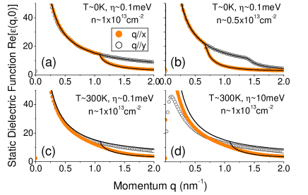
where is the 2D density-of-states. We make an interesting remark: for , we see that reduces to the familiar relation for the static polarization of a 2DEG, . Long range potentials, such as those induced by charged impurities, involve momenta such that , so that screening will be isotropic, at least in the zero temperature and disorder limits.
Fig. 1(a) compares the static dielectric function obtained numerically with the analytical model in Eq. (8), with excellent agreement in the limits of the model. has a kink at . Fig. 1(b) illustrates how the kink migrates with change in doping. With increasing temperature and disorder, the kink is smoothed out as illustrated in Fig. 1(c)-(d), showing obvious deviation from the analytical model. The otherwise isotropic screening at small momenta now becomes anisotropic. On the other hand, dynamical screening, , in BP exhibits strong directional dependence with q. Anisotropic dynamic screening might have important implications to carrier relaxation processes such as scattering with polar optical phonons. In Suppl. Info, we show the calculated real and imaginary part of at finite .

Plasmon dispersion— The zeros of the dynamical dielectric function yield the excitation spectrum of the plasmon modes of the electron gas. The loss function, defined as , quantifies the spectral weight of the plasmon mode, which presents itself as a delta peak in the limit of zero damping. Experimentally, can be quantified with EELS. In the long wavelength limit, i.e. , these modes are well-described by classical Maxwell theory. We consider a BP film sandwiched between two dielectric media and . The bound modes, i.e. plasmons, are characterized by an in-plane wavevector q pointing at an angle with respect to . The dispersion relation for the bound mode can be obtained from the solution to the following equation,
| (9) |
where () is the total admittance, with and , and , . and are the speed of light and admittance of free space, respectively. The matrix elements of are expressed in terms of , the diagonal components of the 2D BP conductivity tensor,
| (10) |
In the limits and , Eq. 9 reduces to
| (11) |
In the non-retarded regime, i.e. , hence , we obtain the ‘quasi-static’ approximation,
| (12) |
where . For frequencies up to the mid-infrared, the conductivity can be approximated by the Drude model,
| , | (13) |
where is the Drude weight and denotes the subbands. Within the model Hamiltonian, the in-plane electron effective masses in vicinity to the point are given by the following expressions Rodin et al. (2014),
| , | (14) |
where is the subband energy gap. Similar expressions apply for the hole case. Note that in graphene, instead. With Eq. (12) and (13), we have the classical plasmon dispersion along the directions, which is .


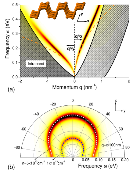
Fig. 2(a) plots the RPA loss function for momentum along the two main crystallographic directions for monolayer BP, with an electron doping of cm-2. The plasmon disperses differently due to their mass anisotropy, where the smaller mass along leads to higher resonance frequency. Classical plasmon dispersion agrees well with the RPA result in the long wavelength limit. Due to the energy gap of eV for monolayer BP, Landau damping occurs preferentially via intraband processes. This occurs when plasmon enters the SP phase space, whose boundaries are given by, . Our calculation suggests that the plasmon along the direction is damped at mid-infrared frequencies, while the plasmon along persists up to the near infrared.
The results reported here can be tested by EELS. In addition, plasmon modes in layered materials Grigorenko et al. (2012); Low and Avouris (2014); Stauber (2014) can also be probed by Fourier transform infrared (FTIR) light scattering experiments of nanostructures Yan et al. (2013); Ju et al. (2011) or with infrared nano-microscopy techniques Fei et al. (2012); Chen et al. (2012). For example, nanostructures exhibit prominent resonances in their extinction spectra due to localized plasmons with odd multiple of the momentum where can be the width of nanoribbons, or the diameter of nano-disks. Fig. 2(b) shows for different angular orientation of q for a momentum corresponding to nanostructures of nm in size. Dashed lines are solutions of Eq. 9. The results suggest polarization sensitive mid-infrared plasmonic resonances in the absorption spectra in BP nanostructures.
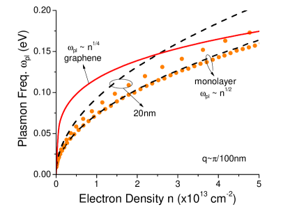
Fig. 3 studies the scaling of plasmon frequency (along ) with carrier concentration . For monolayer BP, we obtain the expected scaling relation of , as in conventional 2DEGs. However, for thicker samples, we found that , with instead. This deviation is due to the strong non-parabolicity caused by interband coupling, particularly when the energy gap of the BP film is . Hence, non-parabolicity effects are more prominent for thicker films. We also note the general trend of increasing Drude weight with film’s thickness due to the decreasing effective masses (see Suppl. Info.).
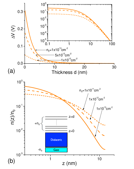
Screening and charge distribution in multilayers— We complete our study by considering the charge distribution and the electrostatic screening in few-layer BP sheets. For this aim we use a non-linear TF theory, which has been shown to properly account for the screening properties of graphite Pietronero et al. (1978); Datta et al. (2008); Kuroda et al. (2011) and MoS2 Castellanos Gomez et al. (2013). We start by considering a given charge transfer between the substrate and the BP flakes, whose origin can be due to charge impurities in the substrate or to the action of a gate voltage. This charge transfer leads to a net surface charge density while a layer below the substrate acquires a charge of , see inset of Fig. 4(b). For a BP sample of thickness , the electrostatic potential and the carrier distribution as a function of the distance from the substrate can be obtained from the energetic balance between kinetic and interlayer capacitance terms, which leads to the non-linear differential equation Castellanos Gomez et al. (2013)
| (15) |
where and we have defined , where nm and are the interlayer separation and dielectric constant, respectively Morita (1986). Using the boundary conditions and , one can obtain the charge density from the solution of the integral equation
| (16) |
On the other hand, the potential difference across a BP sample of thickness can be shown to be given by Castellanos Gomez et al. (2013):
| (17) |
where we have defined the dimensionless parameter .
The potential difference obtained from the above model is shown, for different carrier concentrations, in Fig. 4(a) for a n-doped sample (see Suppl. Info. for results also on p-doped samples). The screening of charged impurities or the gate potential increases as the thickness of the BP layer grows. The dependence of on suggests an intermediate screening behavior between the strong coupling limit of graphene, where the carriers concentrate close to the interface Datta et al. (2008), and the weak coupling regime with reduced screening properties that dominates the screening of MoS2 Castellanos Gomez et al. (2013). Our results suggest that the gate will have negligible effect nm into the bulk of BP, consistent with recent experiments on multilayers BP transistors Xia et al. (2014). We have also calculated for a sample with a given thickness but different charge carrier concentrations as shown in Fig. 4(b). We observe a strong dependence of the screening strength on , such that stronger screening is achieved for larger . Interestingly, from those results one could infer a screening length of the order of the inter-layer spacing for , whereas for lower concentrations, like , the screening length is one order of magnitude larger.
Conclusions— In conclusion, we have studied the screening properties of BP using a combination of RPA for the dynamic and static in-plane screening, as well as for the dispersion of the collective (plasmon) excitations, and a non-linear TF theory for the inter-layer screening. Whereas we find a relatively isotropic static screening, the band non-parabolicity leads to highly anisotropic plasmons. Most saliently, we find that for multilayer samples, the plasmon resonance scales with doping as , where . Furthermore, the modes dispersing along one of the crystallographic directions are long lived, being Landau damped (i.e. decaying into intra-band electron-hole pairs) only for high frequencies, near the infrared. Finally, we find that the charge distribution along the layers and the strength of the electric field screening in BP flakes seem to be between the strong coupling regime characteristic of graphene, and the weak coupling regime of the TMD semiconductors, such as MoS2.
Acknowledgements— FG and RR acknowledge support from the Spanish Ministry of Economy (MINECO) through Grant No. FIS2011-23713, the European Research Council Advanced Grant (contract 290846), and the European Commission under the Graphene Flagship, contract CNECT-ICT-604391. R.R. acknowledges financial support from the Juan de la Cierva Program.
References
- Keyes (1953) R. W. Keyes, Physical Review 92, 580 (1953).
- Warschauer (1963) D. Warschauer, Journal of Applied Physics 34, 1853 (1963).
- Jamieson (1963) J. C. Jamieson, Science 139, 1291 (1963).
- Morita (1986) A. Morita, Applied Physics A 39, 227 (1986).
- Chang and Cohen (1986) K. J. Chang and M. L. Cohen, Physical Review B: Condensed Matter 33, 6177 (1986).
- Reich (2014) E. S. Reich, Nature 506, 19 (2014).
- Li et al. (2014) L. Li, Y. Yu, G. J. Ye, Q. Ge, X. Ou, H. Wu, D. Feng, X. H. Chen, and Y. Zhang, Nature Nanotechnology (2014).
- Liu et al. (2014) H. Liu, A. T. Neal, Z. Zhu, D. Tomanek, and P. D. Ye, arXiv:1401.4133 (2014).
- Xia et al. (2014) F. Xia, H. Wang, and Y. Jia, arXiv:1402.0270 (2014).
- Koenig et al. (2014) S. P. Koenig, R. A. Doganov, H. Schmidt, A. H. Neto, and B. Oezyilmaz, Appl. Phys. Lett. 104, 103106 (2014).
- Castellanos-Gomez et al. (2014) A. Castellanos-Gomez, L. Vicarelli, E. Prada, J. O. Island, K. L. Narasimha-Acharya, S. I. Blanter, D. J. Groenendijk, and e. al, arXiv preprint arXiv:1403.0499 (2014).
- Rodin et al. (2014) A. S. Rodin, A. Carvalho, and A. H. Neto, arXiv:1401.1801 (2014).
- Tran et al. (2014) V. Tran, R. Soklaski, Y. Liang, and L. Yang, arXiv:1402.4192 (2014).
- Rudenko and Katsnelson (2014) A. N. Rudenko and M. I. Katsnelson, arXiv:1404.0618 (2014).
- Narita et al. (1983) S.-i. Narita, S.-i. Terada, S. Mori, K. Muro, Y. Akahama, and S. Endo., Journal of the Physical Society of Japan 52, 3544 (1983).
- Mattheiss (1973) L. F. Mattheiss, Physical Review B 8, 3719 (1973).
- Low et al. (2014) T. Low, A. S. Rodin, A. Carvalho, Y. Jiang, H. Wang, F. Xia, and A. H. C. Neto, Submitted (2014).
- Lindhard (1954) J. Lindhard, Kgl. Danske Videnskab. Selskab Mat.-Fys. Medd 28 (1954).
- Kittel (2004) C. Kittel, Introduction to Solid State Physics (Wiley, 2004).
- Grigorenko et al. (2012) A. N. Grigorenko, M. Polini, and K. S. Novoselov., Nature Photonics 6, 749 (2012).
- Low and Avouris (2014) T. Low and P. Avouris, ACS Nano 8, 1086 (2014).
- Stauber (2014) T. Stauber, Journal of Physics: Condensed Matter 26, 123201 (2014).
- Yan et al. (2013) H. Yan, T. Low, W. Zhu, Y. Wu, M. Freitag, X. Li, F. Guinea, P. Avouris, and F. Xia, Nature Photonics 7, 394 (2013).
- Ju et al. (2011) L. Ju, B. Geng, J. Horng, C. Girit, M. Martin, Z. Hao, and H. A. B. e. al., Nature Nanotechnology 6, 630 (2011).
- Fei et al. (2012) Z. Fei, A. S. Rodin, G. O. Andreev, W. Bao, A. S. McLeod, M. Wagner, and L. M. Z. e. al., Nature 487, 82 (2012).
- Chen et al. (2012) J. Chen, M. Badioli, P. Alonso-González, S. Thongrattanasiri, F. Huth, J. Osmond, and M. S. e. al., Nature 487, 77 (2012).
- Pietronero et al. (1978) L. Pietronero, S. Strässler, H. R. Zeller, and M. J. Rice, Physical Review Letters 41, 763 (1978).
- Datta et al. (2008) S. S. Datta, D. R. Strachan, E. J. Mele, and A. C. Johnson, Nano letters 9, 7 (2008).
- Kuroda et al. (2011) M. A. Kuroda, J. Tersoff, and G. J. Martyna, Physical Review Letters 106, 116804 (2011).
- Castellanos Gomez et al. (2013) A. Castellanos Gomez, E. Cappelluti, R. Roldán, N. Agraït, F. Guinea, and G. Rubio-Bollinger, Advanced Materials 25, 899 (2013).